background image

9.1.2. RF test

9.1.2.1. Preparation for RF test

1. Remove the under cabinet (Refer to 6. DISASSEMBLY 

INSTRUCTION 1.)

16

PDF created with pdfFactory Pro trial version 

www.pdffactory.com

Summary of Contents for KX-TDA0142CE

Page 1: ...manufacture of this product the printed circuit boards will be marked PbF Standard leaded Pb solder can be used as usual on boards without the PbF mark When this mark does appear please read and follow the special instructions described in this manual on the use of PbF and how it might be permissible to use Pb solder during service and repair work 1 ABOUT LEAD FREE SOLDER PbF Pb free Note In the i...

Page 2: ...elting point approximately 1100 F 600 C If you must use Pb solder on a PCB manufactured using PbF solder remove as much of the original PbF solder as possible and be sure that any remaining is melted prior to applying the Pb solder When applying PbF solder to double layered boards please check the component side for excess which may flow onto the opposite side See figure below 1 1 SUGGESTED PbF SO...

Page 3: ...When repairing the following precautions will help prevent recurring malfunctions 1 Cover the plastic parts boxes with aluminum foil 2 Ground the soldering irons 3 Use a conductive mat on the worktable 4 Do not touch IC or LSI pins with bare fingers 3 CAUTION 3 1 NOTE When you note the serial number write down all of the 11 digits The serial number may be found on the label affixed to the bottom o...

Page 4: ...ion Scheme GFSK Roll off factor 0 5 50 roll off in the transmitter Data Coding for Modulator Differential Coding Voice CODEC 32 kbps ADPCM CCITT G 721 Operation range Up to 300 m outdoors Up to 50 m indoors Transmission Output Average 10 mW Peak 250 mW Operating conditions 0 40 C 20 80 relative air humidity not condensing Dimension Cell Station 140 L mm 172 W mm 34 D mm 5 1 2 6 25 32 1 Weight abou...

Page 5: ...port 1 Accessory and User supplied ltems for the CS Accessory screw x 2 washer x 2 ferrite core x 1 User supplied RJ11 connector 5 1 Connecting the CS 1 Connect the cable from the CS interface card to the CS 5 PDF created with pdfFactory Pro trial version www pdffactory com ...

Page 6: ...ugh the groove of the CS in any direction depending on your convenience Wrap the cable once around the ferrite core Then close the case of the ferrite core 6 PDF created with pdfFactory Pro trial version www pdffactory com ...

Page 7: ...Note If you need to open the ferrite core use a flathead screwdriver to unlatch the case of the ferrite core 7 PDF created with pdfFactory Pro trial version www pdffactory com ...

Page 8: ...SASSEMBLY INSTRUCTIONS 1 Remove 5 Screws A 2 Remove the Bottom Cabinet 2 Remove the Solder on Cable of the Main Board by the Soldering iron 8 PDF created with pdfFactory Pro trial version www pdffactory com ...

Page 9: ...he Front Cabinet 2 Remove the RF unit from the Main Board 7 TROUBLESHOOTING GUIDES 7 1 Portable Station PS cannot register to cell station CS or PS does not link CS 9 PDF created with pdfFactory Pro trial version www pdffactory com ...

Page 10: ...7 2 RF check flowchart for Cell Station CS 10 PDF created with pdfFactory Pro trial version www pdffactory com ...

Page 11: ...11 PDF created with pdfFactory Pro trial version www pdffactory com ...

Page 12: ...12 PDF created with pdfFactory Pro trial version www pdffactory com ...

Page 13: ...A0142 4 AC Adaptor or Battery Box PSZZTD142CE 8 1 Initial setting 1 1 Connect KX TDA0142CE to your PC with the Service JIG cable and then power on KX TDA0142CE with a Power supply adaptor 1 2 Property Please set property as follows Port COM1 Bit per second 19200 Data bits 8 Parity None Stop bit 1 Flow control Xon Xoff 1 3 ASCII setup 13 PDF created with pdfFactory Pro trial version www pdffactory ...

Page 14: ...software version is appeared on display If version of TDA0142CE is appeared then operation of CPU is OK Note show software version The number of the version are not concerned with the CS login mode performance If version of software is appeared then operation of CPU is OK 8 2 How to check the status of CS with a PC program Initial setting 14 PDF created with pdfFactory Pro trial version www pdffac...

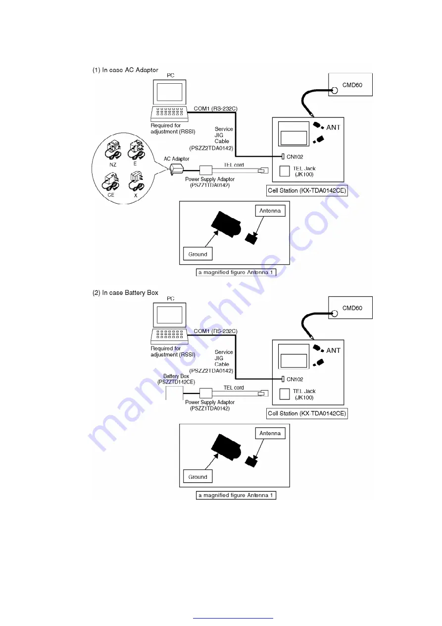
Page 15: ...ansmit the carrier Fault Fault CS is not active 9 TEST AND ADJUSTMENT 9 1 TEST AND ADJUSTMENT FOR RF PART Note About the software version Update the software to the latest version before performing the RF test 9 1 1 Required Equipments 1 CMD60 2 PC Personal Computer with serial port Windows2000 98 or previous version with communication software 3 Power Supply Adaptor PSZZ1TDA0142 4 Service JIG cab...

Page 16: ...9 1 2 RF test 9 1 2 1 Preparation for RF test 1 Remove the under cabinet Refer to 6 DISASSEMBLY INSTRUCTION 1 16 PDF created with pdfFactory Pro trial version www pdffactory com ...

Page 17: ...he CMD60 PMID 0000 TRAFFIC SLOT 0 TRAFFIC CARRIER 5 6 Set Dip switch pin 1 pin 5 and pin 6 from OFF to ON 7 Connect power supply cable and AC adaptor 9 1 2 2 RF test 1 Set the CMD60 to MANUAL TEST 2 Set the CMD60 TRAFFIC CARRIER to 5 3 Press ACCEPT RFPI and SETUP CONNECT on the CMD60 4 Check Power NTP must be 20 to 25dBm 5 Press MODULATION 6 Set Data Type to FIG 31 7 Check the Frequency Offset mus...

Page 18: ...epeated on Traffic Carrier 0 and 9 Make sure to set all dip switches to OFF after RF test 9 1 3 Adjustment RSSI 9 1 3 1 Preparation for adjustment RSSI 1 Remove the under cabinet Refer to 6 DISASSEMBLY INSTRUCTION 1 2 Remove 2 antennas from CN103 and CN104 Refer to 6 DISASSEMBLY INSTRUCTION 2 3 Remove the P C B from upper cabinet Refer to 6 DISASSEMBLY INSTRUCTION 3 4 Solder cable to ANT1 CN103 Re...

Page 19: ...111 RF LEVEL 40 dBm 40 dBm 6 Set Dip switch all pins to OFF 7 Connect the PC to the CS by service JIG cable 8 Start up the PC and start the hyper terminal 9 Set the hyper terminal property as follows also refer to 8 1 initial setting serial port setup Port COM1 Bit per second 19200 Data bits 8 Parity None Stop bit 1 Flow control Xon Xoff 19 PDF created with pdfFactory Pro trial version www pdffact...

Page 20: ...CA1 via power supply adaptor PSZZ1TDA0142 9 1 3 2 Adjustment RSSI test Description of RSSI Calibration Process Text following Command is the input command for the terminal connected to the CS Text following Response is the terminal display response data Confirm the response before proceeding to the next step If no response is set shut off power and repeat from the beginning 20 PDF created with pdf...

Page 21: ...counter 2 PC Personal Computer with serial port Windows 2000 98 or previous version 3 Power supply adaptor PSZZ1TDA0142 4 Service JIG cable PSZZ2TDA0142 5 AC Adaptor KX TCA1 or Battery Box PSZZTD142CE 21 PDF created with pdfFactory Pro trial version www pdffactory com ...

Page 22: ...04 Refer to 6 DISASSEMBLY INSTRUCTIONS 3 Remove the P C B from the upper cabinet Refer to 6 DISASSEMBLY INSTRUCTIONS 4 Connect PC to the CS by service JIG cable 5 Start up the PC and start the hyperterminal 6 Set the hyperterminal property as follows 22 PDF created with pdfFactory Pro trial version www pdffactory com ...

Page 23: ...the TEL jack from the AC adaptor KX TCA1 via power supply Adaptor PSZZ1TDA0142 8 Connect the frequency counter probes the P C B the test pads SYRI GND 9 2 3 Adjustment RF Clock Description of RF Calibration Process Text following Command is the input command for the terminal connected to the CS Text following Response is the terminal display response data Confirm the response before proceeding to ...

Page 24: ...o a value higher than current value XX 4 Repeat 2 to 3 until frequency is within test standard If measured frequency is within the range of 10 386 MHz 20 Hz proceed to next step 5 Send Write command to non volatile memory and write calibration data Command 1216000002040500YY00 Response 0F5601 6 Send CS reset command and reset CS Command 0E0700 Response none 7 Measure frequency RF clock at SYRI aga...

Page 25: ... IC101 is stored in this Flash Memory too When CS starts up the FPGA data is downloaded to the FPGA from the Flash Memory via the CPU Furthermore calibration data for RSSI measurement and clock is stored in the Flash Memory too 1Mbit SRAM is used as the work area CN102 is the communication port for service purpose CN102 is connected to the serial port of the CPU SW100 is 6bits DIP switch to set th...

Page 26: ...en the size of buffered data reaches certain value HDLC IC interrupts to the CPU Then the CPU reads the control data from HDLC IC Voice channel contains 4 ADPCM data And superframe synchronization signal is carried by HK bit of control channel 4 ADPCM data and superframe synchronization signal is transferred to FPGA IC101 Note The GND of CS KX TDA0142 is not common to the GND of the PBX itself car...

Page 27: ... BBIC 4 Address decoder internal registers Address decoder to generate chip select signal for other ICs and internal 16bytes registers to set FPGA operation 5 HDLC IC level shifter The power supply voltage of HDLC IC IC112 is 5V so that HDLC IC cannot be connected to CPU directly because of overvoltage The address bus and data bus of the CPU is connected to HDLC IC via FPGA which has 5V tolerant I...

Page 28: ...hase Locked Loop control The TXDA signal is used to control the modulation of this frequency to 1 87GHz to 1 93GHz Received signals are demodulated filtered and sent to the BBIC via the RXDA line The RSSI Radio Signal Strength Indicator signal enables the implementation of diversity switching whereby two antennas can be mounted in different orientations and their signals compared The one with bett...

Page 29: ...ndary super capacitor 12 7 CLOCK CIRCUIT Three kinds of clock is used in CS CPU CLOCK CPU clock and FPGA clock is used 9 6MHz divided cycle of 19 2MHz TCXO BBIC CLOCK 10 368MHz VCXO is used Tweak frequency by changing the variable capacitance diode by DA signal from CPU DNIC CLOCK 10 24MHz crystal oscillator is used It is used for Reference Clock of DNIC 12 8 RESET CIRCUIT It is reset by the signa...

Page 30: ... TXON O 11 A2 I Active Active 61 VSS VSS 12 A1 I Active Active 62 VDD VDD 13 A0 I Active Active 63 no use ANT3 O 14 VDD VDD 64 no use CP O 15 VSS VSS 65 SYEN O Active Normal 16 INT1 O Normal Active 66 no use SYLD I 17 INT2 O Normal Active 67 SYCL O Active Active 18 RDQ I Normal Active 68 SYDA O Active Active 19 WRQ I Normal Active 69 ANT2 O Active Normal 20 ALE I Normal Active 70 ANT1 O Active Nor...

Page 31: ... O 36 no use A02 O 86 no use ADPIN I 37 no use AFR2 O 87 IOMCLK I Fixed 38 no use ACL O 88 no use MPCLK O 39 no use AIN1 I 89 no use CLK10 O 40 no use A01 O 90 VDD5 VDD5 41 no use AFR1 O 91 VDD VDD 42 VSS VSS 92 VSS VSS 43 VDD VDD 93 AD7 I O Active Active 44 no use PCMIN I 94 AD6 I O Active Active 45 no use PCMOUT O 95 AD5 I O Active Active 46 no use PCMCL O 96 AD4 I O Active Active 47 no use PCMF...

Page 32: ... GND GND 73 GND GND 18 PCMCL I 74 no use TXA 19 A3 I Active Active 75 HK_DET_O O 20 A2 I Active Active 76 no use TXB 21 A1 I Active Active 77 no use PA3 O 22 A0 I Active Active 78 no use PA2 O 23 A5 I Active Active 79 no use PA1 O 24 VCCINT VCC 80 no use PA0 O 25 GND GND 81 GND GND 26 A4 I Active Active 82 VCCINT VCC 27 D7 I O Active Active 83 ECLK O Active 28 D6 I O Active Active 84 C2M_I I Activ...

Page 33: ...44 no use PCMIN I 100 A2 for HDLC O Active 45 GND GND 101 A1 for HDLC O Active 46 no use PCMOUT O 102 A0 for HDLC O Active 47 no use PCMFS3 I 103 D7 for HDLC I O Active 48 no use PCMFS2 I 104 NC 49 no use PCMFS1 I 105 NC 50 no use PCMFS0 I 106 M2 I 51 GWAIT O Normal Active 107 VCC0 VCC 52 GND GND 108 VCC0 VCC 53 VCC0 VCC 109 M0 I 54 DUP I Active Active 110 GND GND 55 VCCINT VCC 111 M1 I 56 DDN O A...

Page 34: ...A4 for BBIC O Active 118 D0 for HDLC I O Active Active 134 A3 for BBIC O Active 119 GND GND 135 GND GND 120 RDYQB I Normal Active 136 A2 for BBIC O Active 121 ALB_N O Normal Active 137 A1 for BBIC O Active 122 WRB_N O Normal Active 138 A0 for BBIC O Active 123 RDB_N O Normal Active 139 CS2_N I Normal 124 CSB_N O Normal Active 140 ASN I Normal 125 VCCINT VCC 141 RDN I Normal 126 BA9 O Active Active...

Page 35: ...V 14 D0 I O Active Active 64 STBY I Fixed 3 3V 15 D1 I O Active Active 65 VCC VCC 16 D2 I O Active Active 66 XTAL I 17 D3 I O Active Active 67 EXTAL I Active 18 VSS VSS 68 VSS VSS 19 D4 I O Active Active 69 O 20 D5 I O Active Active 70 AS O Normal 21 D6 I O Active Active 71 RD O Normal 22 D7 I O Active Active 72 HWR O Normal 23 D8 I O Active Active 73 LWR O Normal 24 D9 I O Active Active 74 WAIT I...

Page 36: ... Normal 47 A14 O Active Active 97 CS0 for FLASH O Normal 48 A15 O Active Active 98 VCC VCC 49 VSS VSS 99 A20 O 50 A16 O Active Active 100 A21 O Active 14 HOW TO REPLACE A FLAT PACKAGE IC If you do not have the special tools for example SPOT HEATER to remove the SPOT HEATER S Flat IC If you have solder large amount a soldering iron and a cutter knife you can easily remove IC s even though large tha...

Page 37: ...ecific Gravity 0 82 Type RMA lower residue non cleaning type Note See ABOUT LEAD FREE SOLDER PbF Pb free 14 2 PROCEDURE 1 Tack the flat pack IC to the PCB by temporarily soldering two diagonally opposite pins in the correct positions on the PCB Be certain each pin is located over the correct pad on the PCB 2 Apply flux to all of the pins on the IC 3 Being careful to not unsolder the tack points sl...

Page 38: ...INS 1 Add a small amount of solder to the bridged pins 2 With a hot iron use a sweeping motion along the flat part of the pin to draw the solder from between the adjacent pads 15 TERMINAL GUIDE OF ICS TRANSISTORS AND DIODES 38 PDF created with pdfFactory Pro trial version www pdffactory com ...

Page 39: ...16 CABINET AND ELECTRICAL PARTS LOCATION 39 PDF created with pdfFactory Pro trial version www pdffactory com ...

Page 40: ...17 ACCESSORIES AND PACKING MATERIALS 40 PDF created with pdfFactory Pro trial version www pdffactory com ...

Page 41: ...41 PDF created with pdfFactory Pro trial version www pdffactory com ...

Page 42: ...available 2 Important safety notice Components identified by mark have special characteristics important for safety When replacing any of these components use only manufacture s specified parts 3 The S mark means the part is one of some identical parts For that reason it may be different from the installed part 4 ISO code Example ABS 94HB of the remarks column shows quality of the material and a f...

Page 43: ...BC 94HB 5 PSHG1063Z RUBBER PARTS 6 KR16TT100510 MAGNET 7 PSGT2218X NAME PLATE 18 2 ACCESSORIES AND PACKING MATERIALS Ref No Part No Part Name Description Remarks A1 PQLB5D1 INSULATOR A2 PQHE5004Z SCREW A3 XWG35FY WASHER P1 PSZKA0142CEU GIFT BOX P2 PQPH89Z PROTECTION COVER P3 XZB05X08A03 PROTECTION COVER 18 3 MAIN BOARD PARTS 43 PDF created with pdfFactory Pro trial version www pdffactory com ...

Page 44: ...R SI Q112 2SB1132R TRANSISTOR SI S Q113 PQVTDTC143E TRANSISTOR SI S Q114 2SC2412K TRANSISTOR SI S Q115 PSVTDTC144EU TRANSISTOR SI Q116 2SC2412K TRANSISTOR SI S DIODES D100 MA153 DIODE SI D101 PQVDBAS16 DIODE SI S D102 B0CCAB000020 DIODE SI D105 PQVDRLS73T DIODE SI S D106 PQVDRLS73T DIODE SI S D109 B0JCMG000007 DIODE SI D110 B0JCMG000007 DIODE SI D111 B0JCMG000007 DIODE SI D112 B0JCMG000007 DIODE S...

Page 45: ...004 CRYSTAL OSCILLATOR COILS FIL1 PQLQR1H560KT COIL FIL2 PQLQR1H560KT COIL FIL5 ELJPA1R0MF COIL L101 ELJPA100KF COIL L102 ELJPA100KF COIL L104 PSLQR3A331M COIL VARISTORS R403 D4ZZ00000024 VARISTOR R404 D4ZZ00000024 VARISTOR R405 D4ZZ00000024 VARISTOR R406 D4ZZ00000024 VARISTOR R407 D4ZZ00000024 VARISTOR R408 D4ZZ00000024 VARISTOR ZNR100 D4ED3560A001 VARISTOR ZNR101 D4ED3560A001 VARISTOR SWITCH SW1...

Page 46: ... 47k R139 ERJ3GEYJ473 47k R140 ERJ3GEYJ473 47k R141 ERJ3GEYJ473 47k R142 ERJ3GEYJ473 47k R143 ERJ3GEYJ103 10k R144 ERJ3GEYJ221 220 R145 ERJ3GEYJ103 10k R146 ERJ3GEYJ102 1k R147 ERJ3GEYJ102 1k R148 ERJ3GEYJ473 47k R149 ERJ3GEYJ473 47k R150 ERJ3GEYJ473 47k R151 ERJ3GEYJ473 47k R152 ERJ3GEYJ473 47k R153 ERJ3GEYJ473 47k R154 ERJ3GEYJ473 47k R155 ERJ3GEYJ473 47k R156 ERJ3GEYJ473 47k R157 ERJ3GEYJ473 47...

Page 47: ...0 ERJ3GEYJ101 100 R211 ERJ3GEYJ101 100 R212 ERJ3GEYJ101 100 R213 ERJ3GEYJ101 100 R214 ERJ3GEYJ101 100 R215 ERJ3GEYJ101 100 R216 ERJ3GEYJ473 47k R221 ERJ3GEYJ473 47k R222 ERJ3GEYJ473 47k R223 ERJ3GEYJ473 47k R224 ERJ3GEYJ473 47k R225 ERJ3GEYJ473 47k R226 ERJ3GEYJ473 47k R227 ERJ3GEYJ473 47k R229 ERJ3GEYJ473 47k R230 ERJ3GEYJ102 1k R231 ERJ3GEYJ102 1k R232 ERJ3GEYJ473 47k R233 ERJ3GEYJ473 47k R234 E...

Page 48: ... 47k R292 ERJ3GEYJ473 47k R293 ERJ3GEYJ473 47k R294 ERJ3GEYJ473 47k R295 ERJ3GEYJ473 47k R296 ERJ3GEYJ473 47k R297 ERJ3GEYJ473 47k R298 ERJ3GEYJ473 47k R299 ERJ3GEYJ473 47k R300 ERJ3GEYJ473 47k R301 ERJ3GEYJ473 47k R302 ERJ3GEYJ473 47k R303 ERJ3GEYJ473 47k R304 ERJ3GEYJ473 47k R305 ERJ3GEYJ473 47k R306 ERJ3GEYJ473 47k R307 ERJ3GEYJ473 47k R308 ERJ3GEYJ473 47k R309 ERJ3GEYJ473 47k R310 ERJ3GEYJ473 ...

Page 49: ...RJ3GEYJ473 47k R368 ERJ3GEY0R00 0 R369 ERJ3GEYJ821 820 R371 ERJ3GEYJ273 27k R387 ERJ3GEY0R00 0 R390 ERJ3GEY0R00 0 R391 ERJ14YJ150 15 S R392 ERJ14Y0R00 0 R393 ERJ3GEYJ223 22k R394 ERJ3GEYJ103 10k R396 ERJ3GEY0R00 0 R397 ERJ3GEY0R00 0 R398 ERJ14Y0R00 0 R399 ERJ3GEY0R00 0 R400 ERJ3GEY0R00 0 R401 ERJ3GEY0R00 0 R402 ERJ3GEY0R00 0 R409 PQ4R10XJ102 1k S R411 ERJ3GEYJ330 33 R412 ERJ3GEYJ330 33 R413 ERJ3GE...

Page 50: ...H560JCV 56p C112 ECUV1H100DCV 10p C113 ECUV1H100DCV 10p C114 ECUV1H100DCV 10p C115 ECUV1H100DCV 10p C120 ECUV1H221JCV 220p S C121 ECUV1H182KBV 0 0018 C122 ECUV1H221JCV 220p S C123 ECUV1H103KBV 0 01 C125 ECUV1H103KBV 0 01 C127 ECUV1H471JCV 470p S C128 ECUV1H103KBV 0 01 C129 ECUV1H471JCV 470p S C130 ECUV1H103KBV 0 01 C131 ECUV1H471JCV 470p S C132 ECUV1H103KBV 0 01 C133 ECUV1H471JCV 470p S C134 ECUV1...

Page 51: ...185 ECUV1H103KBV 0 01 C186 ECUV1H100DCV 10p C187 ECUV1H820JCV 82p C188 ECUV1H100DCV 10p C191 ECUV1H100DCV 10p C192 F2G1C1000014 10 C193 ECUV1H103KBV 0 01 C194 ECUV1H103KBV 0 01 C195 ECUV1H471JCV 470p S C196 ECUV1H103KBV 0 01 C197 ECUV1H471JCV 470p S C198 ECUV1H103KBV 0 01 C199 ECUV1H471JCV 470p S C200 ECUV1H103KBV 0 01 C201 ECUV1H471JCV 470p S C202 ECUV1H103KBV 0 01 C203 ECUV1H471JCV 470p S C204 E...

Page 52: ...2G1H1510001 150 C250 ECUV1H103KBV 0 01 C251 F2G1H1510001 150 C255 F2J1V4R70004 4 7 C257 F2J1V4R70004 4 7 C271 ECUV1H103KBV 0 01 C272 ECUV1H100DCV 10p C275 ECUV1H100DCV 10p C280 ECUV1H101JCV 100p C281 ECUV1H470JCV 47p C282 ECUV1H470JCV 47p C283 ECUV1H101JCV 100p C285 ECUV1H103KBV 0 01 C286 ECUV1H471JCV 470p S C287 ECUV1H103KBV 0 01 C288 ECUV1H471JCV 470p S 18 4 FIXTURES AND TOOLS Ref No Part No Par...

Page 53: ...may be modified at any time with the development of new technology 20 SCHEMATIC DIAGRAM MAIN 21 PRINTED CIRCUIT BOARD MAIN 21 1 Component View 21 2 Bottom View Y M KXTDA0142CEUK 53 PDF created with pdfFactory Pro trial version www pdffactory com ...

Page 54: ...IF bandpass filter LNA IC402 PMB6610 RSSI RXDA SYCL SYDA SYEN LC Filter D400 BAR64 05W RXDSG Loop filter TXDA SYRI PAON RXON DRON Voltage regulator Voltage regulator To CPU Block To CPU Block IC400 PMB6819 ANT1 ANT2 To CPU Block D400 Main Antenna Sub Antenna RF 3 3V KX TDA0142CE RF BLOCK ...

Page 55: ...3 CK294 CK295 CK296 CK297 CK298 CK299 CK300 CK301 CK302 CK303 CK304 CK305 CK306 CK307 CK308 CK309 CK310 CK312 CK311 CK286 R216 47K CK395 CK396 CK402 CK401 CK397 CK398 CK399 CK400 CK319 CK320 CK321 CK322 CK323 CK324 CK325 CK326 CK327 CK328 CK329 CK330 CK331 CK332 CK333 CK334 CK335 CK336 CK337 CK338 CK345 CK346 CK347 CK348 CK349 CK350 CK351 CK352 CK353 CK354 CK355 CK356 CK357 CK358 CK359 CK360 CK361...

Page 56: ...4 CK315 CK316 CK317 CK318 CK417 CK418 CK419 CK420 CK421 CK424 CK425 CK429 CK431 CK432 CK433 CK434 CK439 CK467 CK468 CK469 CK475 CK476 CK477 CK478 CK479 CK480 C246 10P C247 10P C255 35V4 7u CK525 NC R274 NC R332 C228 Z0 1 CN102 1 TXD 2 RXD 3 GND CK437 CK245 CK427 CK426 CK422 CK423 C187 82P CK435 CK438 ZNR101 1 2 CK440 CK548 L112 NC 1 3 2 4 CK547 CK546 CK545 L111 NC 1 3 2 4 CK436 CK524 0 R399 0 R400...

Page 57: ...4 VDD 33 VSS 2 VSS 15 VSS 32 AD 0 100 AD 1 99 AD 2 98 AD 3 97 AD 4 96 AD 5 95 AD 6 94 AD 7 93 INT1 16 INT2 17 VDD 43 VSS 42 TXON 59 BM 58 PCMOUT 45 PCMCL 46 PCMIN 44 XTAL 55 VDDO 52 SYRI 53 EXTAL 54 TXLOFF 60 ANT3 63 CP 64 SYEN 65 MODE 57 SYCL 67 SYLD 66 ANT2 69 SYDA 68 ANT1 70 VSS 61 VDD 62 VSS 71 VDD 72 VSS 82 VDD 81 VSS 92 VDD 91 VDD5 90 CK142 C111 56P C271 0 01 C137 470P CK108 CK532 C102 10P C...

Page 58: ... R168 C229 0 01 FIL3 1 2 3 D101 1 3 2 IC110 HCU04 6 2 NC C181 C184 470P IC111 14 7 C185 0 01 D3R3V IC111 D 12 CLK 11 Q 8 Q 9 CLR 13 PRE 10 D3R3V R128 0 R124 1K CK148 CK149 CK150 CK152 CK153 CK154 CK151 CK237 CK238 CK239 CK240 CK242 CK473 CK474 CK483 D3R3V NC R127 CK241 CN103 CN104 C239 6 3V470u FIL5 RF3R3V CK486 CK601 IC200 XC62EP3302 1 Vss 2 Vin 5 CE 3 Vout 4 EXT CK454 C238 Z0 1 Q107 E B C D3R3V ...

Page 59: ... 36 37 72 73 108 109 R140 R138 R352 R351 R350 R353 R354 R355 X100 KX TDA0142CE MAIN BOARD COMPONENT VIEW R144 IC100 75 76 100 1 25 26 51 50 R116 IC101 R170 RA106 RA108 C240 1 25 26 50 51 76 75 100 IC102 IC108 C206 R365 R367 R368 L112 1 1 1 4 JK100 R402 R401 R322 R418 R419 RA107 R307 R310 R309 R197 R259 R274 FIL11 R258 R257 R256 R270 R268 R423 L110 C275 L109 C272 IC104 C124 R253 R269 C282 R422 IC10...

Page 60: ...113 C241 R369 R371 R417 R108 R416 IC116 IC109 D100 R271 R327 R326 CLK192M C183 R168 1 1 R169 C186 C115 C271 R397 IC120 R105 R106 R104 R128 R129 C218 IC113 C219 C224 R339 C242 R345 R347 C285 R348 R426 R222 R223 R224 R225 R226 C247 C246 D104 R338 R227 R228 R229 R336 R212 R214 R210 R211 R324 PDWN C208 R318 R233 R167 R313 FIL3 FIL4 DCIN R394 R216 Q113 D106 R178 R179 FIL8 D105 R193 R295 R303 R304 R305 ...

Page 61: ......

Page 62: ...CS ON Line Debbuger Vxx xx Start CS ...

Page 63: ...CS VER CS ON Line Debbuger Vxx xx Start BOOT Ver 2002 10 23 CS Ver 2002 10 03 CS ...

Page 64: ...M 2 IOM 2 I F 4x PCM I F uC I F FLASH 4Mbit IC103 CPU IC102 H8S 2340 MT8952 HDLC controller IC112 MT9171 DNIC IC113 Line I F FPGA IC101 SYNC GEN FRAMER DEFRAMER DECODER RAM 1Mbit IC105 D0 D15 D8 D15 PF MONITOR Regulator to PBX Power Supply RF3 3V D3 3V SuperC D8 D15 TCXO 19 2M X101 A D RSSI VCXO X100 10 368M D A DIP SW 9 6M RESET IC F F 10 24M X102 2 5V to PBX Data Transformer T100 KX TDA0142CE MA...

Reviews: