background image

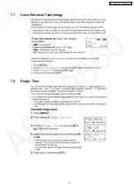
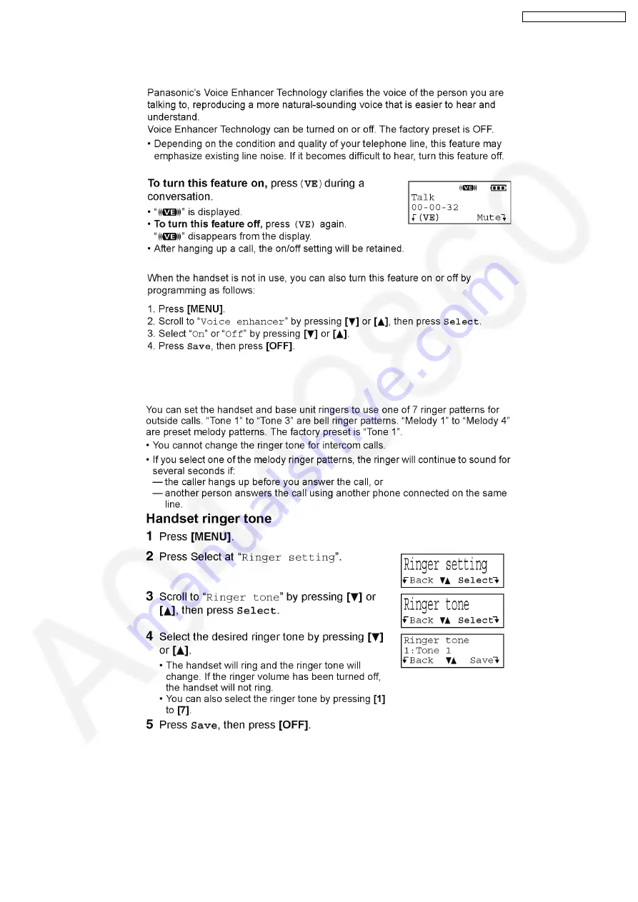
7.7. Voice Enhancer Technology

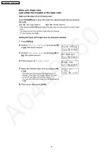
7.8. Ringer Tone

17

KX-TG2340JXS / KX-TGA236JXS

Summary of Contents for KX-TG2340JXS

Page 1: ... All rights reserved Unauthorized copying and distribution is a violation of law KX TG2340JXS KX TGA236JXS Digital Cordless Answering System Silver Version for Asia Middle Near East and Other Areas Telephone Equipment ORDER NO KM40505727CE ...

Page 2: ...Battery Charge 39 12 6 Check Link 40 12 7 Check the RF Part 41 12 8 Check Handset Transmission 45 12 9 Check Handset Reception 45 12 10 Check Caller ID 45 13 TEST MODE 46 13 1 Test Mode Flow Chart for Base Unit 46 13 2 Test Mode Flow Chart for Handset 49 13 3 X801 Base Unit X201 Handset Check 53 13 4 Adjust Battery Low Detector Voltage Handset 53 13 5 Base Unit Reference Drawing 54 13 6 Handset Re...

Page 3: ...LLATION PROCEDURE 81 24 4 BRIDGE MODIFICATION PROCEDURE 81 25 CABINET AND ELECTRICAL PARTS Base Unit 82 26 CABINET AND ELECTRICAL PARTS Handset 83 27 ACCESSORIES AND PACKING MATERIALS 84 28 TERMINAL GUIDE OF THE ICエS TRANSISTORS AND DIODES 85 28 1 Base Unit 85 28 2 Handset 85 29 REPLACEMENT PARTS LIST 86 29 1 Base Unit 86 29 2 Handset 88 29 3 Accessories and Packing Materials 90 30 FOR SCHEMATIC D...

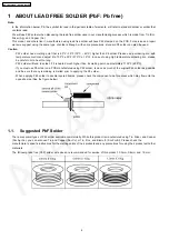
Page 4: ...eful not to heat too long PbF solder will tend to splash if it is heated much higher than its melting point approximately 1100 F 600 C If you must use Pb solder on a PCB manufactured using PbF solder remove as much of the original PbF solder as possible and be sure that any remaining is melted prior to applying the Pb solder When applying PbF solder to double layered boards please check the compon...

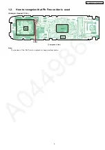
Page 5: ...ow to recognize that Pb Free solder is used Example Handset P C B IC901 IC201 IC202 PbF Marked Component View Note The location of the PbF mark is subject to change without notice 5 KX TG2340JXS KX TGA236JXS ...

Page 6: ...s boxes with aluminum foil 2 Ground the soldering irons 3 Use a conductive mat on the worktable 4 Do not touch IC or LSI pins with bare fingers 3 CAUTION Danger of explosion if battery is incorrectly replaced Replace only with the same or equivalent type recommended by the manufacturer Dispose of used batteries according to the manufacture s Instructions 6 KX TG2340JXS KX TGA236JXS ...

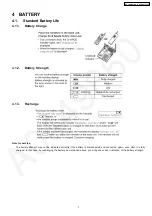
Page 7: ... Note for service The battery strength may not be indicated correctly if the battery is disconnected and connected again even after it is fully charged In that case by recharging the battery as mentioned above you will get a correct indication of the battery strength 7 KX TG2340JXS KX TGA236JXS ...

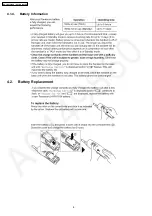
Page 8: ...4 1 4 Battery Information 4 2 Battery Replacement 8 KX TG2340JXS KX TGA236JXS ...

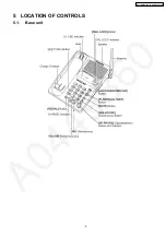
Page 9: ...5 LOCATION OF CONTROLS 5 1 Base unit 9 KX TG2340JXS KX TGA236JXS ...

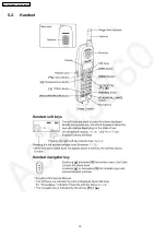
Page 10: ...5 2 Handset 10 KX TG2340JXS KX TGA236JXS ...

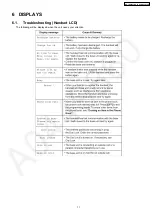
Page 11: ...6 DISPLAYS 6 1 Troubleshooting Handset LCD The following will be displayed when the unit needs your attention 11 KX TG2340JXS KX TGA236JXS ...

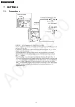
Page 12: ...7 SETTINGS 7 1 Connections 12 KX TG2340JXS KX TGA236JXS ...

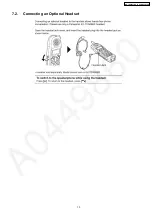
Page 13: ...7 2 Connecting an Optional Headset 13 KX TG2340JXS KX TGA236JXS ...

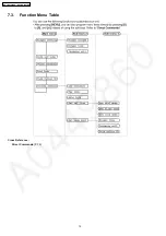
Page 14: ...7 3 Function Menu Table Cross Reference Direct Commands P 19 14 KX TG2340JXS KX TGA236JXS ...

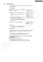
Page 15: ...7 4 Date and Time 15 KX TG2340JXS KX TGA236JXS ...

Page 16: ...7 5 Dialing Mode 7 6 Line Mode 16 KX TG2340JXS KX TGA236JXS ...

Page 17: ...7 7 Voice Enhancer Technology 7 8 Ringer Tone 17 KX TG2340JXS KX TGA236JXS ...

Page 18: ...18 KX TG2340JXS KX TGA236JXS ...

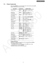
Page 19: ...7 9 Direct Commands 19 KX TG2340JXS KX TGA236JXS ...

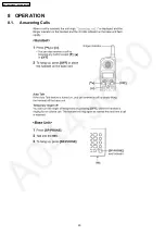
Page 20: ...8 1 Answering Calls 8 OPERATION 20 KX TG2340JXS KX TGA236JXS ...

Page 21: ...8 2 For Call Waiting Service Users 8 3 Using the PAUSE Key 21 KX TG2340JXS KX TGA236JXS ...

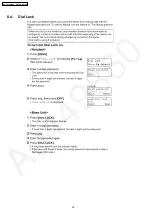
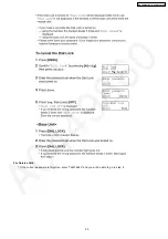
Page 22: ...8 4 Dial Lock 22 KX TG2340JXS KX TGA236JXS ...

Page 23: ...For Service Hint If the current password is forgotten enter 726276642 and you will be able to go to step 4 23 KX TG2340JXS KX TGA236JXS ...

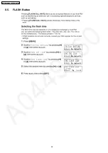
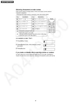
Page 24: ...8 5 FLASH Button 24 KX TG2340JXS KX TGA236JXS ...

Page 25: ...8 6 Phone Book 8 6 1 Storing Names and Numbers 25 KX TG2340JXS KX TGA236JXS ...

Page 26: ...26 KX TG2340JXS KX TGA236JXS ...

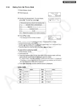
Page 27: ...8 6 2 Dialing from the Phone Book 27 KX TG2340JXS KX TGA236JXS ...

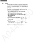
Page 28: ...8 6 3 Chain Dial 28 KX TG2340JXS KX TGA236JXS ...

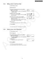
Page 29: ...8 6 4 Editing an Item in the Phone Book 8 6 5 Erasing an Item in the Phone Book 29 KX TG2340JXS KX TGA236JXS ...

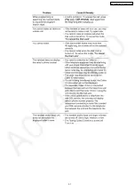
Page 30: ...e registering a Handset P 41 2 BATTERY P 7 3 Connections P 12 4 Dialing Mode P 16 5 Battery Charge P 7 6 Recharge P 7 7 Battery Replacement P 8 9 TROUBLESHOOTING Cross Reference 30 KX TG2340JXS KX TGA236JXS ...

Page 31: ...31 KX TG2340JXS KX TGA236JXS ...

Page 32: ... 8 Battery Charge P 7 9 Battery Replacement P 8 10 Recharge P 7 11 Date and Time P 15 12 Connecting an Optional Headset P 13 Cross Reference 32 KX TG2340JXS KX TGA236JXS ...

Page 33: ...10 DISASSEMBLY INSTRUCTIONS 10 1 Base Unit Shown in Fig To Remove Remove 1 Lower Cabinet Screws 2 6 14 A 5 2 Main P C Board Tape and Solder 3 Screws 2 6 8 B 8 33 KX TG2340JXS KX TGA236JXS ...

Page 34: ...andset Shown in Fig To Remove Remove 4 Rear Cabinet Screws 2 6 12 C 2 5 Follow the procedure 6 Main P C Board Tape and Solder 7 Screw 2 6 12 D 1 Screws 2 6 9 E 2 Charge Terminals 34 KX TG2340JXS KX TGA236JXS ...

Page 35: ...11 ASSEMBLY INSTRUCTIONS 11 1 Fix the LCD to P C Board Handset 35 KX TG2340JXS KX TGA236JXS ...

Page 36: ... Transmission P 38 Check Sp phone Reception P 38 Check Battery Charge P 39 Check Link P 40 Check the RF Part P 41 Check Handset Transmission P 45 Check Handset Reception P 45 Check Caller ID P 45 12 TROUBLESHOOTING GUIDE 36 KX TG2340JXS KX TGA236JXS ...

Page 37: ... not be done 1 Check the peripheral circuit of Flash Memory visually 2 Confirm that the voltage is added to the power supply pin If no voltage is detected replace the Flash Memory because it might be defect 3 Solder the Flash Memory again When the adjustment data was checked an error was detected The adjustment data may not be written Note Flash Memory is IC701 37 KX TG2340JXS KX TGA236JXS ...

Page 38: ...NAL ROUTE P 76 Cross Reference Telephone Line Interface P 68 SIGNAL ROUTE P 76 Note Flash Memory is IC701 DSP is IC501 Note Flash Memory is IC701 DSP is IC501 12 3 Check Sp phone Transmission 12 4 Check Sp phone Reception 38 KX TG2340JXS KX TGA236JXS ...

Page 39: ...Note DSP is IC501 12 5 Check Battery Charge 39 KX TG2340JXS KX TGA236JXS ...

Page 40: ...12 6 Check Link 1 Refer to Finding Out the Defective Part P 41 Cross Reference RF Check Flowchart P 42 40 KX TG2340JXS KX TGA236JXS ...

Page 41: ... 1 Finding Out the Defective Part After All the Checkings or Repairing Re register Handset to be checked to Base Unit to be checked and HS to BU Regular unit working 12 7 1 1 Re registering a Handset 41 KX TG2340JXS KX TGA236JXS ...

Page 42: ... 7 2 RF Check Flowchart Each item 1a 5 of RF Check Flowchart corresponds to Check Table for RF part Please refer to the each item Cross Reference Check Table for RF part P 43 42 KX TG2340JXS KX TGA236JXS ...

Page 43: ... 2 Set BU Regular Unit to TEST Link mode 1 CH 45ch TX Power High RX Gain High 3 Set HS to TEST Link mode 1 CH 45ch TX Power High RX Gain Low 4 Press 1 key of HS to establish link about 5m away from BU Regular Unit 5 Press 1 key of HS to set RSSI mode and press 2 key to set RX Gain Low 6 Confirm the value of RSSI in LCD of HS is more than e0 hex 2 Control signal confirmation 1 Set TX Burst mode 1 2...

Page 44: ...12 7 4 RF DSP interface signal wave form 44 KX TG2340JXS KX TGA236JXS ...

Page 45: ... Interface P 68 Calling Line Identification Caller ID P 70 Note Make sure the format of the Caller ID service of the Telephone company that the customer subscribed to Also we recommend to confirm that the customer is really a subscriber of the service 12 8 Check Handset Transmission 12 9 Check Handset Reception 12 10 Check Caller ID 45 KX TG2340JXS KX TGA236JXS ...

Page 46: ...13 TEST MODE 13 1 Test Mode Flow Chart for Base Unit 13 1 1 TX Burst Mode and Adjust X tal Mode 46 KX TG2340JXS KX TGA236JXS ...

Page 47: ...13 1 2 RX CW TEST Mode 47 KX TG2340JXS KX TGA236JXS ...

Page 48: ...13 1 3 Test Link Mode 48 KX TG2340JXS KX TGA236JXS ...

Page 49: ...13 2 Test Mode Flow Chart for Handset 13 2 1 TX Burst Mode 49 KX TG2340JXS KX TGA236JXS ...

Page 50: ...13 2 2 RX CW TEST Mode 50 KX TG2340JXS KX TGA236JXS ...

Page 51: ...13 2 3 Test Link Mode Note 1 LCD displays the Channel number exception default CH00 1ch 51 KX TG2340JXS KX TGA236JXS ...

Page 52: ... tal mode and Batt Low mode Cross Reference 1 Adjust Battery Low Detector Voltage Handset P 53 Note 2 These are the default values 3 These values may not be fixed depending on the battery strength 52 KX TG2340JXS KX TGA236JXS ...

Page 53: ...hecking tolerance 100Hz adjust to Adjustment tolelance 30Hz by pressing or key Adjustment Tolerance 13 824MHz 30Hz 5 Press TALK key to write the new frequency factor in EEPROM 6 Turn the power off Then this value is available Cross Reference Adjustment flow X tal mode and Batt Low mode P 52 13 4 Adjust Battery Low Detector Voltage Handset After handset s DSP IC201 or EEPROM IC202 replacement 1 Re ...

Page 54: ...81 R381 R164 D402 D161 D401 L402 L376 L377 D376 D377 L401 SP CHG YELLOW WHITE IC501 PbF IC701 DA101 Q150 C167 Q161 D404 C415 Q382 Q381 C315 D302 D301 Q202 IC201 L800 C802 L301 X801 C803 Q106 D103 Q104 Q105 CN101 LCD700 MIC C170 VCC FVCC RA702 KIN4 TTS1 RA701 INT0 UVCC2 URX2 UTX2 W_VDD IO1 JG2 IC300 JC2 JS2 JI2 JO2 FGND FRST BCK RSSI W_GND UGND2 TTS2 LGS1 LOUT1 Q103 C101 C102 IC901 C942 Q354 A N T ...

Page 55: ...LS ICOM R Y B G MICP1 MICM1 9 ANT1 ANTG1 LED721 LED722 LED724 R351 R352 R355 R356 Q570 Q301 R571 C570 R572 R300 C310 L302 C302 R301 R305 C301 C303 R303 C309 C304 R353 LED723 D306 D303 SPECTRUM ANALYZER ANT1 ANT1 ANTG1 DC 9V DC DCP DCM 1 DC VOLT METER ATT SG SG out AF VOLT METER OSCILLOSCOPE BELL SIMULATOR LOOP SIMULATOR Ring Tip L1R L1T Call_ID SIMULATOR FREQUENCY COUNTER 1 AF OSC AF OSC Flow Sold...

Page 56: ...Q205 Q206 IC205 IC203 Q212 D205 D206 Q208 Q209 Q210 Q204 C220 C213 RA201 X201 IC208 CHG1 CHG2 VSS VBAT RX TX VBAT2 VSS2 RST PDN MICM SPP RXI RSSI TXO DEMOD RECEIVER SP PHONE BCK SPM MICP VCC INT_0 VE_HK ANT ANT GND SSG FREQUENCY COUNTER 1 AC VOLT METER DC VOLT METER DC POWER SUPPLY MONITOR SP 8 OSCILLOSCOPE SPM SPP MIC_M MIC_P OSC 1 1kHz MIC LOAD 47 47 150 SPP SPM AC VOLT METER OSCILLOSCOPE VSS VB...

Page 57: ...72900 2438 183057 44 2439 266748 2439 076904 45 2440 156641 2439 966797 46 2441 050488 2440 860645 47 2441 940381 2441 750537 48 2442 834229 2442 644385 49 2443 724121 2443 534277 50 2444 617969 2444 428125 51 2445 507861 2445 318018 52 2446 401709 2446 211865 53 2447 291602 2447 101758 54 2448 185449 2447 995605 55 2449 075342 2448 885498 56 2449 969189 2449 779346 57 2450 859082 2450 669238 58 2...

Page 58: ...essages Stored phone numbers Caller list and etc This operation should not be performed for a usual repair 13 8 1 Base unit 13 8 2 Handset Note 1 Be sure to short the battery terminals of the handset with a lead wire etc for 2 seconds for discharge after removing the battery 58 KX TG2340JXS KX TGA236JXS ...

Page 59: ...cy The construction of RX TX frequency data is shown below It consists of 4 slots from the base unit to the cordless handset and 4 slots from the cordless handset to the base unit total 8 slots in 10ms By this slot system simultaneous air link and communication between 4 cordless handsets and the base unit can be realized One communication between cordless handset and the base unit is done by one ...

Page 60: ... UpLink4 is different frequency UpLink3 and DownLink3 use the same frequency 2 Handsets Link Traffic Bearer A link is established between Base set and handset The state where duplex communication is performed The hopping pattern of a 1800hops 18 seconds cycle Dummy Bearer The Base unit send Dummy data to the all stand by state Handsets The Handsets receive that data for keeping synchronization and...

Page 61: ...C201 The DSP performs TDD TDMA and ADPCM decoding to convert the RX DATA into the voice signal then it is output to the speaker Transmission The voice signal entering from the microphone is led to DSP IC201 The DSP encodes ADPCM and TDD TDMA with FHSS to TX DATA The TX DATA signal enters IC901 of RF UNIT and is modulated to 2 4GHz The RF signal is fed into Tx Rx switch D904 The RF signal is passed...

Page 62: ...15 EXPLANATION OF LINK DATA COMMUNICATION 15 1 Calling 15 2 To Terminate Communication 15 3 Ringing 62 KX TG2340JXS KX TGA236JXS ...

Page 63: ...IP HIN SPP SPN CHG_CTL CHG SO SI BCLK CS RESET IC501 DSP VBATT2 IC701 FLASH MEMORY VCC MIC SP IC301 Q301 D303 IC300 IC601 3 3V REGULATOR CHARGE DETECT CHARGE CONTROL 4 0V CONVERTOR 2 5V REGULATORS Q381 Q382 Q350 Q351 Q354 CHARGE_CONTACT Q104 Q161 Q150 RLY SIDE TONE CIRCUIT INUSE2 DETECT INUSE1 DETECT RECEIVE AMP D101 Q106 BELL DETECT CN101 DC_TEL JACK Tip Ring DC DC KX TG2340 BLOCK DIAGRAM Base Un...

Page 64: ...functions as follows 17 1 DSP Digital Speech Signal Processing IC501 17 1 1 Function Caller ID and Call Waiting CID demodulation The DSP implements monitor and demodulate the FSK signals that provide CID information from the Central Office Analog Switching The voice signal from Handset is transmitted to the speaker or the voice signal from Digital TAM System is transmitted to the Telephone line et...

Page 65: ...mory and initializes module 17 2 Flash Memory IC701 Following information data is stored Telephone number etc ex Telephone Directory number Caller ID data ID code Settings ex message numbers caller ID numbers pulse tone dial 17 3 Power Supply Circuit Function The power supply voltage from AC adaptor is converted to the desired voltage of each block Circuit Operation IC301 Q301 and D303 4 0V DCDC C...

Page 66: ...charge to prevent from overcharging Q381 and Q382 detect the ON HOOK state Handset is placed on base unit Q350 and Q351 control the charge current Q352 sends a signal to the handset for about 5 seconds soon after the handset is placed on the base unit This signal tells that the handset is been charging on the base unit When the signal is received charging on the base unit 66 KX TG2340JXS KX TGA236...

Page 67: ...en it incorporates an AC adaptor Circuit Operation When the AC Adaptor is inserted into the unit then the voltage is shifted by IC300 and power is supplied to the DSP The set starts to operate when VCC goes up to 3 3V or more in the circuit voltage diagram 67 KX TG2340JXS KX TGA236JXS ...

Page 68: ...le mode Q104 is open to cut the DC loop current and decrease the ring load When ring voltage appears at the Tip T and Ring R leads When the telephone rings the AC ring voltage is transferred as follows T L101 R130 C116 Q106 DSP pin 3 BELL When the CPU DSP detects a ring signal Q104 turns on thus providing an off hook condition active DC current flow through the circuit Following signal flow is the...

Page 69: ... hook by detecting changes in the T R voltage Circuit Operation Parallel connection detection when on hook When the set is on hook the voltage is monitored at DSP DCIN0 There is no parallel connection if the voltage is 2 50 V or higher while a parallel connection is deemed to exist if the voltage is lower Parallel connection detection when off hook When the set is off hook the voltage is monitored...

Page 70: ...The method is chosen according to the exchange of telephone office This unit is available to receive the data with both methods and displays the received data on LCD FSK Frequency Shift Keying format DTMF format It is the method to send the telephone number of calling party with DTMF to the telephone DTMF is sent before the first bell signal The data is sent in turn first the start code secondly t...

Page 71: ...BLOCK DIAGRAM Handset KX TGA236 BLOCK DIAGRAM Handset 2 5V VBATT2 3 0V IC205 D206 D213 D205 D208 D207 2 IC202 IC203 IC201 IC204 DI MOD_EN RXGAIN RSTN HSMIP HSMIN 1 INT_1 INT 1 71 KX TG2340JXS KX TGA236JXS ...

Page 72: ...eaning of the Motion of Pin 100 The period of Host Power Up Hardware Initialization In this period the host sets up some registers in order to wake up the system The period of Host Reset Software Initialization In this period the host reads the parameter from the memory and initializes module 19 1 2 RF unit Mainly voice signal is modulated to RF or it goes the other way 19 1 3 EEPROM IC202 All set...

Page 73: ... each block BATTERY 3 6V KEY BACK LIGHT RF UNIT REG 2 5V IC204 DSP LCD IC201 EEPROM IC202 MIC CIRCUIT 3 6V VBATT2 REG 3 0V IC203 Block Diagram Handset Power LEDS 3 0V BATT BATT CHARGE2 CHARGE1 D206 Q212 Q207 D213 D205 D208 D207 2 1 73 KX TG2340JXS KX TGA236JXS ...

Page 74: ...E2 and CHARGE1 flows D213 R248 Q207 pin80 of IC201 where the charge is detected Then IC201 calculates the battery consumption amount from the previous charge and it controls Q212 Q210 Q209 by pin82 of IC201 until charging is complete When charging is complete the control pattern is switched to Trickle charging form from Normal charging form 19 4 Ringer and Handset SP Phone 74 KX TG2340JXS KX TGA23...

Page 75: ... for the microphone is supplied from DSP 20 and the power is turned OFF on standby 19 6 Reception Signal The voice signal from the base unit is output to DSP 33 HSSPOUT This signal is led to the headset jack CN203 The signal through the headset jack and the other signal output from DSP 34 to drive the speaker When the headset is inserted to the jack the voice signal is cut at the jack so the sound...

Page 76: ...20 SIGNAL ROUTE Each signal route is as follows 76 KX TG2340JXS KX TGA236JXS ...

Page 77: ...62 GNDR GND Pin Description I O High High_Z Low 63 TXMOD A O 64 VREFR A O 65 RSSI A I 66 VCCR VCC 67 GNDPLL GND 68 VCCPLL VCC 69 XOUT A O 70 XIN A I 71 GND GND 72 Reset D I Normal Reset 73 Power Down D I Normal Power Down 74 FLASH_RST High Middle Low 75 TX_OUT D O High Low 76 MOD_EN D O Active Not 77 FLASH_SO High Middle Low 78 FLASH_SI High Middle Low 79 FLASH_CS High Middle Low 80 NC D O 81 RXEN...

Page 78: ...in the I O column means the port is controlled by the firmware Data in the blank columns are omitted because of the Analog I O Pin Description I O High High_Z Low 51 XOUT A O 52 XIN A I 53 GND GND GND 54 RESET D I Normal Reset 55 PDN D I Power On Power Down 56 FLASH _RESET D O Normal 57 TX OUT D O High Low 58 MOD_EN D O On Off 59 FLASH_SO D O Normal 60 FLASH_SI D O High Low 61 FLASH_CS D O Normal ...

Page 79: ...23 EXPLANATION OF IC TERMINALS RF Unit 23 1 IC901 79 KX TG2340JXS KX TGA236JXS ...

Page 80: ...pecific Gravity 0 82 Type RMA lower residue non cleaning type Note See ABOUT LEAD FREE SOLDER PbF Pb free P 4 24 2 FLAT PACKAGE IC REMOVAL PROCEDURE 1 Put plenty of solder on the IC pins so that the pins can be completely covered Note If the IC pins are not soldered enough you may give pressure to the P C board when cutting the pins with a cutter 2 Make a few cuts into the joint between the IC and...

Page 81: ...the corresponding soldering foil 2 Apply flux to all pins of the FLAT PACKAGE IC 3 Solder the pins sliding the soldering iron in the direction of the arrow 24 4 BRIDGE MODIFICATION PROCEDURE 1 Lightly resolder the bridged portion 2 Remove the remaining solder along the pins using a soldering iron as shown in the figure below 81 KX TG2340JXS KX TGA236JXS ...

Page 82: ...25 CABINET AND ELECTRICAL PARTS Base Unit 82 KX TG2340JXS KX TGA236JXS ...

Page 83: ...26 CABINET AND ELECTRICAL PARTS Handset 83 KX TG2340JXS KX TGA236JXS ...

Page 84: ...27 ACCESSORIES AND PACKING MATERIALS 84 KX TG2340JXS KX TGA236JXS ...

Page 85: ...28 TERMINAL GUIDE OF THE IC S TRANSISTORS AND DIODES 28 1 Base Unit 28 2 Handset 85 KX TG2340JXS KX TGA236JXS ...

Page 86: ...Z KEYBOARD SWITCH VM 13 PQSX10261V KEYBOARD SWITCH DIAL 14 PQMG10025Z RUBBER PARTS MIC COVER 15 PQKF10611Y1 CABINET COVER PS HB 16 PQHA10018Z RUBBER PARTS FOOT CUSHION 17 PQKL10061Z1 STAND WALL MOUNT PS HB 18 PQHA10017Z RUBBER PARTS LEG CUSHION 19 PQGT17697Z NAME PLATE 20 PQHR11032Z OPTIC CONDUCTIVE PARTS LED LENS 29 1 2 Main P C Board Parts Note 1 When you have replaced IC501 or IC701 adjust X801...

Page 87: ...101 100 R415 ERJ2GEJ222 2 2K R416 ERJ2GEJ222 2 2K R501 ERJ2GEJ102 1K R507 ERJ2GEJ102 1K Ref No Part No Part Name Description Remarks R516 ERJ2GEJ151 150 R543 ERJ2GEJ472X 4 7K R570 ERJ2GEJ473 47K R571 ERJ3GEYJ123 12K R572 ERJ3GEYJ102 1K R612 ERJ2GEJ101 100 R706 ERJ2GEJ104 100K R720 ERJ2GEJ271 270 R721 ERJ2GEJ271 270 R722 ERJ2GEJ181 180 R724 ERJ2GEJ391 390 R803 ERJ2GEJ182 1 8K R804 ERJ2GEJ151 150 R8...

Page 88: ...HB 102 PQGP10234Z1 PANEL LCD PC HB 103 PQHS10630Z TAPE DOUBLE SIDE 104 PQKE10373Z3 SPACER SPEAKER RING AS HB 105 PQHS10623Z TAPE DOUBLE SIDE 106 PQKM10628Z1 CABINET BODY ABS HB 107 PQGT18144Z NAME PLATE 108 PQSA10146X ANTENNA 109 PQHS10592Z SPACER SPEAKER 110 L0AD02A00020 SPEAKER 111 PQHS10634Z SPACER SPEAKER 112 PQHR10984Z GUIDE SPEAKER ABS HB 113 PQHS10624Z SPACER LCD CUSHION 114 L5DCBDC00009 LI...

Page 89: ...J2GEJ103 10K R247 ERJ2GEJ391 390 R248 ERJ2GEJ223 22K R249 ERJ2GEJ222 2 2K R260 ERJ2GEJ104 100K R263 ERJ2GEJ473 47K R264 ERJ2GEJ473 47K R266 ERJ2GEJ102 1K Ref No Part No Part Name Description Remarks R268 ERJ3GEYJ102 1K R269 ERJ3GEYJ102 1K R270 ERJ3GEYJ102 1K R275 ERJ2GEJ104 100K R276 ERJ2GEJ561 560 R277 ERJ2GEJ104 100K R279 ERJ2GEJ104 100K R284 ERJ2GEJ182 1 8K R285 ERJ2GEJ151 150 R286 ERJ2GEJ393X ...

Page 90: ...0EB1H102K 0 001 C984 ECUE1H1R5CCQ 1 5 S C990 ECJ0EB1H102K 0 001 C991 ECJ0EC1H100D 10P C992 ECJ0EC1H121J 120P C995 ECJ0EB1H102K 0 001 C993 F1G1A1040003 0 1 C995 ECJ0EB1H102K 0 001 C996 F1G1A1040003 0 1 OTHERS MIC L0CBAB000052 MICROPHONE E101 PQMC10471Z MAGNETIC SHIELD FRAME E102 PQMC10472Z MAGNETIC SHIELD COVER FL901 J0E2457B0008 LCR FILTER X201 H0J138500003 CRYSTAL OSCILLATOR 29 3 Accessories and ...

Page 91: ...2 This schematic diagram may be modified at any time with the development of new technology 30 2 Handset SCHEMATIC DIAGRAM Handset Notes 1 DC voltage measurements are taken with an oscilloscope or a tester with a ground 2 The schematic diagrams and circuit board may be modified at any time with the development of new technology 91 KX TG2340JXS KX TGA236JXS ...

Page 92: ... C804 C2P R801NC 13 824MHz X801 C805 C2P C554 K0 1 3P C809 1 8K R803 D404 NC 2 2K R415 R409 100 RA702 NC 1 3 5 7 8 6 4 2 DWN DWN UP UP SP SP NC C746 RINGER OFF FULL PAGER NC 1 2 3 4 5 6 7 8 9 10 11 12 C591 K0 1 LGS1 R802 NC RST INT0 C541 NC URX1 UTX1 R543 4 7K LED721 SP_LED R721 270 FVCC FGND FCS FSO FSI LED723 NC R723 NC C724 NC NC C701 NC C702 NC C703 NC C704 NC C705 NC C706 NC C707 NC C708 NC C...

Page 93: ...4 R K680P C112 CP1 CM1 C308 100u 25V C309 K0 1 R305 100 L302 22uH IC301 1 CE 2 GND 3 VOUT 4 EXT 5 VIN C311 47u 16V C310 K1 0 R127 1 0K Q301 SA104 NC NC SA103 D303 R571 12K R570 47K NC C570 R572 1K Q570 Q382 3 3K R381 15 R351 D351 NC D305 NC D301 NC D302 NC IC300 1 NC 2 RESET 3 VDET 4 VIN 5 VOUT 6 NC 7 GND 8 Cd Q105 NC C123 NC C122 NC 2 0V D161 C318 K0 1 C317 330u 6 3V NC C306 NC C307 NC C302 NC R3...

Page 94: ...RX_EN SHCTRL GND RF_RESET RSSI RX_DATA DMOD SDIO ANT RA201 4 7K 1 3 5 7 8 6 4 2 IC204 2 5V REG 1 OUT 3 GND 2 IN LED204 330 R203 LED202 330 R201 LED203 330 R204 330 R202 LED201 Q201 1 B1 2 E 3 B2 4 C2 5 C1 DEMOD TP_ANT RA207 220 2 4 6 8 7 5 3 1 C218K1 0 CA203 K0 1 8 6 5 7 4 2 1 3 CA202 K0 47 1 3 4 2 NC IC207 1 CD 2 VREF 3 VIN 4 VIN 5 VOUT1 6 VCC 7 GND 8 VOUT2 NC C320 NC C324 NC R320 NC R321 NC L320...

Page 95: ...C 74 SHCTRL 75 HEADSET_DET 76 TCK 77 TMS 78 TDI 79 TDO 80 CHARGE_DET 81 RF_RESET 82 CHARGE_CNT 83 KEYIN_5 84 KEYIN_4 85 KEYIN_3 86 KEYIN_2 87 KEYIN_1 88 KEY_LIGHT 89 LCD_BACK_LIGHT 90 NC 91 KEYSTROBE_E 92 KEYSTROBE_D 93 KEYSTROBE_C 94 KEYSTROBE_B 95 KEYSTROBE_A 96 GND 97 VCC 98 NC 99 FLASH_SCK 100 INT_1 NC R225 IC205 3 2V RESET OUT 1 VDD 2 NC 3 GND 4 C228 K0 1 Q208 270K R220 K470P C306 C309K0 1 R2...

Page 96: ...608 L901 4 7 R940 K0 1 C944 D10P C960 C1P C904 D10P C911 10R941 10 R942 K1000P C941 K0 1 C976 D10P C963 D10P C962 C1 5P C984 D10P C917 K0 01 C980 1K R931 1K R932 330 R933 NC C914 3 3nH L909 C2P C952 D10P C938 D10P C956 2 2nH L911 J220P C965 TP_TESTP TP_TESTN NC C994 0 R943 K1000P C990 D10P C991 1K R992 1K R991 K470P C937 K0 1 C993 NC C985 J120P C992 1uH 1608 L990 NC C920 D10P C903 K0 1 C996 C978 N...

Page 97: ... D161 D401 C421 C420 L402 L376 L377 D376 D377 L401 SP CHG YELLOW WHITE C143 C144 C133 R116 R109 C110 C160 R157 R155 C158 C124 R105 IC501 PbF IC701 R516 R711 C741 C742 C743 C744 C745 C746 C751 C750 C749 C748 C747 R506 R505 R710 R709 DA101 Q150 C167 Q161 D404 C415 Q382 Q381 C315 D302 D301 Q202 IC201 L800 C801 C802 C713 C509 C724 C723 C722 R706 R724 R723 R722 R507 C811 R806 C813 R333 R334 R501 R803 C...

Page 98: ...RDL DWN MIC LED720 JC1 JS1 JI1 JO1 UP SP UVCC1 UGND1 UTX1 URX1 HLD MUTE FLS ICOM R Y B G MICP1 MICM1 9 ANT1 ANTG1 LED721 LED722 LED724 R351 R352 R355 R356 Q570 Q301 R571 C570 R572 R300 C310 L302 C302 R301 R305 C301 C303 R303 C309 C304 R353 LED723 D306 D303 KX TG2340 CIRCUIT BOARD Flow Solder Side View Base Unit L1T ANT ANTG L1R DCM DCP KX TG2340JXS KX TGA236JXS 98 ...

Page 99: ... C960 C984 C983 RA901 C964 C995 C966 C965 C943 C946 C941 C993 C944 C942 C994 L990 C992 C985 FL901 L901 R903 C910 R992 R991 L904 L913 C911 C904 C913 D903 D904 C901 C912 L903 L909 C940 C939 L911 C918 C915 C921 C903 C920 C981 C914 R909 C996 C922 C991 C990 C952 C958 C957 C959 L905 L912 C938 L205 C322 C226 C229 R274 R277 R275 R220 R278 C205 C206 C209 L203 Q201 C291 C203 C204 R247 R234 C280 R230 C231 RA...

Page 100: ...WN MENU 1 2 3 4 5 6 7 8 LED203 LED204 LED201 LED202 9 0 SYA MIC HOLD FLASH REDIAL RIGHT LED208 Q213 R208 LED205 RA207 C211 R217 R218 C210 CA202 CA203 LED206 LED207 R201 R202 R203 R204 KX TGA236 CIRCUIT BOARD Flow Solder Side View Handset KX TG2340JXS KX TGA236JXS 100 ...

Page 101: ...101 KX TG2340JXS KX TGA236JXS M T N KXTG2340JXS KXTGA236JXS ...

Reviews: