background image

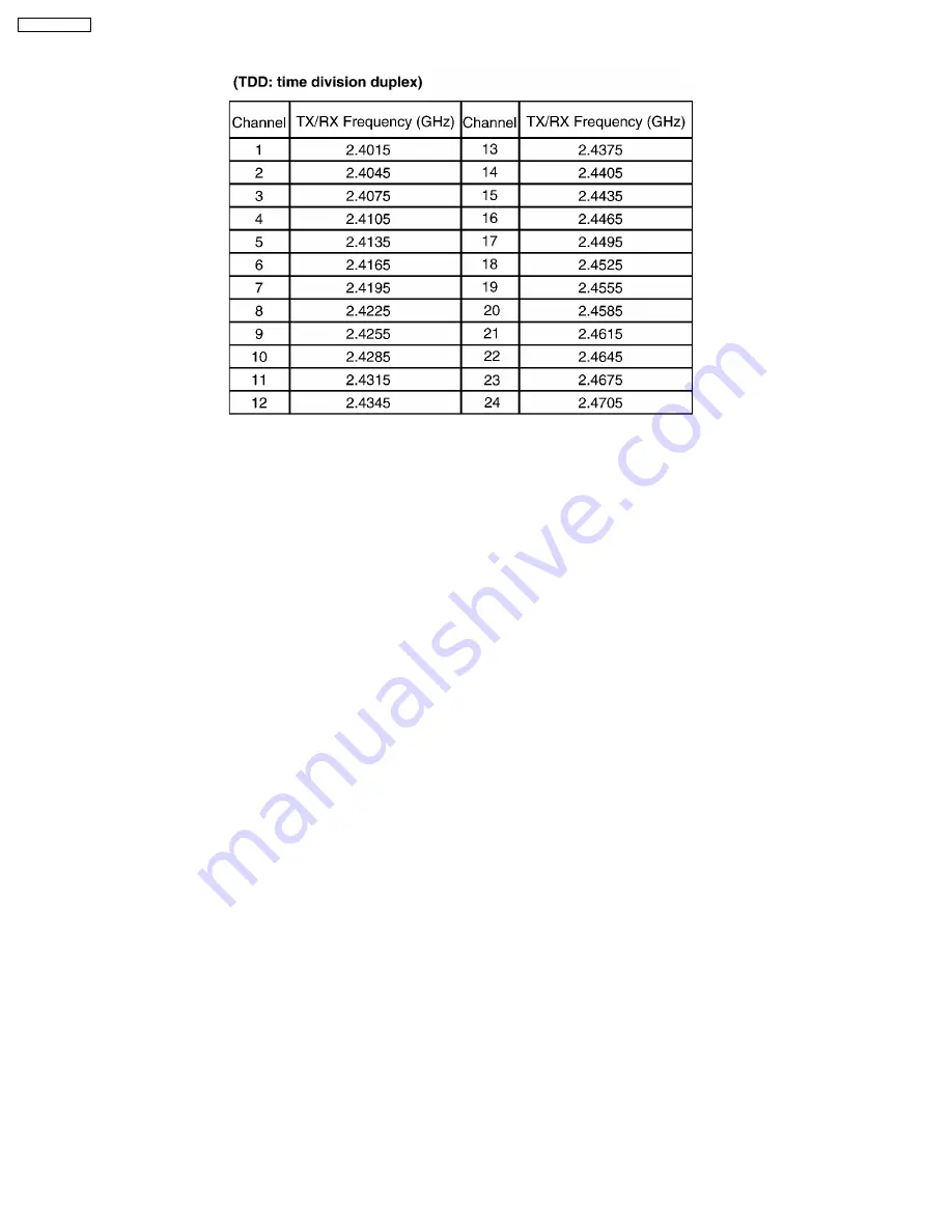
8.7. Frequency Table

50

KX-TG2559LBS

Summary of Contents for KX-TG2559LBS

Page 1: ...u Matsushita Electric Co Ltd All rights reserved Unauthorized copying and distribution is a violation of law KX TG2559LBS 2 4GHz Cordless System Silver Version for Brazil Telephone Equipment ORDER NO KM40107826C3 ...

Page 2: ...tage 46 8 4 Base Unit Reference Drawing 1 47 8 5 Base Unit Reference Drawing 2 48 8 6 Handset Reference Drawing 49 8 7 Frequency Table 50 9 DESCRIPTION 51 9 1 Frequency 51 9 2 Time Division Duplex TDD operation 51 9 3 Spread Spectrum 52 9 4 Signal Flowchart in the Whole System 53 9 5 EXPLANATION OF DSP DATA COMMUNICATION 54 10 TERMINAL GUIDE OF IC S TRANSISTORS AND DIODES 55 10 1 Base Unit 55 10 2...

Page 3: ... 2 Handset 77 22 3 ACCESSORIES AND PACKING MATERIALS 78 23 FOR SCHEMATIC DIAGRAM 79 23 1 Base Unit SCHEMATIC DIAGRAM Base Unit 79 23 2 Handset SCHEMATIC DIAGRAM Handset 79 23 3 MEMO 80 24 SCHMATIC DIAGRAM RF UNIT 81 24 1 Base Unit and Handset 81 25 SCHEMATIC DIAGRAM Base Unit 82 26 SCHEMATIC DIAGRAM Handset 84 27 CIRCUIT BOARD RF Unit 86 27 1 RF Unit Reference Drawing Base Unit and Handset 86 28 C...

Page 4: ...1 LOCATION OF CONTROLS 1 1 Base Unit 4 KX TG2559LBS ...

Page 5: ...1 2 Handset 5 KX TG2559LBS ...

Page 6: ...2 DISPLAY The handset shows you instructions and information on the display These display prompts are shown below 6 KX TG2559LBS ...

Page 7: ...7 KX TG2559LBS ...

Page 8: ...ic AC ADAPTOR PQLV17LBZ The AC adaptor must remain connected at all times It is normal for the adaptor to feel warm during use If you unit is connected to a PBX which does not support Caller ID services you cannot access those services 8 KX TG2559LBS ...

Page 9: ...3 2 Adding Another Phone 9 KX TG2559LBS ...

Page 10: ...3 3 STANDARD BATTERY LIFE 3 3 1 Battery Charge 3 3 2 Battery strength 3 3 3 Recharge 10 KX TG2559LBS ...

Page 11: ...3 3 4 Battery information 3 3 5 Standby mode The handset is off the base Unit 11 KX TG2559LBS ...

Page 12: ...3 4 Selecting the Dialing Mode 12 KX TG2559LBS ...

Page 13: ...3 5 Selecting the Line Mode 13 KX TG2559LBS ...

Page 14: ...4 OPERATION 4 1 Making Calls 14 KX TG2559LBS ...

Page 15: ...15 KX TG2559LBS ...

Page 16: ...4 2 Answering Calls 16 KX TG2559LBS ...

Page 17: ...4 3 Flash Button 17 KX TG2559LBS ...

Page 18: ...est call When the 51st call is received the first call is deleted Using the list you can automatically call back a caller You can store the caller s names and numbers from the Caller List into the directory The information at the handset display depends on the information sent by the telephone company Most of time the telephone company can send only the telephone numbers and it will not be able to...

Page 19: ...4 4 2 To check the number of new calls When new calls have been received the CALLER ID indicator flashes slowly on the base unit 19 KX TG2559LBS ...

Page 20: ...r list You can view the caller list with the handset Caller List information includes the caller s phone number and the number of times that caller called Make sure the handset is in the standby mode initially 20 KX TG2559LBS ...

Page 21: ...21 KX TG2559LBS ...

Page 22: ...4 4 4 Calling back from the caller list 22 KX TG2559LBS ...

Page 23: ... s phone number You can edit a phone number in the Caller List After editing the number you can continue with calling back or directory storing procedures Make sure the handset is in the standby mode initially 23 KX TG2559LBS ...

Page 24: ...4 4 6 Storing caller list information in the directory 24 KX TG2559LBS ...

Page 25: ...4 4 7 Erasing caller list information 4 4 8 To erase all entries in the Caller List 25 KX TG2559LBS ...

Page 26: ...5 DISASSEMBLY INSTRUCTIONS 26 KX TG2559LBS ...

Page 27: ...rd Remove the Main P C Board 3 3 3 Battery Cover Remove the Battery Cover 4 3 4 4 Rear Cabinet Screws 2 6 12 B 2 Screws 2 8 C 2 Screw 2 6 12 D 1 5 3 5 5 Antenna Screw 2 6 12 E 1 Main P C Board Screws 2 8 F 4 6 3 6 6 Main P C Board Pull the Charge Terminals outside Remove the Main P C Board 27 KX TG2559LBS ...

Page 28: ...6 ASSEMBLY INSTRUCTIONS 6 1 Assembly the LCD to P C Board Handset 28 KX TG2559LBS ...

Page 29: ...6 2 How To Check Splash Resistance 29 KX TG2559LBS ...

Page 30: ...move solder on six legs of RF unit 3 Remove solder on all pads of RF unit 4 Replace defective RF unit with new HS RF unit NOTE Do not use BU RF unit for HS one HS RF unit is different from BU one 5 Solder all pads of RF unit 6 Solder six RF legs 7 Put LCD unit and solder speaker wire NOTE Speaker wire has polarity Component View Solder Side View 30 KX TG2559LBS ...

Page 31: ...7 TROUBLESHOOTING GUIDE 31 KX TG2559LBS ...

Page 32: ...7 1 Check Power 32 KX TG2559LBS ...

Page 33: ...7 2 Check Battery Charge NOTE CP CM Refer to Base Unit Reference Drawing 1 TP BL Refer to Handset Reference Drawing 33 KX TG2559LBS ...

Page 34: ...7 3 Check Link 34 KX TG2559LBS ...

Page 35: ... Power Normal mode The switch of Test Fixture changed with Normal mode side Then Test Fixture is in Normal mode NOTE Audio is coming from Receiver whether switch is TEST mode or Normal mode This test simulates the handset is at very large distance from the base unit and the TX signal from handset to base is very small Procedure First place handset Test Fixture on base under test to charge exchange...

Page 36: ...awing As for TEST fixture only the switch as shown in figure is connected to mass production set B E C RF UNIT SW OFF Normal Mode SW ON TEST Mode Handset GND SW S_LOW NOTE SW ON Base Unit Normal 10 m more No Link 5 m less Link 36 KX TG2559LBS ...

Page 37: ...h is inserted or not This test simulates the handset is at very large distance from the base unit and the TX signal from base to handset is very small Procedure First place handset under test to charge exchange security code then remove handset from base after you hear a beep Press TALK button on handset and if it links with the base then this handset sensitivity is OK If a beep is not heard Repla...

Page 38: ... only the switch as shown in a figure is connected to the mass production set RF UNIT G601 G602 G603 G604 G605 G606 B C E B C E B C E SW OFF Normal Mode SW ON TEST Mode Base Unit GND SW S_LOW Note SW ON Portable Unit Normal 10m more No Link 5m less Link 38 KX TG2559LBS ...

Page 39: ...tem 1a 6 of RF Check Flowchart is corresponded to Check Table for RF Block Please refer each item one by one 1 See RF Unit Reference Drawing Base Unit and Handset 2 Base unit RF only refer to Check Table for RF Block 39 KX TG2559LBS ...

Page 40: ...y within 24MHz 720Hz at TP_FREQ 4 of RF Unit If X101 frequency is spec out than adjust frequency within 24 MHz 100 Hz by VC101 1 Set HS to Test STANDBY mode 5 2 Confirm X101 frequency within 24MHz 720Hz at TP_FREQ 4 of RF Unit If X101 frequency is spec out than adjust frequency within 24 MHz 100 Hz by VC101 3 TX Pow_Low confirmation 1 Put low loss high frequency wire to ANT1 2 and GND 2 2 Connect ...

Page 41: ...7 4 6 RF DSP Interface Signal Wave Form 41 KX TG2559LBS ...

Page 42: ...7 5 Check Handset Voice Transmission 7 6 Check Handset Voice Reception 42 KX TG2559LBS ...

Page 43: ...7 7 Check Call ID 43 KX TG2559LBS ...

Page 44: ...8 TEST MODE AND ADJUSTMENT 8 1 Test Mode Flow Chart for Base Unit 1 See Base Unit Reference Drawing 1 2 Special check method for Base Unit individually 44 KX TG2559LBS ...

Page 45: ...8 2 Test Mode Flow Chart for Handset 1 See Handset Reference Drawing 2 Special check method for Handset individually 45 KX TG2559LBS ...

Page 46: ... this adjustment 1 Set 3 9V for DC power supply 2 Place handset in test mode 3 Press TALK key 4 times to TX Low mode CW Tx Low is displayed on LCD 4 Set 3 51V for DC power supply Check voltage at battery connector because some voltage drop is happened using long or thin cable 5 Press key to write voltage value in EEPROM 6 Turn power off Then this value is available NOTE Refer to Handset Reference ...

Page 47: ... 1 IC551 B E C B E C DC 9V ANT 2 ANT 1 SA FREQUENCY_COUNTER 24MHz 720Hz TP_FREQ RF_UNIT LOCATOR CDL TEST MODE SW Bell SIMULATOR AF VOLT METER LOOP SIMULATOR Call ID SIMULATOR 400Ω 600Ω LB OSC CM CP AF OSC 25dBm 1 1kHz KX TG2559LBS 47 ...

Page 48: ...8 5 Base Unit Reference Drawing 2 RF UNIT G601 G602 G603 G604 G605 G606 IC571 IC501 E C B E C B E C B E C B B C E B C E B C E IC301 KX TG2559LBS 48 ...

Page 49: ...kHz 600Ω 45dBm f 1 1 kHz MIC_M MIC_P TP_VBAT TP_VSS 3 9V OSCILLOSCOPE AC VOLT METER 150W 50W CABLE 150W OSC 1 1kHz OPEN SPM SPP TEST TP_VCC TP_BL MIC1 SP1 AC VOLT METER 10m OSCILLOSCOPE HAND SET HEAD SET ANTG ANT Spectrum Analyzer FREQUENCY COUNTER TP_FREQ 24MHz 720Hz No 1 Confirm Frequency Volt meter KX TG2559LBS 49 ...

Page 50: ...8 7 Frequency Table 50 KX TG2559LBS ...

Page 51: ... in transmitting between the base unit and handset Fig 7 9 2 1 TDD Frame Format The TDD frame is 2mS in length and is composed of two symmetrical 960 µS TX and RX subframes Each subframe contains 96 bits of 10µS duration with 40µS guard times between both TX and RX subframes Each subframe consists of the following five fields A 12 bit Preamble field An 8 bit Data Channel field An 8 bit Sync Word A...

Page 52: ...ctrum method DSS Digital Spread Spectrum Mixing the original signal with the pseudo random noise code PN code works the spread spectrum In this system PN code is 15 chip Although the band width is spread fifteen times the power level per channel becomes lower Fig 8 52 KX TG2559LBS ...

Page 53: ...er L107 and the balun T101 to perform the de spread then input to DSP IC201 DSP performs ADPCM decoding to convert the signal into the voice signal then it is output to the speaker Transmission The voice signal input from the microphone is led to DSP IC201 The DSP generates ADPCM signal As well as the reception it is converted into the RF signal by RFIC IC101 Passing through the balun T101 and fil...

Page 54: ...9 5 1 Calling 9 5 2 To Terminate Communication 9 5 3 Ringing 9 5 4 ID CHANGE 9 5 EXPLANATION OF DSP DATA COMMUNICATION 54 KX TG2559LBS ...

Page 55: ...10 TERMINAL GUIDE OF IC S TRANSISTORS AND DIODES 10 1 Base Unit 10 2 Handset 55 KX TG2559LBS ...

Page 56: ...11 BLOCK DIAGRAM Base Unit Q371 Q311 Q621 7V 7V Q601 Q343 Q461 Q115 3 6V 3 6V VPWR VRF1 VRF2 PCONT REGULATOR Q611 S LOW IC551 EEP ROM DATA CS CLK RF_RESET BBIC_PWDN RIGHT ANT1 LEFT ANT2 KX TG2559LBS 56 ...

Page 57: ...power supply The voltage at point A is regulated to 4 5 V by IC301 The voltage at point B is dropped by D509 to 4 1 V The voltage at point C is dropped by D521 to 3 8 V The voltage at point E is dropped by Q601 to 3 6V 12 2 DTMF Signal When the DTMF data from the Handset is received the DTMF signal is output from pin 36 of IC501 and sent to the line through Q131 57 KX TG2559LBS ...

Page 58: ...ded by IC501 The audio signal output from IC501 36 and is input to telephone line 12 4 Line Receiving Signal The audio signal from line passes through Q131 and Q461 to pin38 and 39 of IC501 DSP IC501 modulates this input audio signal to output to the RF unit 58 KX TG2559LBS ...

Page 59: ...r ID service contract has been entered for the circuit being used This model can receive 2 types of Caller ID FSK type DTMF type FSK type The data for the caller ID from the telephone exchange is sent during the interval between the first and second rings of the bell signal The data from the telephone exchange is a modem signal which is modulated in an FSK Frequency Shift Keying format Data 0 is a...

Page 60: ...60 KX TG2559LBS ...

Page 61: ...r off hook by detecting changes in the T R voltage Circuit Operation Parallel connection detection when on hook When on hook Q115 is ON the voltage is monitored pin 40 of IC501 There is no parallel connection if the voltage is 1 65 V or higher while a parallel connection is deemed to exist if the voltage is lower Parallel connection detection when off hook When off hook Q115 is OFF the voltage is ...

Page 62: ...nt flow through the circuit and the following signal flow is for the voice signal T D101 Q121 Q131 R139 R140 C139 RX ON HOOK Q121 is open Q121 is connected as to cut the DC loop current and to cut the voice signal The unit is consequently in an on hook condition SPECIFICATIONS In the on hook state idle the current flows between the telephone line and the unit is as follows T L101 R103 C103 R106 C1...

Page 63: ... power is supplied to the DSP The set can operate beyond point A in the circuit voltage diagram 12 9 Antenna Diversity Antenna Diversity improve conversation quality This means to reduce some noise during conversation RF unit send LQA Link Quality Alarm signal to IC751 when increase Error Bit s Then IC751 control RF switch IC761 to switch another Antenna Antenna selection control by IC501 is avail...

Page 64: ...3V IC203 Block Diagram Handset Power RF UNIT LEDS 3 3V BATT BATT D214 D216 CHARGE2 CN202 CHARGE1 Q203 Q211 CN202 14 2 Charge Circuit Ni cd battery is connected to CN202 When the handset is put on the cradle of the base unit the power is supplied from CHARGE1 and CHARGE2 terminals to charge the battery Q207 detects the voltage of CHARGE1 and CHARGE2 terminals then the handset makes ID code setting ...

Page 65: ... Sending Signal The voice signal from the microphone input to pin 42 CIDIP and pin 41 CIDIN of IC201 DSP CN203 is the headphone jack When the headphone is connected the Q206 detect it The input from the microphone of the handset CIDIN CIDIP is cut and the microphone signal from the headphone is input to pin 47 of IC201 HMIN Also the power for the microphone is supplied from Q211 and the power is t...

Page 66: ...f IC201 DSP as the voice signal SPN is the inverse output of SPP and the speaker is driven by SPN and SPP CN203 is the headphone jack When the headphone is connected to this jack the output to the speaker of the handset SPN SPP is cut and the voice signal is output to the headphone HSOUT only 67 KX TG2559LBS ...

Page 67: ...15 CPU DATA Base Unit 15 1 IC501 68 KX TG2559LBS ...

Page 68: ...16 CPU DATA Handset 16 1 IC201 69 KX TG2559LBS ...

Page 69: ...17 EXPLANATION OF IC TERMINALS RF Unit Base Unit 17 1 IC101 70 KX TG2559LBS ...

Page 70: ...flux will be replaced daily 18 2 Procedure 1 Temporary fix FLAT PACKAGE IC by soldering on two marked 2 pins Most important matter is accurate setting of IC to the corresponding soldering foil 2 Apply flux for all pins of FLAT PACKAGE IC 3 Solder employing specified solder to direction of arrow as sliding the soldering iron 18 3 Modification Procedure of Bridge 1 Re solder slightly on bridged port...

Page 71: ...19 CABINET AND ELECTRICAL PARTS Base Unit 72 KX TG2559LBS ...

Page 72: ...20 CABINET AND ELECTRICAL PARTS Handset 73 KX TG2559LBS ...

Page 73: ...21 ACCESSORIES AND PACKING MATERIALS 74 KX TG2559LBS ...

Page 74: ...BOARD PARTS Ref No Part No Part Name Description Remarks PCB1 PQWPG2559LBH MAIN P C BOARD ASS Y RTL ICS IC301 PQVIXCF4502P IC S IC331 PQVIPS3432UT IC S IC501 C2HBBJ000007 IC IC551 PQWIG2559LBH IC IC741 PQVITC7S08FU IC S IC751 PQVITC7W74U IC S IC761 PQVISPM3204T IC S TRANSISTORS Q101 2SD1819A TRANSISTOR SI Q115 2SD1819A TRANSISTOR SI Q121 2SA1625 TRANSISTOR SI S Q122 PQVT2N6517CA TRANSISTOR SI S Q1...

Page 75: ...J151 150 R448 ERJ3GEYJ222 2 2k R449 ERJ3GEYJ102 1k R451 ERJ3GEYJ103 10k R461 ERJ3GEYJ150 15 R462 ERJ3GEYJ392 3 9k Ref No Part No Part Name Description Remarks R464 ERJ3GEYJ474 470k R465 ERJ3GEYJ390 39 R516 ERJ3GEY0R00 0 R521 ERJ3GEY0R00 0 R541 ERJ3GEYJ151 150 R542 ERJ3GEYJ331 330 R543 ERJ3GEYJ471 470 R546 ERJ3GEYJ472 4 7k R551 ERJ3GEYJ274 270k R553 ERJ3GEYJ103 10k R554 ERJ3GEYJ103 10k R559 ERJ3GEY...

Page 76: ... PQKE10128Z1 EARPHONE CAP S 122 PQKE10129Z1 COVER S Ref No Part No Part Name Description Remarks 123 PQP510SVC BATTERY S 124 PQQT22262Z CHARGE LABEL 125 PQSA10120U ANTENNA 126 PQSX10171Z RUBBER SWITCH 127 PQKF10514Z2 LOWER CABINET S 128 PQKK10117Z2 BATTERY COVER S 129 PQHG10629Z RUBER BATTERY 130 PQYMG2553BXS FRONT CABINET ASS Y 22 2 2 MAIN P C BOARD PARTS Ref No Part No Part Name Description Rema...

Page 77: ...04KBV 0 1 C210 ECUV1C104KBV 0 1 C211 ECUV1A474KBV 0 47 C212 ECUV1A474KBV 0 47 C213 ECEV1AA221 220 C214 ECUV1H103KBV 0 01 C215 ECUV1A474KBV 0 47 C217 ECUV1C104ZFV 0 1 C218 ECUV1C104ZFV 0 1 C219 ECUV1H470JCV 47p C220 ECEV0JA101 100 C221 ECUV1C104ZFV 0 1 C222 ECUV1C104ZFV 0 1 C223 ECST0JY106 10 C224 ECUV1C104ZFV 0 1 C226 ECUV1C104ZFV 0 1 C227 ECUV1H470JCV 47p C228 ECUV1C104ZFV 0 1 C229 ECUV1C104ZFV 0...

Page 78: ... line 2 This schematic diagram may be modified at any time with the development of new technology 23 2 Handset SCHEMATIC DIAGRAM Handset Notes 1 DC voltage measurements are taken with an oscilloscope or a tester with a ground 2 The schematic diagrams and circuit board may be modified at any time with the development of new technology 79 KX TG2559LBS ...

Page 79: ...23 3 MEMO 80 KX TG2559LBS ...

Page 80: ...24 SCHMATIC DIAGRAM RF UNIT 24 1 Base Unit and Handset IC110 IC105 IC113 IC112 IC109 IC114 IC101 IC106 KX TG2559LBS 81 ...

Page 81: ...MATIC DIAGRAM Base Unit RF Signal NC NC ATN DVC IC501 IC571 IC751 IC741 IC761 IC551 TALK TX TALK RX 3 5V 3 7V 26mVp p TX High power Level 20 4dBm 2 4015 2 4705GHz 1 4 7 18 19 20 26 27 8 17 2 3 82 KX TG2559LBS ...

Page 82: ... 1kHz 140mVp p 25dBm 600 Output 420mVp p 13dBm 60mVp p 20mVp p 16mVp p 22mV p p 400mVp p 4 1V 3 8V 4 1V 6 8V 4 5V 4 1V 11 0V 7 4V 4 0V 3 7V 1 4 7 18 19 20 26 27 8 17 2 3 TG2559LBS SCHEMATIC DIAGRAM Base Unit 83 KX TG2559LBS ...

Page 83: ...EMATIC DIAGRAM Handset IC202 TX H S RX H S TX Normal RX Normal TX High power Level 20 4dBm 2 4015 2 4705GHz RF SIGNAL 1 2 3 15 29 4 14 32 36 39 40 37 38 41 43 44 46 50 52 53 55 47 48 49 30 31 84 KX TG2559LBS ...

Page 84: ...KEY_STROB EGPIO8 KEY_STROB EGPIO9 KEY_STROB NC SPI_DOUT SPI_EN SPI_CLK GND SPI_DIN 30 ALARM_VOL NC CD12 CD13 CD14 CD15 VCC GND RF_RESET ADPCM_IN ADPCM_OUT ADPCM_SYNC ADPCM_BCLK LIGHTED_LED NC NC LCD_B L HEADSET NC NC NC NC IRQ_TXRX NC PDN RESET GND XIN XOUT VRTC VCCPLL GNDPA SPP SPN VCCPA HSOUT LOUT VCCA LIN LGS DCIN CIDIN CIDIP CIDO HMGS HMIN GNDA MIN MGS VREF GNDPLL CHG S_LOW PCONT NC NC NC NC N...

Page 85: ...88 C157 C146 L115 C178 C161 C130 C185 L110 R150 C134 R117 R149 R116 C133 R122 R154 R114 R147 C128 C124 R143 R111 C125 R144 R145 C126 R146 R155 C122 R151 C132 R148 C131 C196 R126 C115 C114 C143 R121 R107 R108 R109 R110 R131 C127 R120 R105 R115 R130 R139 C184 C150 C149 R128 C162 C167 R129 C106 VC101 X101 IC106 IC110 L106 C111 C144 C110 R101 R104 C152 C112 C103 C140 R102 C118 R158 R157 C119 R153 C190...

Page 86: ...28 CIRCUIT BOARD Base Unit 28 1 Component View RF UNIT G601 G602 G603 G604 G605 G606 IC571 IC501 E C B E C B E C B E C B B C E B C E B C E IC301 IC331 IC751 IC761 IC741 KX TG2559LBS 87 ...

Page 87: ...28 2 Flow Solder Side View IC551 B E C B E C KX TG2559LBS 88 ...

Page 88: ...29 CIRCUIT BOARD Handset 29 1 Component View IC201 E B C E B C E B C E B C E B C E B C B E C B E C IC202 E B C B E C RF UNIT IC204 IC203 IC205 KX TG2559LBS 89 ...

Page 89: ...INE2 CONF TALK UP DIRECT LEFT FUNC EXIT DOWN 1 2 3 4 5 6 7 8 LED203 R203 LED204 R204 9 0 SYA RDL PAUSE FLS CWIT RIGHT INT CLEAR R205 R206 C215 C212 R272 C297 C298 E B C R207 Q203 R261 R262 C211 R217 C210 C209 C208 C207 C206 R218 LED201 R201 LED202 R202 KX TG2559LBS 90 ...

Page 90: ...91 KX TG2559LBS M H KXTG2559LBS Printed in Japan ...

Reviews: