background image

51

KX-TG2853BXS/KX-TG2854BXS/KX-TGA280BXS

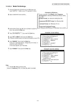
12.3.2.2. Batch file Settings

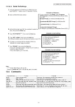
Note:

• “****” varies depending on the country.
• Refer to 

Commands

 (P.51) for frequently used commands.

12.4. Commands

Command name

Function

Example

getver

Check software version

Type “getver”, then registered software version is read out.

readid

Read ID (RFPI)

Type “readid”, then registered ID is read out.

bandgap

Check VDD adjustment parameter value

Type “bandgap”, then registered bandgap adjust value is read out.

bandgap nn

Set VDD voltage adjustment parameter value Type “bandgap nn”, nn is an adjustment setting value of the bandgap voltage.

conttx

Set RFC (burst mode)

Type “conttx”, then set RF-burst mode.

setfreq

Check frequency adjustment parameter value Type “setfreq”, then registered freq adjustment value is read out.

setfreq nn

Set frequency adjustment parameter value

Type “setfreq nn”, nn is an adjustment setting value of the frequency. 

eeprom_hs_init

Set default data to the EEPROM (handset) 

Type “eeprom_hs_init”, then default data is registered.

Summary of Contents for KX-TG2853BXS

Page 1: ...d distribu tion is a violation of law ORDER NO KM40607144CE Telephone Equipment KX TG2853BXS KX TG2854BXS KX TGA280BXS Expandable Digital Cordless Answering System Expandable Digital Cordless Answering System with Two Handsets Silver Version for Asia Middle Near East and Other areas ...

Page 2: ...2 KX TG2853BXS KX TG2854BXS KX TGA280BXS ...

Page 3: ...oting by Symptom Base Unit 40 10 3 How to Replace the Flat Package IC 41 11 Disassembly and Assembly Instructions 43 11 1 Disassembly Instructions 43 11 2 Fix the LCD to the Main P C Board Handset 46 12 Measurements and Adjustments 47 12 1 Things to Do after Replacing IC 47 12 2 The Setting Method of JIG Base Unit 48 12 3 The Setting Method of JIG Handset 50 12 4 Commands 51 12 5 Adjustment of Han...

Page 4: ...ts will refer to standard solder or solder that con tains lead We will use PbF solder when discussing the lead free solder used in our manufacturing process which is made from Tin Sn Silver Ag and Copper Cu This model and others like it manufactured using lead free solder will have PbF stamped on the PCB For service and repair work we suggest using the same type of solder Caution PbF solder has a ...

Page 5: ... Please check the manufacturer s specific instructions for the melting points of their products and any precautions for using their product with other materials The following lead free PbF solder wire sizes are recommended for service of this product 0 3 mm 0 6 mm and 1 0 mm 2 2 2 How to Recognize that Pb Free Solder is Used Example Handset P C B Component View Note The location of the PbF mark is...

Page 6: ...6 KX TG2853BXS KX TG2854BXS KX TGA280BXS 3 Specifications ...

Page 7: ...OK Off Hook Line Voltage D A A D ADPCM Codec Filter DSP Speech Decoding Speech Encoding BMC Burst Decoding Burst Encoding RF Interface IC701 RXDA ANT1 ANT2 TXDA RSSI SYCL SYDA SYEN RF Module XTAL X1 10 368 MHz SP AMP IC402 Flash Memory IC501 To AC Adaptor CN301 Limit Resistor CHARGE CONTACT 3 45V Reg IC301 3 0V Reg Q2 1 8V Reg Q3 3 45V 3 0V 1 8V Bell Interface IC1 BBIC KX TG2853 2854 BLOCK DIAGRAM...

Page 8: ...eration for RF Module ADC DAC timer and power control circuitry All interfaces ex RF module LED Analog Front End etc RF Module IC701 Transceiver IC including LNA PLL demodulator logic PA TX power amplifier FLASH MEMORY IC501 Voice Prompt TAM D L Area Additionally Power Supply Circuit 3 45V 3 0V 1 8V output Crystal Circuit 10 368MHz Charge Circuit Telephone Line Interface Circuit 4 2 2 Power Supply...

Page 9: ...n The Clip signal voltage is transferred as follows A C121 R123 R128 IC1 Pin 112 CIDinn B C131 R133 R138 IC1 Pin 107 CIDinn ON OFF hook circuit In the standby mode Q104 is open and connected as to cut the DC loop current and to cut the voice signal The unit is conse quently in an on hook condition When IC1 detects a ring signal or press the TALK Key onto the handset Q105 turns on and Q104 turns on...

Page 10: ...set Receiver RF_UNIT IC700 ANT X1 10 368 MHz EEPROM IC2 LCD Speaker Charge Control Q500 Q501 Q502 LCD_Light LED2 3 4 Q101 D501 ANT_LED KEY_Light LED5 6 7 8 Q100 Power Circuit IC300 IC301 Q300 Q301 Q302 MIC Charge Battery BBIC IC1 KEYS KX TGA280 BLOCK DIAGRAM Handset ...

Page 11: ... DSP and RF part as shown in the block diagram 4 4 1 1 BBIC IC1 Function Battery Low Power down detect circuit Ringer Generation Interface circuit RF part Speaker Mic LED Key scan LCD Initial waves 4 4 1 2 RF part Mainly voice signal is modulated to RF or it goes the other way 4 4 1 3 EEPROM IC2 ALL setting data is stored ...

Page 12: ...X TG2853BXS KX TG2854BXS KX TGA280BXS 4 4 2 Power Supply Circuit Circuit Operation When power on the handset the voltage is as follows BATTERY 2 2 V 2 6 V J1 L502 L300 D300 Q300 3 4 V Q302 1 8 V Q301 2 5 V ...

Page 13: ...current is as follows DC 6 5V R304 R305 R309 R310 CHARGE Base CHARGE Handset Q502 D501 L502 BATTERY Battery BATTERY L503 GND R504 CHARGE Handset CHARGE Base GND DC GND In this way the BBIC on handset detects the fact that the battery is charged The charge current is controlled by switching Q500 of handset 4 4 4 Ringer and Handset SP phone ...

Page 14: ...cted by BBIC which check the voltage from battery The detected voltage is as follows Battery Low Battery voltage V Batt 2 3V 50mV The BBIC detects this level and starts flashing Power Down Battery voltage V Batt 2 1V 50mV The BBIC detects this level and power down 4 5 Circuit Operation Charger Unit 4 5 1 Power Supply Circuit The power supply is as shown ...

Page 15: ...15 KX TG2853BXS KX TG2854BXS KX TGA280BXS 4 6 Signal Route ...

Page 16: ...16 KX TG2853BXS KX TG2854BXS KX TGA280BXS 5 Location of Controls and Components 5 1 Controls 5 1 1 Base Unit ...

Page 17: ...17 KX TG2853BXS KX TG2854BXS KX TGA280BXS 5 1 2 Cordless Handset 5 1 3 Charger 5 2 Display ...

Page 18: ...18 KX TG2853BXS KX TG2854BXS KX TGA280BXS 6 Installation Instructions 6 1 Connections ...

Page 19: ...19 KX TG2853BXS KX TG2854BXS KX TGA280BXS 6 2 Battery Installation Replacement 6 3 Battery Charge ...

Page 20: ...20 KX TG2853BXS KX TG2854BXS KX TGA280BXS 6 3 1 Battery Strength 6 3 2 Recharging the Battery 6 3 3 Battery Performance ...

Page 21: ...21 KX TG2853BXS KX TG2854BXS KX TGA280BXS 7 Operation Instructions 7 1 Guide to Cordless Handset Programming 7 1 1 Programming by Scrolling through the Display Menus ...

Page 22: ...22 KX TG2853BXS KX TG2854BXS KX TGA280BXS 7 1 2 Programming Using the Direct Commands ...

Page 23: ...23 KX TG2853BXS KX TG2854BXS KX TGA280BXS 7 2 Dial Lock For Service Hint If the current password is forgotten enter 726276642 and you will be able to go to the next step ...

Page 24: ...24 KX TG2853BXS KX TG2854BXS KX TGA280BXS 7 3 Registering the Cordless Handset 7 4 Canceling the Cordless Handset Registration ...

Page 25: ...25 KX TG2853BXS KX TG2854BXS KX TGA280BXS 7 5 Copying Phonebook Items 7 6 Error Message ...

Page 26: ...26 KX TG2853BXS KX TG2854BXS KX TGA280BXS 7 7 Troubleshooting ...

Page 27: ...27 KX TG2853BXS KX TG2854BXS KX TGA280BXS ...

Page 28: ...28 KX TG2853BXS KX TG2854BXS KX TGA280BXS ...

Page 29: ...29 KX TG2853BXS KX TG2854BXS KX TGA280BXS ...

Page 30: ...30 KX TG2853BXS KX TG2854BXS KX TGA280BXS 8 Test Mode 8 1 Test Mode Function Base Unit ...

Page 31: ...31 KX TG2853BXS KX TG2854BXS KX TGA280BXS 8 2 Test Mode Function Handset Note 1 All key codes are shown in below table ...

Page 32: ...32 KX TG2853BXS KX TG2854BXS KX TGA280BXS 9 Service Mode 9 1 Copying Phonebook Items When Repairing ...

Page 33: ...eady registered to the base unit a new handset cannot be registered To register the handset refer to Registering the Cordless Handset P 24 To cancel the handset refer to Canceling the Cordless Handset Registration P 24 To copy the handset phonebook refer to Copying Phonebook Items P 25 ...

Page 34: ...34 KX TG2853BXS KX TG2854BXS KX TGA280BXS 9 2 Service Mode Function for Base Unit with Handset ...

Page 35: ...Guide 10 1 Troubleshooting Flowchart Flow Chart Cross Reference Check Power P 36 Bell Reception P 39 Check Battery Charge P 37 Check Link P 38 Check Handset Transmission P 39 Check Handset Reception P 39 Signal Route P 15 Check Caller ID P 39 Check Playback P 39 ...

Page 36: ...k Power 10 1 1 1 Base Unit Is the AC Adaptor inserted into AC outlet 1 Cross Reference Power Supply Circuit P 8 Note 1 Refer to Specifications P 6 for part number and supply voltage of AC Adaptor 10 1 1 2 Handset Cross Reference Power Supply Circuit P 12 ...

Page 37: ...arge 10 1 2 1 Base Unit Cross Reference Charge Circuit P 13 Note 1 Refer to Specifications P 6 for part number and supply voltage of AC adaptor 10 1 2 2 Handset 10 1 2 3 Charger Unit Note 1 Refer to Specifications P 6 for part number and supply voltage of AC adaptor ...

Page 38: ... KX TG2854BXS KX TGA280BXS 10 1 3 Check Link 10 1 3 1 Base Unit Cross Reference Check Point Base Unit P 40 Power Supply Circuit P 8 10 1 3 2 Handset Cross Reference Power Supply Circuit P 12 Adjustment of Handset P 52 ...

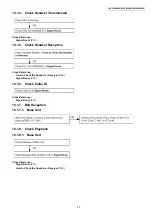
Page 39: ...5 Check Handset Reception Cross Reference How to Check the Speaker or Receiver P 55 Signal Route P 15 10 1 6 Check Caller ID Cross Reference Signal Route P 15 10 1 7 Bell Reception 10 1 7 1 Base Unit 10 1 8 Check Playback 10 1 8 1 Base Unit Cross Reference Signal Route P 15 How to Check the Speaker or Receiver P 55 ...

Page 40: ...n you can confirm the current frequency of CLK 2 Adjust the frequency of CLK executing the command setfreq xx where xx is the value so that the reading of the frequency counter is 10 368000 MHz 10 Hz IC1 X1 R40 C44 C45 E DTMF Generator Check 1 Connect CN101 Telephone Socket to DTMF tester Road 600 Ω 2 Link Handset and push dial key 3 Confirm DTMF character 4 Confirm that the high Group is 7dBm 3dB...

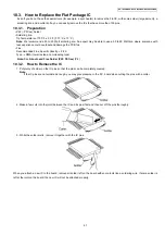
Page 41: ...amage the PCB foil Flux Recommended Flux Specific Gravity 0 82 Type RMA lower residue non cleaning type Note See About Lead Free Solder Pbf Pb free P 4 10 3 2 How to Remove the IC 1 Put plenty of solder on the IC pins so that the pins can be completely covered Note If the IC pins are not soldered enough you may give pressure to the P C board when cutting the pins with a cutter 2 Make a few cuts in...

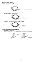
Page 42: ...acy of the IC setting with the corresponding soldering foil 2 Apply flux to all pins of the FLAT PACKAGE IC 3 Solder the pins sliding the soldering iron in the direction of the arrow 10 3 4 How to Remove a Solder Bridge 1 Lightly resolder the bridged portion 2 Remove the remaining solder along the pins using a soldering iron as shown in the figure below ...

Page 43: ...43 KX TG2853BXS KX TG2854BXS KX TGA280BXS 11 Disassembly and Assembly Instructions 11 1 Disassembly Instructions 11 1 1 Base Unit ...

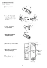
Page 44: ...44 KX TG2853BXS KX TG2854BXS KX TGA280BXS 11 1 2 Handset ...

Page 45: ...45 KX TG2853BXS KX TG2854BXS KX TGA280BXS 11 1 3 Charger Unit ...

Page 46: ...46 KX TG2853BXS KX TG2854BXS KX TGA280BXS 11 2 Fix the LCD to the Main P C Board Handset ...

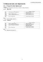
Page 47: ...1 BandGAP adjustment 2 Standard frequency adjustment Flash ROM IC501 Memory of software program Memory of Adjustment parameter data 1 BandGAP adjustment 2 Standard frequency adjustment Xtal X1 Source of system clock 1 Standard frequency adjustment IC Necessary Adjustment BBIC IC1 Memory of software program CPU interface for RF and FlashROM 1 BandGAP adjustment 2 Standard frequency adjustment EEP R...

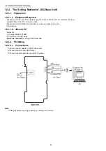
Page 48: ...A is recommended Digital multi meter DMM It must be able to measure voltage and current Oscilloscope 12 2 1 2 JIG and PC Serial JIG JIG Cable PQZZ1CD300E PC which runs in DOS mode Batch file CD ROM for setting PQZZTG2873BX 12 2 2 PC Setting 12 2 2 1 Connections Connect the AC adaptor to CN301 base unit Connect the JIG Cable GND black Connect the JIG Cable RX red and TX yellow Note COM port names m...

Page 49: ...49 KX TG2853BXS KX TG2854BXS KX TGA280BXS 12 2 2 2 Batch file Settings Note varies depending on the country Refer to Commands P 51 for frequently used commands ...

Page 50: ...o measure voltage and current Oscilloscope 12 3 1 2 JIG and PC Serial JIG JIG Cable PQZZ1CD300E PC which runs in DOS mode Batch file CD ROM for setting PQZZTG2873BX Note If you have the JIG Cable for TCD500 series PQZZ1CD505E change the following values of resis tance 12 3 2 PC Setting 12 3 2 1 Connections Connect the DC Power or Battery to CHG and CHG handset Connect the JIG cable GND black Conne...

Page 51: ...value Type bandgap then registered bandgap adjust value is read out bandgap nn Set VDD voltage adjustment parameter value Type bandgap nn nn is an adjustment setting value of the bandgap voltage conttx Set RFC burst mode Type conttx then set RF burst mode setfreq Check frequency adjustment parameter value Type setfreq then registered freq adjustment value is read out setfreq nn Set frequency adjus...

Page 52: ...52 KX TG2853BXS KX TG2854BXS KX TGA280BXS 12 5 Adjustment of Handset Cross Reference Power Supply Circuit P 12 ...

Page 53: ...F Tester Call ID Simulator BELL Simulator LOOP Simulator AF OSC AF VOLT METER OSC 600 Ω 12 Ω 2W CHARGE CHARGE Digital Volt Meter DCP GND DC POWER 7 0 V Frequency Counter U ART PC GND CLK 10 368MHz Digital Volt Meter LINE_DC GND VDD2 Digital Volt Meter VDD1 VDD3 SP SP PQUP11400Z PbF SV06 TG2851 TG2853 LINE_DC L1T L1R RST CLK ANT_1 ANT_2 VDD3 DCP CHG WHT RED DCM 2 2 1 1 VDD2 YELLOW SP GNDUTX URX A V...

Page 54: ...70 Q301 Q302 URX UTX GND R103 R102 C504 R504 L502 Q502 R502 Q500 R500 R503 C422 D401 D400 R74 R3 C4 C503 R85 C2 80 1 C61 C60 C6 X1 R5 R60 IC1 R505 R506 C5 C306 R414 R4 L2 C421 R408 R409 L503 R100 R101 Q100 C420 R405 R402 R80 C1 R82 C3 R2 R89 L1 R83 DG R81 C400 C405 R401 C403 C407 C8 R6 C14 R415 R400 2 5V R75 R71 C71 R70 JTAG Q500 C417 C502 CHG C501 C505 R501 C500 D501 CHG VBAT D1 C304 IC301 C300 C...

Page 55: ... TG2853BXS KX TG2854BXS KX TGA280BXS 12 8 How to Check the Speaker or Receiver 1 Prepare the digital voltmeter and set the selector knob to ohm meter 2 Put the probes at the speaker terminals as shown below ...

Page 56: ...37 2433 8880 38 2434 7520 39 2435 6160 40 2436 4800 41 2437 3440 42 2438 2080 43 2439 0720 44 2439 9360 45 2440 8000 46 2441 6640 47 2442 5280 48 2443 3920 49 2444 2560 50 2445 1200 51 2445 9840 52 2446 8480 53 2447 7120 54 2448 5760 55 2449 4400 56 2450 3040 57 2451 1680 58 2452 0320 59 2452 8960 60 2453 7600 61 2454 6240 62 2455 4880 63 2456 3520 64 2457 2160 65 2458 0800 66 2458 9440 67 2459 80...

Page 57: ...57 KX TG2853BXS KX TG2854BXS KX TGA280BXS Memo ...

Page 58: ...he development of new technology 13 1 2 Handset Schematic Diagram Handset Notes 1 DC voltage measurements are taken with an oscilloscope or a tester with a ground 2 The schematic diagram may be modified at any time with the development of new technology 13 1 3 Charger Unit Schematic Diagram Charger Unit Notes 1 DC voltage measurements are taken with voltmeter from the negative voltage line 2 The s...

Page 59: ...PD7 11 P3 1 PD1 12 P3 5 PD5 13 P3 4 PD4 14 P3 3 PD3 15 P3 2 PD2 16 VDD 16 17 VSS 17 18 RFCLK 19 VDDRF 20 VSSRF 21 XTAL1 22 CAP 23 AVS 24 AVD 25 RSSI 26 RDI 27 CMPREF 28 TDO 29 AD15 30 AD16 31 AD17 32 AD18 33 AD19 34 AD20 35 AD21 36 AD22 37 AD23 38 LE 39 SO 40 SK 41 DAC ADC2 42 P3 6 PD6 43 RDN 44 WRN 45 MI READY 46 SCLK 47 UTX P0 0 48 URX P0 1 49 JTIO P0 2 50 PCM_FSC1 P0 3 51 PCM_FSC0 P0 4 52 PCM_C...

Page 60: ...1K R775 1K R748 0 100K R185 R779 100K R777 0 R93 10K R737 0 R95 1K R96 1K D183 GND1 GND R719 330 R718 330 150K R186 C740 C5p C741 C5p C744 C3p R753 47K 1005 C765 J15p R752 6 8K L705 0 56uH 220 R743 C783 J15p SPM SPP C753 J390p 1 GND1 2 GND2 3 GND3 4 TXDATA 5 RSSI 6 VCC_OC 7 GND4 8 SYCL 9 SYDA 10 SYEN RXDSG 12 11 SYRI 13 GND5 14 GND6 15 GND7 16 GND8 17 GND9 18 GND10 19 RXDA 20 GND11 21 GND12 22 PSE...

Page 61: ...3 Schematic Diagram Base Unit_Operation Vol up LED1 ANSWER STOP Vol down INT ERASE REPEAT LED2 CN1 1 NC 2 ROW0 3 ROW1 4 ROW2 5 COL0 6 COL1 7 COL2 8 LED2 9 LED1 10 VDD IN USE ANS NC No Components KX TG2853 2854 SCHEMATIC DIAGRAM Base Unit_Operation ...

Page 62: ...62 KX TG2853BXS KX TG2854BXS KX TGA280BXS Memo ...

Page 63: ...72 MICp 73 VREFp 74 P3 0 75 P1 4 INT4n 76 P1 3 INT3n 77 P2 2 CLK100 78 AVS_sense 79 ADC3 80 ADC0 C11 K1u K0 01u C8 C400 NC K0 01u C1 K0 01u C2 R7 NC C403 NC LED1 VBAT LED6 LED5 LED7 LED8 DG DG DG DG DG DG DG DG DG DG DG DG DG C301 NC R2 100 DG DG DG DG C202 NC CA200 NC 1 2 3 4 5 6 7 8 2 5V DG DG C201 NC C203 NC L1 68n C504 NC DG AG RFG R5 270 PCM DO DG PCM FO PCM CK R300 0 1 1 8W Q300 C200 NC C4 K...

Page 64: ...RCV1 RCV1 SP1 SP2 C405 K0 1u C407 K0 1u C714 J270p D400 3 3V D401 3 3V DG C423 NC DG C424 NC D402 3 3V D403 3 3V VDD5 K1u C307 K1u C308 IC300 1 VOUT 2 GND 3 VDD 4 CE 5 NC DG C451 NC C450 NC C466 NC L400 L401 C302 6 3V330u C303 6 3V330u L450 10uH L451 10uH R412 220 R413 220 IC2 64K 1 A0 2 A1 3 A2 4 GND 5 SDA 6 SCL 7 WP 8 VCC B2 4p C712 C715 NC C716 NC RFG RFG C422 K0 01u C421 NC AG R713 1 2K C415 K...

Page 65: ...853BXS KX TG2854BXS KX TGA280BXS 13 5 Schematic Diagram Charger Unit 68 1 2W R4 68 1 2W R3 68 1 2W R2 68 1 2W R1 CN1 1 2 TP1 TP2 DC IN 6 5V For Charger Terminal Land for soldering SCHEMATIC DIAGRAM Charger Unit ...

Page 66: ...15 C7 IC301 R304 R305 R306 C306 D308 R310 R309 R308 C312 C310 R775 C778 R780 R778 C763 R777 R779 C767 C770 R737 C732 R719 C742 L703 C744 C741 C740 DA701 C771 C783 IC701 L704 C755 C768 R767 C774 C775 32 1 10 27 26 17 16 11 C749 R756 C773 R763 R736 C766 R748 R753 R752 C765 C733 R718 C743 R760 C753 L705 R743 C301 C302 R303 R302 C13 C20 C10 IC1 R9 J5 J6 R5 Q2 Q3 C332 C321 C320 C331 C333 R333 R334 R500...

Page 67: ...4 1 2 Flow Solder Side View PQUP11400Z PbF SV06 TG2851 TG2853 KX TG2853 2854 CIRCUIT BOARD Base Unit_Main Flow Solder Side View LINE_DC L1T L1R RST CLK ANT_1 ANT_2 VDD3 DCP CHG WHT RED DCM 2 2 1 1 VDD2 YELLOW SP GNDUTX URX VDD1 A CLK 10 368 MHz ...

Page 68: ...TG2854BXS KX TGA280BXS 14 2 Circuit Board Base Unit_Operation 14 2 1 Component View PQUP11401Z A PbF LED2 INT ERASE REAPET ANSWER UP STOP DOWN LED1 1 CN1 10 KX TG2853 2854 CIRCUIT BOARD Base Unit_Operation Component View ...

Page 69: ...69 KX TG2853BXS KX TG2854BXS KX TGA280BXS 14 2 2 Flow Solder Side View KX TG2853 2854 CIRCUIT BOARD Base Unit_Operation Flow Solder Side View PbF 1 2 4 3 5 PQUP11401Z A ...

Page 70: ...R85 C2 80 1 C61 C60 C6 X1 R5 R60 IC1 R505 R506 C5 C306 R414 R4 L2 C421 R408 R409 L503 R100 R101 Q100 C420 R405 R402 R80 C1 R82 C3 R2 R89 L1 R83 DG R81 C400 C405 R401 C403 C407 C8 R6 C14 R415 R400 2 5V R75 R71 C71 R70 JTAG Q500 C417 C502 CHG C501 C505 R501 C500 D501 CHG VBAT D1 C304 IC301 C300 C303 C302 R706 C704 R704 C705 C710 C715 R413 D403 C424 C419 C711 R713 R716 C423 ANT_1 ANT_2 C418 D402 PbF ...

Page 71: ...0 R208 R205 R207 R206 LED2 Func2 VOICE Func1 EXT SP 1 2 3 4 5 6 7 Catch INT MIC 8 9 0 HOLD OFF UP DOWN LED5 LED6 LED7 LED8 RIGHT LEFT LED3 LED4 R200 LED1 PbF PFUP1609Z A MIC MIC 22 1 CN200 Func2 VOICE Func1 EXT SP 1 2 3 4 5 6 7 Catch INT MIC 8 9 0 HOLD OFF UP DOWN RIGHT LEFT PbF PFUP1609Z A PCB CH REF CH AUTO CH KX TGA280 CIRCUIT BOARD Handset Flow Solder Side View ...

Page 72: ...72 KX TG2853BXS KX TG2854BXS KX TGA280BXS 14 4 Circuit Board Charger Unit 14 4 1 Component View R1 R4 PbF PFUP1569Z A R2 CIRCUIT BOARD Charger Unit Component View R3 BX CN CN1 1 2 ...

Page 73: ... Non use D O H 47 UART TX_DATA D O RUN BOOT I PU 48 UART RX_DATA D I I PD 49 JTAG DATA i f D I Debug MODE I PU 50 key Scan D I Non Key in I PU 51 key Scan D I Non Key in I PU 52 key Scan D I Non Key in I PU 53 Non use 54 SP AMP_CD D O ON OFF 55 Digital Source 3 0V VDD 56 Digital GND DGN D 57 ANS LED D O ON OFF 58 INUSE_LED D O ON OFF 59 key Scan D O Non Key in I PU 60 ROM_CS D O CS on H 61 key Sca...

Page 74: ...alog O 113 CID AMPO A O Analog Analog O 114 CID Signal INPUT A I Analog Analog I 115 AFE GND GND O 116 MIC Bias A O O 117 Analog REF 0 9V A O O 118 LINE IN A I Analog Analog I 119 Non use A O I PU 120 Ext Reset IN I 1 8 V Reset I PU 121 ROM Select D I External Internal I 122 Address bus D O H 123 Address bus D O H 124 Address bus D O H 125 Address bus D O H 126 Address bus D O H 127 Address bus D ...

Page 75: ...2 5 V 39 Digital Source 1 8V 1 8 V 40 Key Scan D I Non key in I PU 41 Mode control UART TX data D O RST usually mode RST Boot mode I PU 42 UART RX data D I I PU 43 Modecontrol JTAG i f D I RST usually mode RST Debug mode I PU 44 EEPROM Serial Data D O I PU 45 EEPROM Serial Clock D O I PU 46 Key Scan D O Non key in I PU 47 Key Scan D O Non key in I PU 48 Key Scan D O Non key in I PU 49 Digital GND ...

Page 76: ... KX TG2853BXS KX TG2854BXS KX TGA280BXS Note The mark in the I O column means the port is controlled by the firmware 79 Charge current monitor A I A D A D I 80 NC A I I PIN Description I O High High_Z Low ...

Page 77: ...77 KX TG2853BXS KX TG2854BXS KX TGA280BXS 15 3 Terminal Guide of the ICs Transistors and Diodes 15 3 1 Base Unit 15 3 2 Handset ...

Page 78: ...78 KX TG2853BXS KX TG2854BXS KX TGA280BXS 16 Exploded View and Replacement Parts List 16 1 Cabinet and Electrical Parts Base Unit ...

Page 79: ...79 KX TG2853BXS KX TG2854BXS KX TGA280BXS 16 2 Cabinet and Electrical Parts Handset Note 1 Attach the spacer No 109 to the exact location described above ...

Page 80: ...80 KX TG2853BXS KX TG2854BXS KX TGA280BXS 16 3 Cabinet and Electrical Parts Charger Unit ...

Page 81: ...81 KX TG2853BXS KX TG2854BXS KX TGA280BXS 16 4 Accessories and Packing Materials 16 4 1 KX TG2853BXS ...

Page 82: ...82 KX TG2853BXS KX TG2854BXS KX TGA280BXS 16 4 2 KX TG2854BXS ...

Page 83: ...83 KX TG2853BXS KX TG2854BXS KX TGA280BXS 16 4 3 KX TG280BXS ...

Page 84: ...LDER CHARGETERMINAL R POM HB 8 PQKE10436Y1 CASE CHARGE TERMINAL PS HB 9 PQGG10410Z1 GRILLE CRADLE ABS HB 10 PQHR11082Z GUIDE SP HOLDER POM HB 11 L0AA04A00028 SPEAKER 12 PQJE10162X LEAD WIRE FFC 13 PQSX10316Z KEYBOARD SWITCH 14 PQBC10464Y1 BUTTON STOP ABS HB 15 PQHR11209Z GUIDE POM HB 16 PQBC10469Y2 BUTTON NAVIGATOR KEY ABS HB 17 PQBC10463Z1 BUTTON ANSWER ON ABS HB 18 PQHR11210Z OPTIC CONDUCTIVE PA...

Page 85: ...YJ103 10K R779 ERJ2GEJ104 100K Ref No Part No Part Name Description Remarks C181 ERJ6GEY0R00 0 J5 ERJ2GE0R00 0 J7 ERJ2GEJ103 10K CAPACITORS C7 ECUV1A224KBV 0 22 C9 ECJ0EB1C103K 0 01 C10 ECJ0EB1C103K 0 01 C12 ECJ0EB1C103K 0 01 C13 ECJ0EB1A104K 0 1 C17 ECJ0EB1C103K 0 01 C18 ECUV1A105KBV 1 C19 ECJ0EC1H100D 10P C20 ECJ0EC1H100D 10P C22 ECJ0EB1C103K 0 01 C24 ECJ0EB1C103K 0 01 C25 ECJ0EB1C103K 0 01 C27 ...

Page 86: ...BOARD SWITCH 123 PQBC10458Y2 BUTTON NAVIGATOR KEY ABS HB 124 PQHS10722Z SPACER LCD 125 PQKM10708V1 CABINET BODY ABS HB 126 PQHS10721Z TAPE DOUBLESIDED PANEL 127 PQGP10300T1 PANEL LCD AS HB 128 PQGT18977Z NAME PLATE Ref No Part No Part Name Description Remarks Ref No Part No Part Name Description Remarks PCB100 PFWPG2853BXR MAIN P C BOARD ASS Y RTL ICs IC1 PFWI12853BXR IC 1 IC2 PFWI22853BXR IC 1 IC...

Page 87: ...04 22 C305 ECUV1A105KBV 1 C306 ECUV1A105KBV 1 C307 ECUV1A105KBV 1 C308 ECUV1A105KBV 1 C309 PQCUV1A105KB 1 S C310 PQCUV1A105KB 1 S C405 ECUE1A104KBQ 0 1 S C407 ECUE1A104KBQ 0 1 S C415 ECUV1C104KBV 0 1 C417 ECJ0EC1H100D 10P C420 ECST0JY226 22 S C422 ECJ0EB1C103K 0 01 Ref No Part No Part Name Description Remarks C501 ECUV1C104KBV 0 1 C503 ECUV1A105KBV 1 C505 F1H1A105A036 1 C700 ECJ0EC1H100D 10P C701 ...

Page 88: ...RUCTION BOOK for English 1 A104 PQQX15155Z INSTRUCTION BOOK for Thai 1 A105 PQQW15151Z LEAFLET QUICK GUIDE for Arabic A106 PQQW15152Z LEAFLET QUICK GUIDE for Persian P101 XZB21X35A03 PROTECTION COVER for Base Unit P102 XZB10X35A02 PROTECTION COVER for Hand set P103 XZB15X25A04 PROTECTION COVER for Charger Unit P104 PQPK15380Z GIFT BOX Ref No Part No Part Name Description Remarks A201 PQLV207BXZ AC...

Reviews: