background image

16

KX-TG6071BXM/KX-TGA601BXM

4.5.5.

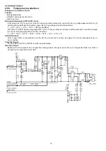
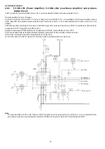
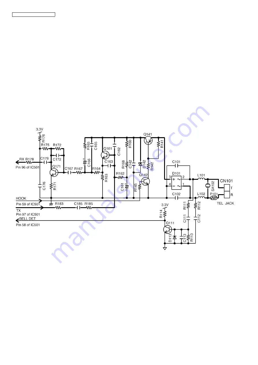
Telephone Line Interface

Telephone Line Interface Circuit:
Function

• Bell signal detection
• ON/OFF hook and pulse dial circuit
• Side tone circuit

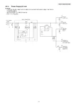
Bell signal detection and OFF HOOK circuit:

In the idle mode, Q141 is open to cut the DC loop current and decrease the ring load. When ring voltage appears at the Tip (T)
and Ring (R) leads (When the telephone rings), the AC ring voltage is transferred as follows:

 L101 

 R111 

 C111 

 Q111 

 DSP pin 58 [BELL]

When the CPU (DSP) detects a ring signal, Q141 turns on, thus providing an off-hook condition (active DC current flow through
the circuit). Following signal flow is the DC current flow.

 L101 

 D101 

 Q141 

 Q161 

 R163 

 D101 

 L102 

 P101 

 R

ON HOOK Circuit:

Q141 is open, Q141 is connected as to cut the DC loop current and to cut the voice signal. The unit is consequently in an on-
hook condition.

Pulse Dial Circuit:

Pin 59 of DSP turns Q141 ON/OFF to make the pulse dialing.

Side Tone Circuit:

Basically this circuit prevents the TX signal from feeding back to RX signal. As for this unit, TX signal feed back from Q161 is
canceled by the canceller circuit of DSP.

Summary of Contents for KX-TG6071BXM

Page 1: ...hts reserved Unauthorized copying and distribu tion is a violation of law ORDER NO KM40704321CE Telephone Equipment KX TG6071BXM KX TGA601BXM 5 8 GHz Digital Cordless Answering System Metallic Gray Version for Asia Middle Near East and Other areas ...

Page 2: ...2 KX TG6071BXM KX TGA601BXM ...

Page 3: ...e LLP Leadless Leadframe Package IC 68 11 Disassembly and Assembly Instructions 70 11 1 Disassembly Instructions 70 11 2 How to Replace the Handset LCD 73 11 3 Antenna Soldering Work 75 12 Measurements and Adjustments 76 12 1 Things to Do after Replacing IC or X tal 76 12 2 Base Unit Reference Drawing 77 12 3 Handset Reference Drawing 78 12 4 Frequency Table 79 13 Schematic Diagram 80 13 1 For Sch...

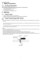
Page 4: ...andard solder or solder that con tains lead We will use PbF solder when discussing the lead free solder used in our manufacturing process which is made from Tin Sn Silver Ag and Copper Cu This model and others like it manufactured using lead free solder will have PbF stamped on the PCB For service and repair work we suggest using the same type of solder Caution PbF solder has a melting point that ...

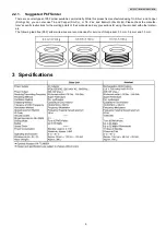
Page 5: ...per Sn Ag Cu you can also use Tin and Copper Sn Cu or Tin Zinc and Bismuth Sn Zn Bi Please check the manufac turer s specific instructions for the melting points of their products and any precautions for using their product with other materi als The following lead free PbF solder wire sizes are recommended for service of this product 0 3 mm 0 6 mm and 1 0 mm 3 Specifications ...

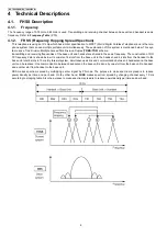
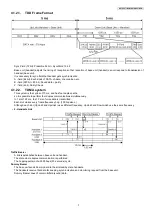
Page 6: ...ncies of the base unit and handset are shared in the same frequency The construction of RX TX frequency data is shown below It consists of 4 slots from the base unit to the handset and 4 slots from the handset to the base unit total 8 slots in 10 ms By this slot system simultaneous air link and communication between 4 handsets and the base unit can be realized One communication between handset and...

Page 7: ...x paths so it is possible to perform four duplex communications simultaneously In 1 slot 1 25 ms the 10 ms of voice data is transmitted Each slot makes every frame frequency hop 100 hops sec Although each slot UpLink3 and UpLink4 uses different frequency UpLink3 and DownLink3 use the same frequency 2 Handsets Link Traffic Bearer A link is established between base unit and handset The state where d...

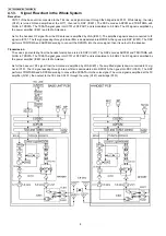
Page 8: ...then goes into DSP IC501 The DSP performs TDD TDMA and ADPCM decoding to convert the RXDATA into the voice signal then it is output to the speaker Transmission The voice signal entering from the handset microphone is led to DSP IC501 The DSP encodes ADPCM and TDD TDMA with FHSS to TXDATA The TXDATA signal goes into IC701 of RF PART and is modulated to 5 8 GHz The RF signal is amplified by the powe...

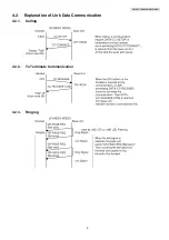
Page 9: ...9 KX TG6071BXM KX TGA601BXM 4 2 Explanation of Link Data Communication 4 2 1 Calling 4 2 2 To Terminate Communication 4 2 3 Ringing ...

Page 10: ...IN CID IN IC501 DSP 4 0 V CONVERTOR MIN INUSE DETECT 2 INUSE DETECT 1 RECEIVE AMP DCIN 1 DCIN 2 IC331 RESET POWER_DOWN VCCIN VCC VCCA VCCPA INT_1 CHARGE_DET V_RF INT_1 5 VCC ANSWER_LED SP_LED IC601 FLASH MEMORY KEYS IC300 Q300 R151 R152 R131 R133 Q171 BCLK RADIO_EN TX_EN RX_EN SLOT_CTRL SYN_DATA SYN_CLK TXDATA V_RF VPA SI SO CS IN USE_LED MSG_LED KEY1 6 KEYA E SPOUTP SPOUTN RXDATA MIP SYN_EN SYN_O...

Page 11: ...3 0 V REGULATOR IC761 PLL delta sigma Modulator IC701 Doubler 2x Control Logic Modem A D PAEN ANTSEL_A ANTSEL_B LNA_EN RXGAIN VCC_PLLA VCC_VCO VCC_PLLD VCC_PA VCC_FE VCC_IF VCC_DIG RADIO_EN KX TG6071 BLOCK DIAGRAM Base Unit_RF Part SLOT_CTRL SYN_DATA SYN_CLK SYN_EN SYN_OUT BCLK DSP IC501 V_RF V_PA IC801 FL711 FL721 IF 432 kHz FL811 FL821 ...

Page 12: ...s from the Flash Memory DTMF Generator When the DTMF data from the handset is received the DTMF signal is output Synthesized Voice Pre recorded message The DSP implements synthesized Voice utilizing the built in speech detector and a Flash Memory which stored the vocabulary Caller ID demodulation The DSP implements monitor and demodulate the FSK DTMF signals that provide CID information from the C...

Page 13: ... KX TGA601BXM 4 5 3 Power Supply Circuit Function The power supply voltage from AC adaptor is converted to the desired voltage of each block Circuit Operation Q300 and IC300 4 0 V DCDC Converter IC331 3 3 V Regulator ...

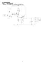
Page 14: ...14 KX TG6071BXM KX TGA601BXM 4 5 3 1 Charge Circuit The voltage from the AC adaptor is supplied to the charge circuits ...

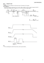
Page 15: ...rporates an AC adaptor Circuit Operation When the AC Adaptor is inserted into the unit then the voltage is shifted by IC331 and power is supplied to the DSP The set starts to operate when VCC goes up to 3 0 V or more in the circuit voltage diagram Note 1 The initializing time of the DSP chip is 28 ms under normal conditions ...

Page 16: ...DSP pin 58 BELL When the CPU DSP detects a ring signal Q141 turns on thus providing an off hook condition active DC current flow through the circuit Following signal flow is the DC current flow T L101 D101 Q141 Q161 R163 D101 L102 P101 R ON HOOK Circuit Q141 is open Q141 is connected as to cut the DC loop current and to cut the voice signal The unit is consequently in an on hook condition Pulse Di...

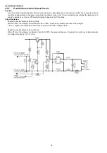
Page 17: ...ransmitting status Circuit Operation The voltage of pin 90 of IC501 is monitored If a parallel connected telephone is put into OFF HOOK status the presence absence of a parallel connection is determined when the voltage changes by 0 2 V or more When the set detects the parallel connected telephone is OFF HOOK status the line is disconnected You can enable or disable the Auto Disconnect function Se...

Page 18: ...ected in parallel is on hook or off hook by detecting changes in the T R voltage Circuit Operation Parallel connection detection when on hook When on hook the voltage is monitored at pin 86 of IC501 There is no parallel connection if the voltage is 1 65 V or higher while a parallel connection is deemed to exist if the voltage is lower Parallel connection detection when off hook When off hook the v...

Page 19: ...er method of FSK or DTMF The method is chosen according to the exchange of telephone office This unit is available to receive the data with both methods and displays the received data on LCD FSK Frequency Shift Keying format DTMF format It is the method to send the telephone number of calling party with DTMF to the telephone DTMF is sent before the first bell sig nal The data is sent in turn first...

Page 20: ...N_DATA SYN_CLK SYN_LE1 RX_GAIN RX_EN TX_EN SHCTRL RF_RESET RSSI WP CLK DATA KEYSTOROBE_A F KEYIN_1 5 Q531 CHARGE DETECT CHARGE Q361 D361 Q521 Q362 Q363 CHARGE CONTROL RESET POWER DOWN IC561 DC DC CONVERTER REGULATOR MIC SP Headset Jack CN431 Q431 LED561 HEADSET DETECT Monitor SP 3 3 V REGULATOR LCD KEYS RF part ANT X501 13 824 MHz EEPROM BATTERY PA_CONT TX_DATA RX_DATA OSC_IN Q561 Q555 LCD BACK LI...

Page 21: ...l Logic Modem A D KX TGA601 BLOCK DIAGRAM Handset_RF Part TXDATA RXDATA ANT1 ANT2 PLL delta sigma Modulator IC701 Doubler 2x PAEN ANTSEL_A ANTSEL_B LNA_EN RXGAIN VCC_PLLA VCC_VCO VCC_PLLD VCC_PA VCC_FE VCC_IF VCC_DIG RADIO_EN SLOT_CTRL SYN_DATA SYN_CLK SYN_EN SYN_OUT BCLK RF_POWER DSP IC501 V_RF V_PA IC801 FL711 FL721 IF 432 kHz FL811 FL821 ...

Page 22: ...ttery Low Power down detect circuit Ringer Generation Interface circuit RF part Speaker Mic LED Key scan LCD Headset Initial waves Note 1 The initializing time of the DSP chip is 20 ms under normal conditions 4 8 1 2 RF part Mainly voice signal is modulated to RF or it goes the other way 4 8 1 3 EEPROM IC541 All setting data is stored ex ID code user setting Phonebook Caller ID data ...

Page 23: ...23 KX TG6071BXM KX TGA601BXM 4 8 2 Power Supply Circuit Voltage is supplied separately to each block ...

Page 24: ...The voltage between CHARGE and CHARGE flows R531 Q531 pin 38 of IC501 where the charge is detected Then IC501 calculates the battery consumption amount from the previous charge and it controls Q361 Q362 Q363 by pin 80 of IC501 until charging is complete When charging is complete the control pattern is switched to Trickle charging form from Operational charging form 4 8 4 Ringer and Handset SP Phon...

Page 25: ...set is input to DSP 95 Also the power for the microphone is supplied from DSP 92 and the power is turned OFF on standby 4 8 6 Reception Signal The voice signal from the base unit is output to DSP 98 This signal is led to the headset jack CN431 The signal through the headset jack and the other signal output from DSP 97 drives the speaker When the headset is inserted to the jack the voice signal is ...

Page 26: ...ansmitted On the other hand received signals are demodulated and go out to DSP 4 9 1 Power Supply Circuit As indicated below the various voltages are supplied to each block V_PA about 4 0 V at base unit or 3 3 V at handset is supplied to the Power amplifier in 5 8 GHz PA circuit IC761 is 3 0 V Regulator and outputs VRF 3 0 V by order of RADIO_EN signal V_RF is approximately 4 0 V Base Unit or 3 6 ...

Page 27: ...ugh BALUN BALunce UNbalunce matching cir cuit and supplied to pin 7 and pin 8 In IC701 RX signal is down converted to 432 kHz IF signal and demodulated and RX digital data RX_DATA goes from pin 17 to DSP IC701 outputs some digital signals PAEN ANTSEL_A ANTSEL_B LNAEN RXGAIN and controls IC801 Reference Clock signal 13 824 MHz is supplied to pin 25 Note The exposed GND_PLATE on the bottom of the IC...

Page 28: ...ies receiving 5 8 GHz signal 5 8 GHz RX signal from Antenna Switch block of IC801 is amplified by LNA block and is supplied to IC701 through 5 8 GHz BPF FL721 Antenna Switch block of IC801 switches for RF signals by ANTSEL_A and ANTSEL_B from IC701 IC701 checks RSSI Received Signal Strength Indicator and selects better receiving condition antenna At RX mode RX signal is lead from selected antenna ...

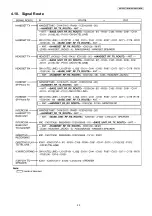
Page 29: ...29 KX TG6071BXM KX TGA601BXM 4 10 Signal Route ...

Page 30: ...30 KX TG6071BXM KX TGA601BXM RF part signal route ...

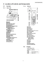
Page 31: ...31 KX TG6071BXM KX TGA601BXM 5 Location of Controls and Components 5 1 Controls 5 1 1 Base Unit 5 1 2 Handset 5 2 Display ...

Page 32: ...32 KX TG6071BXM KX TGA601BXM 6 Installation Instructions 6 1 Setting Up the Base Unit 6 1 1 Connecting the AC Adaptor and Telephone Line Cord 6 2 Battery Installation Replacement ...

Page 33: ...h may not be indicated correctly if the battery is disconnected and connected again even after it is fully charged In that case by recharging the battery as mentioned above you will get a correct indication of the battery strength 6 3 1 Battery Level 6 3 2 Panasonic Battery Performance ...

Page 34: ...34 KX TG6071BXM KX TGA601BXM 7 Operation Instructions 7 1 Programmable Settings 7 1 1 Programming by Scrolling through the Display Menus ...

Page 35: ...35 KX TG6071BXM KX TGA601BXM 7 1 2 Programming using the Direct Commands ...

Page 36: ...36 KX TG6071BXM KX TGA601BXM 7 2 Dial Lock For Service Hint If the current password is forgotten refer to Dial lock in Troubleshooting P 38 ...

Page 37: ...37 KX TG6071BXM KX TGA601BXM 7 3 Error Messages ...

Page 38: ...38 KX TG6071BXM KX TGA601BXM 7 4 Troubleshooting ...

Page 39: ...39 KX TG6071BXM KX TGA601BXM ...

Page 40: ...40 KX TG6071BXM KX TGA601BXM ...

Page 41: ...41 KX TG6071BXM KX TGA601BXM 8 Test Mode 8 1 Adjustment and Test Mode Flow Chart 8 1 1 Test Burst Mode for Base Unit Note 1 Refer to Check Table for RF part P 60 ...

Page 42: ...42 KX TG6071BXM KX TGA601BXM 8 1 2 TX CW Mode for Base Unit Note 1 Refer to Check Table for RF part P 60 ...

Page 43: ...43 KX TG6071BXM KX TGA601BXM 8 1 3 RX CW Test Mode for Base Unit Note 1 Refer to Check Table for RF part P 60 ...

Page 44: ...1BXM 8 1 4 Test Link Mode for Base Unit Note 1 Refer to Test Link Mode for Handset P 49 If you can not proceed to the next step refer to Registering a Handset P 58 2 Refer to Check Table for RF part P 60 3 For factory use only ...

Page 45: ...45 KX TG6071BXM KX TGA601BXM 8 1 5 Adjustment Mode for Base Unit Cross Reference Check and Adjust Frequency Base Unit P 76 ...

Page 46: ...46 KX TG6071BXM KX TGA601BXM 8 1 6 Test Burst Mode for Handset Note 1 LCD displays the Channel number exception default CH00 1ch 2 Refer to Check Table for RF part P 60 ...

Page 47: ...47 KX TG6071BXM KX TGA601BXM 8 1 7 TX CW Mode for Handset Note 1 LCD displays the Channel number exception default CH00 1ch 2 Refer to Check Table for RF part P 60 ...

Page 48: ...48 KX TG6071BXM KX TGA601BXM 8 1 8 RX CW Test Mode for Handset Note 1 LCD displays the Channel number exception default CH00 1ch 2 Refer to Check Table for RF part P 60 ...

Page 49: ...1 9 Test Link Mode for Handset Note 1 LCD displays the Channel number exception default CH00 1ch 2 If can not proceed to the next step refer to Registering a Handset P 58 3 for factory use only 4 Refer to Check Table for RF part P 60 ...

Page 50: ... KX TGA601BXM 8 1 10 Adjustment Mode for Handset Cross Reference 1 Adjust Battery Low Detector Voltage Handset P 76 Note 2 These are the default values 3 These values may not be fixed depending on the battery strength ...

Page 51: ...ear User Setting Units are reset to the Factory settings by this operation Erase recorded Voice messages stored Phone numbers Caller list and etc This operation should not be performed for a usual repair 9 1 1 Base Unit Note 1 Telephone line must be connected ...

Page 52: ...52 KX TG6071BXM KX TGA601BXM 9 1 2 Handset Note 1 Be sure to short the battery terminals of the handset with a lead wire etc for 2 seconds for discharge after removing the battery ...

Page 53: ...RF part P 58 Check Handset Transmission P 65 Check Handset Reception P 65 Check Caller ID P 65 Check Sp phone Transmission P 56 Check Sp phone Reception P 56 Note 1 When a user claims that the unit disconnects a call right after the greeting message and no incoming messages can be recorded this symptom can not be reappeared with TEL simulator in the service center In this case try Check Record P 5...

Page 54: ...Check Power Cross Reference Power Supply Circuit P 13 Reset Circuit P 15 Note Flash Memory is IC601 DSP is IC501 1 Refer to Specifications P 5 for part number and sup ply voltage of AC adaptor 2 Refer to Circuit Board Base Unit_Main P 93 ...

Page 55: ...nnected telephone is OFF HOOK the line isn t disconnected D How to change the VOX level It makes easier to detect a small voice caller by raising the sensitivity of VOX level Therefore the recording of TAM is not turned off during a detection Cross Reference Signal Route P 29 Telephone Line Interface P 16 Auto Disconnect Circuit P 17 Parallel Connection Detect Circuit P 18 Note Flash Memory is IC6...

Page 56: ...s IC501 1 Refer to Circuit Board Base Unit_Main P 93 10 1 4 Check Sp phone Transmission Cross Reference Signal Route P 29 Telephone Line Interface P 16 Note Flash Memory is IC601 DSP is IC501 10 1 5 Check Sp phone Reception Cross Reference Telephone Line Interface P 16 Signal Route P 29 Note Flash Memory is IC601 DSP is IC501 ...

Page 57: ...arge Note Flash Memory is IC601 1 Refer to Specifications P 5 for part number and supply voltage of AC adaptor 10 1 7 Check Link Note Flash Memory is IC601 DSP is IC501 1 Refer to Finding out the Defective part P 58 Cross Reference Check the RF part P 58 ...

Page 58: ... Re register the checked handset to the checked base unit and Regular HS to Regular BU Note 1 HS Handset 2 BU Base Unit 10 1 8 1 1 Registering a Handset Refer to Registration in Troubleshooting P 38 10 1 8 1 2 Deregistering a Handset Refer to Registration in Troubleshooting P 38 10 1 8 1 3 Deregistering All Handsets by the Base Unit ...

Page 59: ...XM KX TGA601BXM 10 1 8 2 RF Check Flowchart Each item 1 6 of RF Check Flowchart corresponds to Check Table for RF part P 60 Please refer to the each item Note 1 Refer to Things to Do after Replacing IC or X tal P 76 ...

Page 60: ...Frequency 13 824000 MHz 100 Hz 4 TX confirmation Regular HS BU Mode Test Burst Mode 4 HS BU to be checked Mode TX_CW Mode 1 1 Place the Regular HS about 15 cm away from the BU 2 Confirm RXDATA waveform of the Regu lar HS by Oscilloscope 5 8 1 Place the HS about 15 cm away from the Regular BU 2 Confirm RXDATA waveform of the Regu lar BU by Oscilloscope 6 8 5 RX confirmation Regular HS BU Mode TX_CW...

Page 61: ...en HS and BU Link OK TX Power of the HS is OK No Link TX Power of the HS is NG Range Confirmation RX TEST RX sensitivity check HS BU Mode Test Link Mode 1 1 Register Regular HS to BU to be checked 2 Set BU to Test Link mode 3 Set Regular HS to Test Link mode Set TX Power and RX Sensitivity of the BU and Regular HS by CHART1 At distance of about 5 m between HS and BU Link OK RX Sensitivity of the B...

Page 62: ...62 KX TG6071BXM KX TGA601BXM 10 1 8 5 RF DSP Interface Signal Wave Form Test Burst Mode ...

Page 63: ...63 KX TG6071BXM KX TGA601BXM Test Burst Mode ...

Page 64: ...64 KX TG6071BXM KX TGA601BXM Test Burst Mode and TX CW Mode when TX confirmation and RX confirmation ...

Page 65: ...When checking the RF part Refer to Check the RF part P 58 10 1 11 Check Caller ID Cross Reference Telephone Line Interface P 16 Calling Line Identification Caller ID P 19 Note Make sure the format of the Caller ID service of the Tele phone company that the customer subscribes to It is also recommended to confirm that the customer is really a subscriber of the service ...

Page 66: ...bout Lead Free Solder PbF Pb free P 4 10 2 2 How to Remove the IC 1 Put plenty of solder on the IC pins so that the pins can be completely covered Note If the IC pins are not soldered enough you may give pressure to the P C board when cutting the pins with a cutter 2 Make a few cuts into the joint between the IC and its pins first and then cut off the pins thoroughly 3 While the solder melts remov...

Page 67: ... the IC setting with the corresponding soldering foil 2 Apply flux to all pins of the FLAT PACKAGE IC 3 Solder the pins sliding the soldering iron in the direction of the arrow 10 2 4 How to Remove a Solder Bridge 1 Lightly resolder the bridged portion 2 Remove the remaining solder along the pins using a soldering iron as shown in the figure below ...

Page 68: ... efficiently choose the right sized nozzle of the hot air desoldering tool that matches the IC package Be careful about the temperature of the hot air desoldering tool not to damage the PCB and or IC 10 3 3 How to Remove the IC 1 Heat the IC with a hot air desoldering tool through the P C Board 2 Pick up the IC with tweezers etc when the solder is melted completely Note Be careful not to touch the...

Page 69: ...IC the positioning should be done very carefully 3 Heat the IC with a hot air desoldering tool through the P C Board until the solder on IC bottom is melted Note Be sure to place it precisely controlling the air volume of the hot air desoldering tool 4 After soldering confirm there are no short and open circuits with visual inspection 10 3 5 How to Remove a Solder Bridge When a Solder Bridge is fo...

Page 70: ...70 KX TG6071BXM KX TGA601BXM 11 Disassembly and Assembly Instructions 11 1 Disassembly Instructions 11 1 1 Base Unit ...

Page 71: ...71 KX TG6071BXM KX TGA601BXM ...

Page 72: ...72 KX TG6071BXM KX TGA601BXM 11 1 2 Handset ...

Page 73: ...73 KX TG6071BXM KX TGA601BXM 11 2 How to Replace the Handset LCD ...

Page 74: ...74 KX TG6071BXM KX TGA601BXM ...

Page 75: ... We recommend a 30 to 40 Watt soldering iron Solder the antenna P C board as below Solder the antenna P C board enough to cover copper area 6 points Be careful not to short out NG Condition View A Antenna P C board Antenna P C board Main P C board Main P C board When attaching the antenna P C board solder it vertically to the main P C board View A ...

Page 76: ...tolelance 30 Hz by pressing or key Adjustment Tolerance 13 824 MHz 30 Hz 5 Press TALK key to write the new frequency factor in EEPROM 6 Turn the power off Then this value is available Cross Reference Adjustment Mode for Handset P 50 12 1 4 Adjust Battery Low Detector Voltage Handset After handset s DSP IC501 or EEPROM IC541 replacement Re writing Battery Low voltage to EEPROM is required With foll...

Page 77: ... R111 R112 R122 R151 R308 R121 R361 R365 R364 C361 L501 L300 D472 D473 L101 L102 L472 L473 TG6051 31 WBX02 WBX01 TG6071 D300 D133 D153 JOINT2 CN301 ANT1 CN101 LED677 ANT2 IC300 IC331 IC501 IC601 Q340 Q111 Q171 SPN SPP2 NC1 SPP TXO RX1 RX2 INT0 RA501 URX2 UVCC VCC MIP MIN UTX2 UGND INT1 JO JC DVCC JI JS JG RST 1 4 8 5 Q300 CHARGE CHARGE Q361 Q362 C821 C822 C811 C726 C879 C876 C877 C764 1 1 8 24 17 ...

Page 78: ...4 C745 C573 CA574 CA571 C511 R531 Q531 R534 R532 R362 R361 R363 R354 R379 R370 MICP MICM R377 R376 BATTP BATTM CHG2 CHG1 R543 R542 R541 R505 R506 R507 R509 R378 R366 R528 R522 R523 R433 C433 R508 R434 R417 PDN VSS1 RX VSS2 VBAT1 TX TDO TDI TMS TCK VBAT2 R526 R524 R525 R510 R501 BCLK X501 R547 R431 R432 TX_EN RXI CI R435 R552 R551 C552 R554 C554 R553 C553 C563 C565 C562 R564 R561 R546 R560 C564 R56...

Page 79: ...1 12 0C 5769 513 44 2C 5798 053 76 4C 5826 593 13 0D 5770 405 45 2D 5798 945 77 4D 5827 485 14 0E 5771 297 46 2E 5799 837 78 4E 5828 376 15 0F 5772 189 47 2F 5800 728 79 4F 5829 268 16 10 5773 080 48 30 5801 620 80 50 5830 160 17 11 5773 972 49 31 5802 512 81 51 5831 052 18 12 5774 864 50 32 5803 404 82 52 5831 944 19 13 5775 756 51 33 5804 296 83 53 5832 836 20 14 5776 648 52 34 5805 188 84 54 58...

Page 80: ...urements are taken with voltmeter from the negative voltage line 2 The schematic diagrams may be modified at any time with the development of new technology 13 1 2 Handset Schematic Diagram Handset_Main Notes 1 DC voltage measurements are taken with an oscilloscope or a tester with a ground 2 The schematic diagrams may be modified at any time with the development of new technology ...

Page 81: ...81 KX TG6071BXM KX TGA601BXM Memo ...

Page 82: ...5 PDN 86 DCIN1 87 VREF 88 MIP 89 MIN 90 91 NC 92 GNDA 93 CID_IN 94 CID_IN 95 VCCA 96 LIN0 97 LOUT0 1 GNDPA 2 SPP 3 BMCCLK 23 RF_RSTN 24 RADIO_EN 25 NC 26 GND 27 VCC 28 SYN_EN 48 INT0 49 FLASH_SCK 50 NC 51 KEYS_E 52 KEYS_D 53 KEYS_C 73 CHARGE_DET 74 NC 75 INUSE_LED 76 ANS_LED 77 INT1 78 BANK2 98 NC 99 VCCPA 100 SPN D473 5 1V A K D472 5 1V A K 100n C531 100n C347 100 R176 K0 012 C457 K0 012 C458 2 7...

Page 83: ...22 K680P 50V C121 NC C184 C185 K0 018 NC C174 D101 4 3 1 2 1M R133 10M R151 3 9M R152 K0 01 C152 NC R132 NC R153 560 R165 D361 22V A K 1u C342 CN301 2 1 1 NC1 2 RESET 3 VDET 4 VIN 5 VOUT 6 NC2 7 GND 8 CD CN101 TEL JACK 1 2 K0 47 C331 22 R171 4 7k R142 3216 NC R169 NC C168 SA103 SA102 SA101 NC 2 1 35 47u C300 16 10u C166 25 10u Q141 B C E Q142 B C E Q156 NC B C E Q161 B C E Q111 B C E Q171 B C E Q3...

Page 84: ...811 C1P C821 C1P C713 0 R845 ANT1 ANT2 B0 1P C871 B0 2P C725 NC C873 C4p C843 C4p C844 0 R846 10p C876 C1p C721 B0 2p C724 3 3nH L724 C2p C726 0 R847 B0 2p C727 1 GND_ISO_1 2 ANT1 7 VDD_LNA1 3 GND_ISO_2 4 GND_ISO_3 5 ANT2 6 GND_ISO_4 8 GND_ISO_5 9 VDD_LNA2 10 GND_ISO_6 11 GND_ISO_7 12 LNA_OUT 13 LNA_GAIN 14 LNA_EN 15 ANTSEL_B 16 ANTSEL_A 17 PA_EN 18 PA_IN 25 PGND 24 TRSW_IN 23 GND_ISO_10 22 GND_IS...

Page 85: ...68 1 VIN 2 VSS 3 CE 5 VOUT 4 NC RF_RSTN NC C715 NC L761 K1 0 C766 390 R740 390 R741 220 R742 390 R743 1k R744 1k R745 NC R747 NC R749 NC R748 K1u C712 K1u C734 1 TX 2 PAEN 9 VCC_FE 3 ANTSEL_A 4 ANTSEL_B 5 LNAEN 6 RXGAIN 7 RXp 8 RXn 10 VCC_IF 11 VDD_IF 12 TEST_DIG 13 RST 14 GND_DIG 15 VDD_DIG 16 VCC_DIG 17 TR_DATA 18 RADIO_EN 19 SLOT_CTRL 20 SYN_DATA 21 SYN_CLK 22 SYN_EN 23 SYN_OUT 24 DTEST 25 REFI...

Page 86: ... MUTE 1 2 4 1 2 SHA 1 2 KEYS_E KEYIN6 KEYIN5 KEYIN4 SP_LED INUSE_LED ANS_LED MEG_LED 2APVCC KEYIN3 KEYIN1 KEYS_C KEYS_B KEYIN2 KEYS_A KEYS_D SKIP 1 2 ANS 1 2 STOP 1 2 MSG VM 1 2 SPP2 DOWN 1 2 SPP RPT 1 2 ERASE 1 2 UP 1 2 REC 1 2 SPN2 CHK 1 2 SPN LOCAT INT 1 2 HOLD 1 2 SP 1 2 NC1 NC2 LED902 1 2 LED904 1 2 LED903 1 2 LED905 1 2 KX TG6071 SCHEMATIC DIAGRAM Base Unit_Operation ...

Page 87: ...87 KX TG6071BXM KX TGA601BXM Memo ...

Page 88: ...FL_DO 16 FL_DI 17 FL_CS 18 BL_LED 19 SYN_OUT 20 TX_DATA 21 SLOT_CTRL 22 NC 29 VCC 30 SYN_EN 31 SYN_CLK 32 SYN_DATA 33 NC 34 TX_EN 35 OSC_BUF 36 RX_DATA 37 NC 38 CHG_DET 39 CHG_CTL 40 LCD_BACK_LIGHT 41 NC 42 NC 43 NC 44 DB4 45 DB5 46 DB6 47 DB7 54 ANT_LED3 55 ANT_LED1 56 LCD_RS 57 RW_WR 58 E_RD 59 LCDPOW 60 NC 61 NC 62 NC 63 STB_E 64 STB_D 65 STB_C 66 STB_B 67 STB_A 68 GND 69 VCC 70 TCK 71 TMS 72 T...

Page 89: ...D531 NC A K K0 1 C379 K0 1 C377 K6800P C433 D361 1 2 560 R362 SPPP SPPN NC R435 C435 10uF 6 3V C417 10uF 6 3V 2 2k RA402 1 2 3 4 Q361 1 3 2 Q531 B C E Q363 B C E Q431 B C E Q362 B C E Q521 B C E D427 2 1 D426 2 1 D424 2 1 D423 2 1 MIC 1 2 1k RA401 1 2 3 4 68 RA403 1 2 3 4 K6800P C414 K6800P C415 K5600P C416 Q543 B C E D523 A K NC R432 C4P C412 D412 2 1 D413 2 1 NC C413 1u C421 KIN_5 KIN_4 KIN_3 UA...

Page 90: ...2 NC C722 C1p C721 FL711 5 8GHz_BPF 2 1 4 3 C2p C726 B0 2p C727 FL721 5 8GHz_BPF 1 2 3 4 B0 2p C724 NC C802 3 3nH L724 0 R847 NC R723 FL811 5 8GHz_LPF 2 1 4 3 K1 0 C877 C4P C723 IC801 1 GND_ISO_1 2 ANT1 7 VDD_LNA1 3 GND_ISO_2 4 GND_ISO_3 5 ANT2 6 GND_ISO_4 8 GND_ISO_5 9 VDD_LNA2 10 GND_ISO_6 11 GND_ISO_7 12 LNA_OUT 13 LNA_GAIN 14 LNA_EN 15 ANTSEL_B 16 ANTSEL_A 17 PA_EN 18 PA_IN 25 PGND 24 TRSW_IN ...

Page 91: ... J100P C743 NC L761 ATESTP IC761 1 VIN 2 VSS 3 CE 5 VOUT 4 NC K0 1u C706 C764 K0 47 1608 RX_DATA J100P C742 BCLK C4P C701 C4P C711 SYN_EN J100P C744 RADIO_EN RF_POWER 1 8nH L711 J100P C781 IC701 1 TX 2 PAEN 9 VCC_FE 3 ANTSEL_A 4 ANTSEL_B 5 LNAEN 6 RXGAIN 7 RXp 8 RXn 10 VCC_IF 11 VDD_IF 12 TEST_DIG 13 RST 14 GND_DIG 15 VDD_DIG 16 VCC_DIG 17 TR_DATA 18 RADIO_EN 19 SLOT_CTRL 20 SYN_DATA 21 SYN_CLK 22...

Page 92: ...92 KX TG6071BXM KX TGA601BXM Memo ...

Page 93: ...R134 R154 R111 R112 R122 R151 R308 R121 R361 R365 R364 C361 L501 L300 D472 D473 L101 L102 L472 L473 TG6051 31 WBX02 WBX01 TG6071 D300 D133 D153 JOINT2 CN301 ANT1 CN101 LED677 ANT2 IC300 IC331 IC501 IC601 Q340 Q111 Q171 SPN SPP2 NC1 SPP TXO RX1 RX2 INT0 RA501 URX2 UVCC VCC MIP MIN UTX2 UGND INT1 JO JC DVCC JI JS JG RST 1 4 8 5 Q300 CHARGE CHARGE Q361 Q362 C821 C822 C811 C726 C879 C876 C877 C764 1 1...

Page 94: ..._GND C102 R141 R142 R145 R157 R156 R185 C185 R164 R162 R169 R168 C168 R160 R161 D143 D142 CHG CHARGE CHARGE ANT1_HOT ANT1_GND R163 R183 C677 C679 C141 C381 C521 R521 C382 C184 R677 C675 C673 C611 C612 FCS FSI FRST FCLK FSO R612 R611 R675 R679 R673 C163 C162 C160 C142 C101 Q143 D101 E E E E E IC611 JOINT3 BCLK Q141 Q161 Q142 Q156 KEY2 KEY1 KEY3 TE KEY_GND KEYB MIC1 MIN2 MIP2 URX UTX 1 4 8 5 ...

Page 95: ...22 R723 FL811 FL711 FL821 C761 L761 C762 C763 C782 C781 C734 C701 C727 R847 C714 C713 C878 L878 L768 L782 C802 C801 C803 C712 C806 C722 C845 C842 C841 C731 C732 C843 C844 C721 R721 R701 R747 R845 R711 FL721 C706 C805 C704 C705 C702 C733 C703 C741 C742 R742 C743 R744 R745 IC701 IC761 IC801 C873 C871 C724 C723 C872 C715 C725 C711 R844 R843 L873 L711 L724 R846 C746 R748 R740 R746 R749 R741 R743 V_RF ...

Page 96: ...96 KX TG6071BXM KX TGA601BXM Memo ...

Page 97: ...14 3 1 Component View KX TG6071 CIRCUIT BOARD Base Unit_Operation Component View PbF PQUP11461Z PQUP11461Z KX TG6071H MUTE FLS CONF 1 2 3 4 5 6 7 8 9 REDIAL HOLD SP1 SP2 SP 0 MEMO STOP LOCAT INT ERASE SKIP MSG VM DOWN UP REC CHK ANS RPT A LED905 LED902 LED904 LED903 SP ...

Page 98: ...98 KX TG6071BXM KX TGA601BXM 14 3 2 Flow Solder Side View KX TG6071 CIRCUIT BOARD Base Unit_Operation Flow Solder Side View PbF PQUP11461Z KX TG6071H A WBX01 WBX02 10 1 10 1 ...

Page 99: ...99 KX TG6071BXM KX TGA601BXM 14 4 Circuit Board Base Unit_Antenna KX TG6071 CIRCUIT BOARD Base Unit_Antenna PbF B B PbF PQUP11465Z TG6021 31 51 71 PQUP11465Z TG6021 31 51 71 ...

Page 100: ...100 KX TG6071BXM KX TGA601BXM Memo ...

Page 101: ... C805 C704 C702 C733 C703 C741 C742 R742 C743 C744 C745 C573 CA574 CA571 C511 R531 Q531 R534 R532 R362 R361 R363 R354 R379 R370 MICP MICM R377 R376 BATTP BATTM CHG2 CHG1 R543 R542 R541 R505 R506 R507 R509 R378 R366 R528 R522 R523 R433 C433 R508 R434 R417 PDN VSS1 RX VSS2 VBAT1 TX TDO TDI TMS TCK VBAT2 R526 R524 R525 R510 R501 BCLK X501 R547 R431 R432 TX_EN RXI CI R435 R552 R551 C552 R554 C554 R553...

Page 102: ...low Solder Side View KX TGA601 CIRCUIT BOARD Handset_Main Flow Solder Side View PbF LED561 1 PQUP11463Z KX TGA60 R A LCD TAPE LEFT TALK OFF SP 1 2 3 4 5 6 7 8 9 FLASH HOLD MIC 0 PAUSE UP DOWN BACK NEXT MENU RIGHT LED554 LED552 LED553 LED551 ...

Page 103: ...762 C763 C782 C781 C734 C701 C727 C714 C713 C878 L878 L868 L782 C802 C801 C812 C803 C712 C806 C722 C845 C721 R721 R701 R747 R845 R711 FL721 C706 C805 C704 C702 C733 C703 C741 C742 R742 C743 C744 C745 IC701 IC761 IC801 1 1 8 24 17 9 16 32 25 C768 C822 C842 R847 C841 C731 C732 C843 C844 C705 C873 C871 C724 C723 C872 C715 C725 C711 R844 R843 L873 L711 L724 R846 C746 R748 R740 R746 R749 R741 R743 3 0 ...

Page 104: ...37 NC D O 38 NC D O 39 NC D O 40 NC D O 41 NC D O 42 NC D O 43 NC D O 44 NC D O 45 SP_LED D O Off On 46 GND GND GND 47 VCC VCC VCC 48 INT0 NC D I O 49 FLASH_SCK High Middle Low 50 NC D O 51 KEYS_E D O Active Not 52 KEYS_D D O Active Not 53 KEYS_C D O Active Not 54 KEYS_B D O Active Not 55 KEYS_A D O Active Not 56 LINE_SZ D O 57 NC D O 58 BELL D I OFF ON 59 RLY D O Off Hook On Hook 60 KEYIN6 D I No...

Page 105: ...6 DOT_LCD_D6 D O High Low 47 DOT_LCD_D7 D O High Low 48 GND GND GND 49 VCC VCC VCC 50 DOT_LCD_RESET D O Normal Reset 51 FLASH_SCK D O High Low 52 CI D O Normal 53 ANT_LED2 D O Off On 54 ANT_LED3 D O Off On 55 ANT_LED1 D O Off On 56 DOT_LCD_RS D O Data Instruct 57 DOT_LCD_RW_WR D O Read Write 58 DOT_LCD_E_RD D O Active Not 59 DOT_LCD_POWER_SW D O On Off 60 NC D O Normal 61 NC D O Normal 62 NC D O N...

Page 106: ...106 KX TG6071BXM KX TGA601BXM 15 3 Explanation of IC Terminals RF Part 15 3 1 IC701 ...

Page 107: ...107 KX TG6071BXM KX TGA601BXM 15 3 2 IC801 ...

Page 108: ...108 KX TG6071BXM KX TGA601BXM 15 4 Terminal Guide of the ICs Transistors and Diodes 15 4 1 Base Unit 15 4 2 Handset ...

Page 109: ...109 KX TG6071BXM KX TGA601BXM 16 Exploded View and Replacement Parts List 16 1 Cabinet and Electrical Parts Base Unit ...

Page 110: ...cable is fixed by welding Refer to How to Replace the Handset LCD P 73 2 Refer to Handset P 108 of Terminal Guide of the ICs Transistors and Diodes 3 Stick the MAGNETIC SHIELD No 118 to the exact location described above 4 Attach the SPACER No 122 to the exact location described above ...

Page 111: ...111 KX TG6071BXM KX TGA601BXM 16 3 Accessories and Packing Materials ...

Page 112: ...VE PARTS LED LENS IN USE PS HB 7 PQBC10486Y2 BUTTON LOCATOR ABS HB 8 PQBC10487Z2 BUTTON MESSAGE AS HB 9 PQSX10339W KEYBOARD SWITCH DIAL 10 PQSX10341X KEYBOARD SWITCH TAM 11 PQWE10037Z BATTERY TERMINAL PS HB 12 PQHR11276Z GUIDE JACK HOLDER PS HB 13 PQMG10025Z RUBBER PARTS MIC 14 PQKF10730Y2 CABINET COVER PS HB 15 PQHA10023Z RUBBER PARTS FOOT CUSHION 16 PQHA10011Z RUBBER PARTS FOOT CUSHION 17 PQGT19...

Page 113: ...473A024 0 047 Ref No Part No Part Name Description Remarks C113 PQCUV1A684KB 0 68 C120 ECUV1H102KBV 0 001 C121 ECUV1H681JCV 680P S C122 ECUV1H681JCV 680P S C132 ECUV1H103KBV 0 01 C142 ECUV1H103KBV 0 01 C152 ECUV1H103KBV 0 01 C161 ECEA1EKA100 10 C162 ECUV1H101JCV 100P C163 ECUV1H472KBV 0 0047 C165 ECUV1C473KBV 0 047 C166 ECEA1CKA100 10 C167 ECUV1A224KBV 0 22 C172 ECUE1H272KBQ 0 0027 C176 PQCUV0J106...

Page 114: ...SX10338P KEYBOARD SWITCH 110 PQWE10047Z BATTERY TERMINAL ABS HB 111 PQJT10246Z CHARGE TERMINAL R 112 PQJT10247Z CHARGE TERMINAL L 113 PQHR11198Z GUIDE SPEAKER HOLDER ABS HB 114 PQHG10729Z RUBBER PARTS SPEAKER 115 L0AA02A00072 SPEAKER 116 PQHS10622Z SPACER SPEAKER NET 117 PQKE10471Y2 COVER EP CAP 118 PQMC10514Z MAGNETIC SHIELD ANTENNA 119 PQKF10729Z4 CABINET COVER ABS HB 120 PQGT19557Z NAME PLATE 1...

Page 115: ...1 C526 ECUE1A104KBQ 0 1 C531 ECUE1A104KBQ 0 1 Ref No Part No Part Name Description Remarks C540 ECUE1A104KBQ 0 1 C541 ECUE1A104KBQ 0 1 C542 ECUE1H101JCQ 100P C562 ECUV1A105KBV 1 C564 ECUV1C104KBV 0 1 C565 ECUV1A105KBV 1 C572 ECUV1C474KBV 0 47 C573 ECUV1C104KBV 0 1 C596 ECUE1A104KBQ 0 1 C701 ECUE1H4R0CCQ 4P C702 ECUE1A104KBQ 0 1 C703 ECUE1A104KBQ 0 1 C704 ECUE1A104KBQ 0 1 C705 ECUE1H4R0CCQ 4P C706 ...

Page 116: ...on Remarks A1 PQLV203BXZ AC ADAPTOR A2 PQJA10075Z CORD TELEPHONE A3 PQKL10078Z2 STAND WALL MOUNT PS HB A4 PQQX15819Z INSTRUCTION BOOK 1 A5 PQQW15594Z LEAFLET QUICK GUIDE for Arabic A6 PQQW15595Z LEAFLET QUICK GUIDE for Persian P1 XZB21X35A03 PROTECTION COVER for Base Unit P2 XZB08X25B02 PROTECTION COVER for Hand set P3 PQPK15872Z GIFT BOX Ref No Part No Part Name Description Remarks A XTW26 T8PFJ ...

Reviews: