background image

8

KX-TG4021LAT/KX-TG4022LAT/KX-TG4023LAT/KX-TGA403LAT

4.1.3.

Signal Flowchart in the Radio Parts

Reception

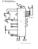
A voice signal from TEL line is encoded to digital data "TXDATA" by BBIC (IC501) in a base unit.
Then TXDATA goes to RF PART and it's modulated to 1.9 GHz. The RF signal is amplified and fed to a selected antenna.

As for a handset RF, RF signal is received in one antenna.
BBIC down-converts to 864 kHz IF signal from RX signal and demodulates it to digital data "RXDATA".
BBIC (IC1) converts RXDATA into a voice signal and outputs it to speaker.

Transmission

A voice signal from microphone is encoded to digital data "TXDATA" by BBIC (IC1) in a handset.
Then TXDATA goes to RF PART, and it's modulated to 1.9 GHz. The RF signal is amplified and fed to a antenna.

As for a base unit RF, RF signal is received in two antennas. 
BBIC (IC501) compares RF signal levels and selects the antenna to be used. Then BBIC down-converts to 864 kHz IF signal
from RX signal in the selected antenna, and demodulates it to digital data "RXDATA".
BBIC (IC501) converts RXDATA into a voice signal and outputs it to TEL line.

Summary of Contents for KX-TGA403LAT

Page 1: ...horized copying and distribution is a violation of law ORDER NO KM41006121CE Telephone Equipment Model No KX TG4021LAT KX TG4022LAT KX TG4023LAT KX TGA403LAT Expandable Digital Cordless Answering System T Black Metallic Version for Latin America ...

Page 2: ...2 KX TG4021LAT KX TG4022LAT KX TG4023LAT KX TGA403LAT ...

Page 3: ...set LCD 47 12 Measurements and Adjustments 48 12 1 Equipment Required 48 12 2 The Setting Method of JIG 48 12 3 Adjustment Standard Base Unit 51 12 4 Adjustment Standard Charger Unit 52 12 5 Adjustment Standard Handset 53 12 6 Things to Do after Replacing IC or X tal 54 12 7 Frequency Table 56 13 Miscellaneous 57 13 1 How to Replace the Flat Package IC 57 13 2 How to Replace the Shield Case 59 13 ...

Page 4: ...pe recommended by the manufacturer 3 Dispose of used batteries according to the manufacturer s Instructions 2 2 About Lead Free Solder PbF Pb free Note In the information below Pb the symbol for lead in the periodic table of elements will refer to standard solder or solder that contains lead We will use PbF solder when discussing the lead free solder used in our manufacturing process which is made...

Page 5: ...r Tin Zinc and Bismuth Sn Zn Bi Please check the manufacturer s specific instructions for the melting points of their products and any precautions for using their product with other materials The following lead free PbF solder wire sizes are recommended for service of this product 0 3 mm 0 6 mm and 1 0 mm 2 3 Discarding of P C Board When discarding P C Board delete all personal information such as...

Page 6: ... KX TGA403LAT 3 Specifications Note Design and specifications are subject to change without notice Note for Service Operation range Up to 300 m outdoors Up to 50 m indoors depending on the condition Analog telephone connection Telephone Line ...

Page 7: ...he 10 ms of voice data is transmitted 2 Handsets Link Traffic Bearer A link is established between base unit and handset The state where duplex communication is performed Handset doesn t make up duplex in no free RF channels because of interference 1 Dummy Bearer Base unit sends Dummy data to the all stand by state handsets Handsets receive that data for synchronization and monitoring request from...

Page 8: ...es it to digital data RXDATA BBIC IC1 converts RXDATA into a voice signal and outputs it to speaker Transmission A voice signal from microphone is encoded to digital data TXDATA by BBIC IC1 in a handset Then TXDATA goes to RF PART and it s modulated to 1 9 GHz The RF signal is amplified and fed to a antenna As for a base unit RF RF signal is received in two antennas BBIC IC501 compares RF signal l...

Page 9: ...UIT Q161 Q141 BELL DETECT HOOK BELL Q111 LIN LOUT RF_PART HSMIP HSMIN IC501 BBIC INUSE DETECT 2 INUSE DETECT 1 RECEIVE AMP DCIN 1 DCIN 2 IC302 VCCPA VBAT_APU VBAT VCC_FE VCC_IF VCC_VCO PDN DET 3 0V DOUBOUT SCL SDA WP VDD ANS_LED IC601 FLASH MEMORY IC611 EEPROM MEMORY KEYS R151 R152 R131 R133 Q171 VBAT DL CS MSG_LED KEY 1 3 KEY C D E SPOUTN SPOUTP 3 0 V REGULATOR IC331 RESET IC CLK DO STM CKM R371 ...

Page 10: ...10 KX TG4021LAT KX TG4022LAT KX TG4023LAT KX TGA403LAT 4 3 Block Diagram Base Unit_RF Part KX TG4021 4022 4023 BLOCK DIAGRAM Base Unit_RF Part DA801 ANT2 ANT1 TXON RXON RXp RXn ANT2 ANT1 TXp TXn ...

Page 11: ...mory DTMF Generator When the DTMF data from the handset is received the DTMF signal is output Synthesized Voice Pre recorded message The BBIC implements synthesized Voice utilizing the built in speech detector and a Flash Memory which stored the vocabulary Caller ID demodulation The BBIC implements monitor and demodulate the FSK DTMF signals that provide CID information from the Central Office Dig...

Page 12: ...023LAT KX TGA403LAT 4 4 4 Power Supply Circuit Reset Circuit The power supply voltage from AC adaptor is converted to VBAT 3 0V in IC302 And 3 0V for peripherals and analog part is insulated from VBAT by Doubler of BBIC Circuit Operation ...

Page 13: ...13 KX TG4021LAT KX TG4022LAT KX TG4023LAT KX TGA403LAT 4 4 4 1 Charge Circuit The voltage from the AC adaptor is supplied to the charge circuits ...

Page 14: ...C111 Q111 BBIC pin 5 BELL When the CPU BBIC detects a ring signal Q141 turns on thus providing an off hook condition active DC current flow through the circuit Following signal flow is the DC current flow T L101 D101 Q141 Q161 R163 R167 D101 L102 P101 R ON HOOK Circuit Q141 is open Q141 is connected as to cut the DC loop current and to cut the voice signal The unit is consequently in an on hook co...

Page 15: ... changes in the T R voltage Circuit Operation Parallel connection detection when on hook When on hook the voltage is monitored at pin 17 of IC501 There is no parallel connection if the voltage is 0 54 V or higher while a parallel connection is deemed to exist if the voltage is lower Parallel connection detection when off hook When off hook the voltage is monitored at pin 18 of IC501 the presence a...

Page 16: ... used The data for the caller ID from the telephone exchange is sent during the interval between the first and second rings of the bell signal The data from the telephone exchange is a modem signal which is modulated in an FSK Frequency Shift Keying format Data 1 is a 1200 Hz sine wave and data 0 is a 2200 Hz sine wave There are two types of the message format which can be received i e the single ...

Page 17: ...e customer is alerted to the new call so he she can use this information to decide whether to take the new call Function The telephone exchange transmits or receives CAS and ACK signals through each voice RX TX route Then FSK data and MARK data pass the following route Telephone Line P101 L101 L102 C121 C122 R121 R122 IC501 25 24 If the unit deems that a telephone connected in parallel is in use A...

Page 18: ...M BBIC RESET CHG_CTL CHG_DET WP CLK DATA P3_3 P3_7 P1_1 P1_4 CHARGE Q4 D7 MIC Receiver LED 3V Monitor SP LCD KEYS IC801 RF PART ANT1 X1 10 368 MHz EEPROM 3V BATTERY BELL BATTERY 3V BATTERY 3V KX TGA403 BLOCK DIAGRAM Handset KEY_LED Q7 LED KEY TXn Power_adj TXp VDD_PADRV PSEL PON TXON RXON RF_RXn RF_RXp CP_VOUT2 BATTERY VDDPA 1 8V VDD2 VDD1 3V Q2 1 8V C144 D1 ...

Page 19: ...19 KX TG4021LAT KX TG4022LAT KX TG4023LAT KX TGA403LAT 4 6 Block Diagram Handset_RF Part KX TGA403 BLOCK DIAGRAM Handset_RF Part DA801 TXON RXON ANT RF_RXn RF_RXp ...

Page 20: ...gnal All interfaces ex Key Detector Circuit Charge DC DC Converter EEPROM LCD RF Power Amp PLL Oscillator Detector Compress Expander Reception RF Power Amp IC801 Amplifier for transmission EEPROM IC3 Temporary operating parameters for RF etc 4 7 2 Power Supply Circuit Reset Circuit Circuit Operation When power on the Handset the voltage is as follows BATTERY 2 2 V 2 6 V BATT F1 Q2 1 8 V IC1 43pin ...

Page 21: ...d The charge current is controlled by switching Q9 of Handset Refer to Fig 101 in Power Supply Circuit Reset Circuit P 12 4 7 4 Battery Low Power Down Detector Circuit Operation Battery Low and Power Down are detected by BBIC which check the voltage from battery The detected voltage is as follows Battery Low Battery voltage V Batt 2 25 V 50 mV The BBIC detects this level and starts flashing Power ...

Page 22: ...peration Charger Unit Charge control is executed at handset side so that the operation when using charger is also controlled by handset Refer to Circuit Operation Handset P 20 The route for this is as follows DC pin of J1 F1 R1 CHARGE pad Handset CHARGE pad DC pin of J1 ...

Page 23: ...23 KX TG4021LAT KX TG4022LAT KX TG4023LAT KX TGA403LAT 4 9 Signal Route ...

Page 24: ...24 KX TG4021LAT KX TG4022LAT KX TG4023LAT KX TGA403LAT RF part signal route ...

Page 25: ...he Operating Instructions Instruction book on TSN Server 6 Installation Instructions Refer to the Operating Instructions Note You can download and refer to the Operating Instructions Instruction book on TSN Server 7 Operating Instructions Refer to the Operating Instructions Note You can download and refer to the Operating Instructions Instruction book on TSN Server ...

Page 26: ...26 KX TG4021LAT KX TG4022LAT KX TG4023LAT KX TGA403LAT 8 Test Mode 8 1 Engineering Mode 8 1 1 Base Unit ...

Page 27: ...below Items Address Default Data New Data Remarks Frequency 00 07 00 08 00 01 Use these items in a READ ONLY mode to confirm the contents Careless rewriting may cause serious damage to the computer system ID 00 02 00 06 Given value Desired Number hex Input Keys Desired Number hex Input Keys 0 0 A Flash 0 1 1 B Flash 1 C Flash 2 D Flash 3 E Flash 4 9 9 F Flash 5 ...

Page 28: ...28 KX TG4021LAT KX TG4022LAT KX TG4023LAT KX TGA403LAT 8 1 2 Handset ...

Page 29: ... confirm the contents Careless rewriting may cause serious damage to the handset Items Address Default Data New Data Possible Adjusted Value MAX hex Possible Adjusted Value MIN hex Remarks Battery Low 00 11 00 12 00 00 2 Frequency 00 07 00 08 00 01 ID 00 02 00 06 Given value Desired Number hex Input Keys Desired Number hex Input Keys 0 0 A Flash 0 1 1 B Flash 1 C Flash 2 D Flash 3 E Flash 4 9 9 F ...

Page 30: ...X TGA403LAT 9 Service Mode 9 1 How to Clear User Setting Handset Only Handset Press simultaneously until a beep sound is heard Then single handset is initialized The contents of user setting are reset to factory default Usage time is not cleared ...

Page 31: ...leshooting Guide 10 1 Troubleshooting Flowchart Cross Reference Check Power P 32 Check Playback P 34 Check Record P 33 Check Battery Charge P 34 Check Link P 35 Check the RF part P 37 Check Handset Transmission P 42 Check Handset Reception P 42 Check Caller ID P 42 ...

Page 32: ...1 Base Unit Cross Reference Power Supply Circuit Reset Circuit P 12 Note BBIC is IC501 1 Refer to Specifications P 6 for part number and supply voltage of AC adaptor 2 Refer to Circuit Board Base Unit_Main P 73 10 1 1 2 Handset Cross Reference Power Supply Circuit Reset Circuit P 20 ...

Page 33: ...TGA403LAT 10 1 2 Check Record 10 1 2 1 Base Unit A Not record Incoming Message Cross Reference Signal Route P 23 Telephone Line Interface P 14 Parallel Connection Detect Circuit Auto Disconnect Circuit P 15 Note Flash Memory is IC601 BBIC is IC501 ...

Page 34: ...ly Circuit Reset Circuit P 12 Note Flash Memory is IC601 BBIC is IC1 1 Refer to Circuit Board Base Unit_Main P 73 10 1 4 Check Battery Charge 10 1 4 1 Base Unit Cross Reference Charge Circuit P 13 10 1 4 2 Handset Cross Reference Check Power P 32 Charge Circuit P 21 10 1 4 3 Charger Unit Cross Reference Charge Circuit P 21 ...

Page 35: ...2 Check the RF part P 37 Note 1 How to adjust 3 0V Execute the command VDA Refer to Things to Do after Replacing IC or X tal P 54 for Base Unit 2 How to adjust the frequency of X501 To see the frequency execute the command SFR then check the TP_CKM IC501 57pin To adjust frequency send command SFR until the frequency counter becomes13 824 MHZ 55HZ ...

Page 36: ...set Circuit P 20 Check the RF part P 37 Note 1 How to adjust the frequency of X1 To see the frequency execute the command SFR then check the TP_CKM IC1 46pin To adjust frequency send command SFR until the frequency counter becomes10 368 MHz 55HZ Refer to Things to Do after Replacing IC or X tal P 55 for Handset ...

Page 37: ...LAT KX TGA403LAT 10 1 6 Check the RF part 10 1 6 1 Finding out the Defective part After All the Checkings or Repairing 1 Re register the checked handset to the checked base unit and Regular HS to Regular BU Note 1 HS Handset 2 BU Base Unit ...

Page 38: ...1LAT KX TG4022LAT KX TG4023LAT KX TGA403LAT 10 1 6 2 RF Check Flowchart Each item 1 6 of RF Check Flowchart corresponds to Check Table for RF part P 39 Please refer to the each item Note 1 Refer to Check Link P 35 ...

Page 39: ...BU 1 and RXDATA waveform of Regular HS by Digital Oscilloscope 1 Place Regular BU 15 cm away from a checked HS 2 Confirm TXDATA waveform of HS 2 and RXDATA waveform of Regular BU by Digital Oscilloscope 4 RX confirmation Regular HS BU Mode Test TX_Burst Mode BU HS Mode Test RX Mode 1 Place Regular HS 15 cm away from a checked BU 2 Confirm RXDATA waveform of BU 1 and TXDATA waveform of Regular HS b...

Page 40: ...1 3 At distance of about 20m between HS and BU Link OK TX Power of the HS is OK No Link TX Power of the HS is NG Range Confirmation RX TEST RX sensitivity check HS BU setting Checked unit High TX power 1 Regular unit Low TX power 1 1 Register Regular HS to BU to be checked 2 Set TX Power of the BU and the Regular HS according to CHART1 3 At distance of about 20m between HS and BU Link OK RX Sensit...

Page 41: ...41 KX TG4021LAT KX TG4022LAT KX TG4023LAT KX TGA403LAT 10 1 7 Registering a Handset to the Base Unit 10 1 8 Deregistering a Handset 10 1 9 Deregistering All Handsets by the Base Unit ...

Page 42: ...te When checking the RF part Refer to Check the RF part P 37 10 1 12 Check Caller ID Cross Reference Telephone Line Interface P 14 Calling Line Identification Caller ID Call Waiting Caller ID P 16 Note Make sure the format of the Caller ID service of the Telephone company that the customer subscribes to It is also recommended to confirm that the customer is really a subscriber of the service ...

Page 43: ...43 KX TG4021LAT KX TG4022LAT KX TG4023LAT KX TGA403LAT 11 Disassembly and Assembly Instructions 11 1 Disassembly Instructions 11 1 1 Base Unit ...

Page 44: ...44 KX TG4021LAT KX TG4022LAT KX TG4023LAT KX TGA403LAT ...

Page 45: ...45 KX TG4021LAT KX TG4022LAT KX TG4023LAT KX TGA403LAT 11 1 2 Handset ...

Page 46: ...46 KX TG4021LAT KX TG4022LAT KX TG4023LAT KX TGA403LAT 11 1 3 Charger Unit ...

Page 47: ...47 KX TG4021LAT KX TG4022LAT KX TG4023LAT KX TGA403LAT 11 2 How to Replace the Handset LCD Note The illustrations are simplified in this page They may differ from the actual product ...

Page 48: ...s recommended This equipment may be useful in order to precisely adjust like a mass production 12 2 The Setting Method of JIG Preparation Serial JIG cable PQZZ1CD300E PC which runs in DOS mode Batch file CD ROM for setting PNZZTG4021LA Note If you have the JIG Cable for TCD500 series PQZZ1CD505E change the following values of resistance Then you can use it as a JIG Cable for both TCD300 and TCD500...

Page 49: ...TGA403LAT 12 2 2 Connections Handset Connect the DC Power or Battery to BATT and BATT Connect the JIG cable GND black to GND Connect the JIG cable UTX yellow to UTX and URX red to URX Note COM port names may vary depending on what your PC calls it ...

Page 50: ...data of EEPROM Type rdeeprom 00 00 FF and the data from address 00 00 to FF is read out readid Read ID RFPI Type readid and the registered ID is read out writeid Write ID RFPI Type writeid 00 18 E0 0E 98 and the ID 0018 E0 0E 98 is written hookoff Off hook mode on Base Type hookoff hookon On hook mode on Base Type hookon getchk Read checksum Type getchk wreeprom Write the data of EEPROM Type wreep...

Page 51: ...R112 R178 VCCA VREF R166 R164 R161 R136 VDDC R151 R152 R115 R121 L371 L1T L1R L476 L474 L372 L362 IC601 IC302 IC611 RA151 RA504 D361 D473 D472 D153 D133 D363 Q161 Q601 C142 C513 C167 C512 C186 C184 C601 C479 C307 C301 C332 C521 C133 C123 C472 C473 C475 C120 C124 C151 C525 C524 C611 C115 C168 C126 C661 R165 F301 DCP DCM R512 R507 R307 R607 R601 R304 R305 R301 R505 R506 R334 R604 R181 R162 R503 R167...

Page 52: ...3LAT 12 4 Adjustment Standard Charger Unit When connecting the simulator equipment for checking please refer to below 12 4 1 Bottom View TP4 TP3 1 2 J1 A F1 PbF PNLP1029YA PQUP11532Y Charge Charge 12 2 W Digital Volt Meter DC POWER DC 6 5 V TP3 TP4 GND ...

Page 53: ...1 R330 R3 R8 R4 L802 IC3 TP_ANT1 RA800 RA4 RA40 CP3 0V CP4 0V D22 D21 D13 RED BLK R E D B L K D14 D400 D7 D3 D4 Q401 POWER Q400 Q11 Q12 GND C580 C187 C186 C204 C827 C881 C819 C45 C46 C825 C809 C810 C861 C 8 0 8 C812 C806 C138 C139 C803 C805 C47 C822 C826 C820 C860 C182 C49 C50 C188 C12 C13 C11 C96 C18 C17 C97 C38 C35 C121 C150 C1 C2 C172 C75 C74 C3 X1 MIC R232 R55 SPEAKER R233 R806 R64 R28 R403 R4...

Page 54: ...Method of JIG P 48 Items How to download Required adjustment EEPROM IC611 Adjusted parameter data is stored in memory country version batch file default batch file etc 1 Change the address 0001 of EEPROM to 55 to download the data 2 Default batch file Execute the command default bat 3 Country version batch file Execute the command TG4021USLArevXXX_YYY bat 1 4 Clock adjustment X tal X1 System clock...

Page 55: ... sendchar LED 0 sendchar CRX 0 1 sendchar AD1 It assumes that the return value is XX a 6c XX 71 No need to adjust b XX 6A 6B Need to adjust XX 72 74 Need to adjust Write AD value of 2 25 V to EEPROM ex read data XX 6A write data YY 6A read data XX 73 write data YY 73 EEPROM 0009 Low Voltage write YY Execute the command wreeprom 00 09 01 YY EEPROM 000A No Voltage write YY 1D Execute the command xwr...

Page 56: ... TG4021LAT KX TG4022LAT KX TG4023LAT KX TGA403LAT 12 7 Frequency Table Ch hex TX RX Frequency MHz Channel 0 00 1928 448 Channel 1 01 1926 720 Channel 2 02 1924 992 Channel 3 03 1923 264 Channel 4 04 1921 536 ...

Page 57: ... overheat and damage the PCB foil Flux Recommended Flux Specific Gravity 0 82 Type RMA lower residue non cleaning type Note See About Lead Free Solder PbF Pb free P 4 13 1 2 How to Remove the IC 1 Put plenty of solder on the IC pins so that the pins can be completely covered Note If the IC pins are not soldered enough you may give pressure to the P C board when cutting the pins with a cutter 2 Mak...

Page 58: ...e accuracy of the IC setting with the corresponding soldering foil 2 Apply flux to all pins of the FLAT PACKAGE IC 3 Solder the pins sliding the soldering iron in the direction of the arrow 13 1 4 How to Remove a Solder Bridge 1 Lightly resolder the bridged portion 2 Remove the remaining solder along the pins using a soldering iron as shown in the figure below ...

Page 59: ...Hot Air Desoldering Tool Temperature 608 F 68 F 320 C 20 C 13 2 2 Caution To replace the IC efficiently choose the right sized nozzle of the hot air desoldering tool that matches the IC package Be careful about the temperature of the hot air desoldering tool not to damage the PCB and or IC 13 2 3 How to Remove the Shield Case Note If you don t have special tools ex Hot air disordering tool conduct...

Page 60: ...TG4023LAT KX TGA403LAT 13 2 4 How to Install the Shield Case Note If you don t have special tools ex Hot air disordering tool conduct the following operations Shield case s No PNMC1013Z 1 Put the shield case 2 Solder the surroundings ...

Page 61: ...8 F 320 C 20 C 13 3 2 Caution To replace the IC efficiently choose the right sized nozzle of the hot air desoldering tool that matches the IC package Be careful about the temperature of the hot air desoldering tool not to damage the PCB and or IC 13 3 3 How to Remove the IC 1 Heat the IC with a hot air desoldering tool through the P C Board 2 Pick up the IC with tweezers etc when the solder is mel...

Page 62: ... placing the IC the positioning should be done very carefully 3 Heat the IC with a hot air desoldering tool through the P C Board until the solder on IC bottom is melted Note Be sure to place it precisely controlling the air volume of the hot air desoldering tool 4 After soldering confirm there are no short and open circuits with visual inspection 13 3 5 How to Remove a Solder Bridge When a Solder...

Page 63: ...63 KX TG4021LAT KX TG4022LAT KX TG4023LAT KX TGA403LAT 13 4 Terminal Guide of the ICs Transistors and Diodes 13 4 1 Base Unit 13 4 2 Handset ...

Page 64: ...with the development of new technology 14 1 2 Handset Schematic Diagram Handset_Main Notes 1 DC voltage measurements are taken with an oscilloscope or a tester with a ground 2 The schematic diagrams may be modified at any time with the development of new technology 14 1 3 Charger Unit Schematic Diagram Charger Unit Notes 1 DC voltage measurements are taken with voltmeter from the negative voltage ...

Page 65: ...65 KX TG4021LAT KX TG4022LAT KX TG4023LAT KX TGA403LAT Memo ...

Page 66: ...Xn RXp GND STM CKM P15 GND GND GND GND CL1 CL2 Q651 1 B1 2 E 3 B2 5 C1 4 C2 C893 3p GND GND GND GND TDI TMS TCK TDO C895 1 2p C896 2 2p C859 2 2p C805 2 7p C806 2 7p C820 1 5p C863 1 5p R502 33 RTCK C660 NC C810 2 4p C813 2p L809 7 5n C891 5p C892 5p C811 10p C826 10p C822 10p C825 10p C653 NC C654 NC C812 0 9p C827 10p GND C894 2 2p R651 680 R652 680 R507 NC 3 0V R512 1k 45 TXp 46 RXp 47 RXn 48 G...

Page 67: ...ROM 1 A0 2 A1 3 A2 4 GND 5 SDA 6 SCL 7 WP 8 VCC R136 NC CHG 2 CHG 2 D363 NC A K GND C321 1u Q161 B C E C502 10u C505 10u C511 10u C341 330u ZA1 NC 1 2 6 7 9 11 3 4 5 8 10 12 C472 NC C475 NC C473 NC C530 10p C307 NC C522 10p C343 10p C523 NC C524 NC C525 NC R176 100 R172 100k C175 1000p R160 910 C178 0 022u C161 10u C176 10u C173 K0 22u R177 NC Q171 B C E R171 22 C174 NC R175 560 C164 NC R181 0 C17...

Page 68: ...ase Unit_Operation KX TG4021 4022 4023 SCHEMATIC DIAGRAM Base Unit_Operation NC No Components ANS1 1 2 STOP 1 2 ERASE 1 2 MSG2 1 2 MSG1 1 2 RPT 1 2 SKIP 1 2 UP 1 2 DOWN 1 2 LOCAT INT 1 2 LED902 A K LED901 A K MEG_LED KEYIN2 KEYS_B ANS_LED KEYS_E KEYS_C KEYIN1 2APVCC KEYIN3 KEYS_D ...

Page 69: ...69 KX TG4021LAT KX TG4022LAT KX TG4023LAT KX TGA403LAT Memo ...

Page 70: ...ND NC C38 NC C138 NC C139 LED5 LED7 LED4 LED6 LED8 LED9 X1 10 368M 1 3 2 LED21 NC NC NC NC R249 1 VSS_LNA1 2 RF_RXp 21 CIDINp VREFp 3 RF_RXn 4 VSS_LNA2 5 RFP1 6 RFP0 7 REF_RES 8 AVS_XTAL 22 RINGp P3_7 23 RINGn P3_6 24 RINGOUT RINGING P3_5 25 PARADET P3_4 26 ADC0 P3_3 27 ADC1 INT0 P1_0 28 NTC ADC2 41 CP_C2y 42 CP_VOUT1 LED1 43 CP_VOUT2 LED2 44 PON P1_6 45 VDD1 46 P2_7 BXTAL 81 GND 9 XTAL2 10 XTAL1 ...

Page 71: ...3 820k R231 430k R232 0 1 C204 NC R233 1k RA800 1 2 3 4 NC R236 NC C206 CN51 13 CAP1 CN51 14 VSS CN51 15 RES CN51 7 V0 CN51 9 VOUT CN51 4 SI CN51 5 SCL CN51 10 CAP2 CN51 8 VR CN51 3 CS CN51 11 CAP2 CN51 1 GND CN51 16 GND CN51 12 CAP1 CN51 2 RS CN51 6 VDD Q880 NC GND GND GND Power_adj NC C881 NC R880 2p C804 2p C802 1 5p C803 GND GND GND GND RECEIVER 1 2 SP PHONE_SPEAKER 1 2 J33p C107 10p C809 10p ...

Page 72: ...72 KX TG4021LAT KX TG4022LAT KX TG4023LAT KX TGA403LAT 14 5 Schematic Diagram Charger Unit J1 2 1 TP3 G TP2 TP1 TP4 R1 12 F1 SCHEMATIC DIAGRAM Charger Unit ...

Page 73: ...121 L371 L1T L1R L476 L474 L372 L362 IC601 IC302 IC611 RA151 RA504 D361 D473 D472 D153 D133 D363 Q161 Q601 C142 C513 C167 C512 C186 C184 C601 C479 C307 C301 C332 C521 C133 C123 C472 C473 C475 C120 C124 C151 C525 C524 C611 C115 C168 C126 C661 R165 F301 DCP DCM R512 R507 R307 R607 R601 R304 R305 R301 R505 R506 R334 R604 R181 R162 R503 R167 R163 R122 L361 RA502 D142 D143 CHG 2 CHG 2 KX TG4021 4022 40...

Page 74: ...14 R372 R172 R177 R332 KEYS_E 1 10 KEYS_D KEYS_C KEYIN3 KEYIN2 KEYIN1 NC ANS_LED MSG_LED 2APVCC ZA1 R331 IC501 IC331 SW1 Q141 Q143 Q111 Q651 C176 C113 C174 C161 C164 C173 C509 C508 C812 C306 C515 C304 C519 C305 C303 C518 C516 C805 C859 C896 C342 C503 C660 C659 C658 C656 C655 C654 C653 C652 C651 C172 C506 C505 C185 X501 R160 R111 R113 R175 R176 R171 R509 R806 R891 R144 R142 R892 R807 R333 R652 R651...

Page 75: ...4023LAT KX TGA403LAT 15 2 Circuit Board Base Unit_Operation KX TG4021 4022 4023 CIRCUIT BOARD Base Unit_Operation Component View A PNLB1753Z KX TG4021 31H PbF LED902 LED901 STOP DOWN RPT MSG1 MSG3 MSG2 MSG4 LOCAT INT SKIP ANS1 UP ERASE ...

Page 76: ...76 KX TG4021LAT KX TG4022LAT KX TG4023LAT KX TGA403LAT Memo ...

Page 77: ... R37 R36 R20 CLK 1 8V R7 R30 F1 R2 R332 R331 R330 R3 R8 R4 L802 IC3 TP_ANT1 RA800 RA4 RA40 CP3 0V CP4 0V D22 D21 D13 RED BLK R E D B L K D14 D400 D7 D3 D4 Q401 POWER Q400 Q11 Q12 GND C580 C187 C186 C204 C827 C881 C819 C45 C46 C825 C809 C810 C861 C 8 0 8 C812 C806 C138 C139 C803 C805 C47 C822 C826 C820 C860 C182 C49 C50 C188 C12 C13 C11 C96 C18 C17 C97 C38 C35 C121 C150 C1 C2 C172 C75 C74 C3 X1 MIC...

Page 78: ..._Main Bottom View 1 2 PbF PNLB1734Y 12 1 3 SP R DOWN LEFT SOFT_A SOFT_B R52 R51 TGA250XX TGA251XX TGA403XX TGA650XX TGA651XX KX TGA650XX KX TGA651XX KX TGA250XX KX TGA251XX KX TGA403XX CN51 CN5 SOFT_C RIGHT TALK UP S1 4 5 6 7 MIC 8 9 LED4 LED7 LED12 LED21 LED22 LED23 LED1 LED2 LED3 LED8 LED6 LED9 LED5 0 A ...

Page 79: ...03LAT 15 4 Circuit Board Charger Unit 15 4 1 Component View 15 4 2 Bottom View J1 R1 A PQUP11532Y PbF PNLP1029YA CIRCUIT BOARD Charger unit Component View TP4 TP3 1 2 J1 A F1 PbF PNLP1029YA PQUP11532Y CIRCUIT BOARD Charger unit Bottom View TP4 GND TP3 ...

Page 80: ...Replacement Parts List 16 1 Cabinet and Electrical Parts Base Unit Note 1 The SPACERs No 14 are cut from the excess parts of SPACER No 108 of Cabinet and Electrical Parts Handset P 81 A A A PCB2 13 13 7 12 1 E1 14 1 4 5 6 2 3 14 1 10 11 9 8 15 Ref No Figure A 2 6 x 8mm 16 PCB1 ...

Page 81: ...hargeable Ni MH battery HHR 4DPA or HHR 4MRT is available through sales route of Panasonic 3 Attach the SPACER No 119 to the exact location described above 102 103 104 E103 E105 E102 E101 1 111 115 116 105 106 110 113 B 2 118 120 119 3 101 109 E104 112 E106 B E107 MIC100 PCB100 108 B 117 114 107 Spacer No 119 Battery cover Put it in the center Stick it between ribs Ref No Ǿ2 8 mm B Figure ...

Page 82: ...82 KX TG4021LAT KX TG4022LAT KX TG4023LAT KX TGA403LAT 16 3 Cabinet and Electrical Parts Charger Unit B 200 200 1 200 3 200 4 200 2 B PCB200 Ref No B Figure ...

Page 83: ...83 KX TG4021LAT KX TG4022LAT KX TG4023LAT KX TGA403LAT 16 4 Accessories A2 A3 A1 ...

Page 84: ...1047Z CHARGE TERMINAL 9 PNBC1307Z1 BUTTON NAVIGATOR KEY PS HB 10 PNHR1259Z GUIDE BUTTON HOLDER PS HB 11 PNBC1308Z1 BUTTON MESSAGE AS HB 12 PNJK1079Z KEYBOARD SWITCH 13 PNLA1030Z ANTENNA 14 PNYE1027Z SPACER ANTENNA 15 PNKF1099Y1 CABINET COVER PS HB 16 PQHA10023Z RUBBER PARTS FOOT CUSHION Safety Ref No Part No Part Name Description Remarks PCB1 PNWP14021LAH MAIN P C BOARD ASS Y RTL ICs IC302 C0CBAYG...

Page 85: ...UE1H100DCQ 10p C501 ECUE1A104KBQ 0 1 C502 ECJ1VB0G106M 10 C503 ECJ1VB0G106M 10 C504 ECUE0J105KBQ 1 C505 ECJ1VB0G106M 10 C506 ECUV1A105KBV 1 Safety Ref No Part No Part Name Description Remarks C507 ECUV1A225KB 2 2 C508 ECUE1H100DCQ 10p C509 ECUE1H120JCQ 12p C510 ECUV1A105KBV 1 C511 ECJ1VB0G106M 10 C512 ECUE1A104KBQ 0 1 C513 ECUV1A225KB 2 2 C514 ECUE1A104KBQ 0 1 C515 ECUV1A105KBV 1 C516 ECUE1A104KBQ...

Page 86: ...0240004 RESISTOR ARRAY S RA4 D1H433220001 RESISTOR ARRAY RA30 D1H83314A013 RESISTOR ARRAY S RA31 D1H433120001 RESISTOR ARRAY RA32 EXB28V121JX RESISTOR ARRAY RA40 EXB28V103 RESISTOR ARRAY RA61 D1H422120001 RESISTOR ARRAY RA800 D1H410220001 RESISTOR ARRAY IC FILTERS Safety Ref No Part No Part Name Description Remarks L46 J0JDC0000045 IC FILTER L47 J0JDC0000045 IC FILTER RESISTORS R3 ERJ2GEJ102 1k S ...

Page 87: ...00A723 10p C861 F1G1H3R0A480 3p OTHERS MIC100 L0CBAY000032 MICROPHONE E101 L5DYBYY00012 LIQUID CRYSTAL DISPLAY 3 E102 PNHR1247Z TRANSPARENT PLATE LCD PMMA HB E103 PNHR1246Z GUIDE LCD ABS HB E104 PNHX1254Z COVER LCD E105 PNLA1020Z ANTENNA E106 PNMC1013Z CASE MAGNETIC SHIELD 4 E107 PNVE1002Z BATTERY TERMINAL X1 H0J103500033 CRYSTAL OSCILLATOR 2 Safety Ref No Part No Part Name Description Remarks 200...

Reviews: