background image

 1 

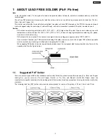
ABOUT LEAD FREE SOLDER (PbF: Pb free) 

3

 1.1. 

Suggested PbF Solder 

3

 1.2. 

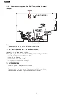
How to recognize that Pb Free solder is used 

4

 2 

FOR SERVICE TECHNICIANS 

4

 3 

CAUTION 

4

 4 

BATTERY 

5

 4.1. 

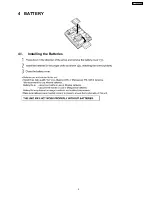
Installing the Batteries 

5

 4.2. 

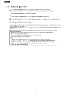
Battery Replacement 

6

 5 

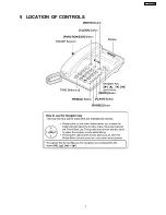
LOCATION OF CONTROLS 

7

 6 

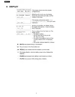
DISPLAY 

8

 7 

SETTINGS 

9

 7.1. 

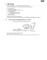
Connecting the Handset/Telephone Line Cord 

9

 7.2. 

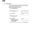
Dialing Mode 

10

 7.3. 

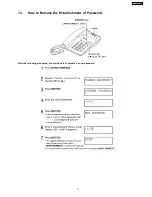
How to Release the Establishment of Password 

11

 7.4. 

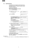
Call Restriction 

12

 8 

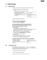
OPERATIONS 

13

 8.1. 

Making Calls 

13

 8.2. 

Answering Calls 

13

 8.3. 

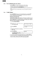
For Call Waiting Service Users 

14

 8.4. 

FLASH Button 

14

 8.5. 

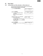
Phone Book 

15

 9 

TROUBLESHOOTING 

22

 10 DISASSEMBLY INSTRUCTIONS 

24

 11 TROUBLESHOOTING GUIDE 

25

 11.1. Service Hints 

25

 11.2. Pulse Dialing Problems 

25

 11.3. Tone Dialing Problems (handset) 

25

 11.4. No Ringing Sound When Ring Signal is Input 

26

 12 TEST MODE 

27

 13 BLOCK DIAGRAM 

28

 14 CIRCUIT OPERATION 

29

 14.1. Bell Detector Circuit 

29

 14.2. Line Interface 

29

 14.3. MODULE BLOCK DIAGRAM 

29

 14.4. Caller ID Detect Circuit 

31

 15 IC BLOCK DIAGRAM 

32

 15.1. IC502 

32

 15.2. CPU DATA (IC502) 

33

 15.3. RINGER IC (IC2) 

34

 15.4. EEPROM (IC802) 

34

 16 HOW TO REPLACE FLAT PACKAGE IC 

35

 16.1. PREPARATION 

35

 16.2. FLAT PACKAGE IC REMOVALPROCEDURE 

35

 16.3. FLAT PACKAGE IC INSTALLATION PROCEDURE 

36

 16.4. BRIDGE MODIFICATION PROCEDURE 

36

 17 CABINET AND ELECTRICAL PARTS 

37

 18 ACCESSORIES AND PACKING MATERIALS 

38

 19 TERMINAL GUIDE OF THE ICs, TRANSISTORS AND DIODES


39

 20 REPLACEMENT PARTS LIST 

40

 20.1. Base Unit 

40

 20.2. Accessories and Packing Materials 

42

 21 FOR SCHEMATIC DIAGRAM 

43

 22 SCHEMATIC DIAGRAM 

44

 22.1. Memo 

46

 23 CIRCUIT BOARD 

47

 23.1. Component View 

47

 23.2. Flow Solder Side View 

48

Note:

Because CONTENTS 4 to 9 are the extracts from the Operating Instructions of this model, they are subject to change without
notice. Please refer to the original Operating Instructions for further information.

CONTENTS

 Page 

Page

2

KX-TSC11AGW

Summary of Contents for KX-TSC11AGW

Page 1: ...ic Communications Co Ltd All rights reserved Unauthorized copying and distribution is a violation of law KX TSC11AGW Integrated Telephone System White Version for Argentina Telephone Equipment ORDER NO KM40504678CE ...

Page 2: ...IRCUIT OPERATION 29 14 1 Bell Detector Circuit 29 14 2 Line Interface 29 14 3 MODULE BLOCK DIAGRAM 29 14 4 Caller ID Detect Circuit 31 15 IC BLOCK DIAGRAM 32 15 1 IC502 32 15 2 CPU DATA IC502 33 15 3 RINGER IC IC2 34 15 4 EEPROM IC802 34 16 HOW TO REPLACE FLAT PACKAGE IC 35 16 1 PREPARATION 35 16 2 FLAT PACKAGE IC REMOVALPROCEDURE 35 16 3 FLAT PACKAGE IC INSTALLATION PROCEDURE 36 16 4 BRIDGE MODIF...

Page 3: ... be careful not to heat too long PbF solder will tend to splash if it is heated much higher than its melting point approximately 1100 F 600 C If you must use Pb solder on a PCB manufactured using PbF solder remove as much of the original PbF solder as possible and be sure that any remaining is melted prior to applying the Pb solder When applying PbF solder to double layered boards please check the...

Page 4: ... VR481 YELLOW PQUP11270Z Component View Note The location of the PbF marks is subject to change without notice 2 FOR SERVICE TECHNICIANS ICs and LSIs are vulnerable to static electricity When replacing the following precautions will help prevent recurring malfunctions 1 Cover the plastic parts boxes with aluminum foil 2 Ground the soldering irons 3 Use a conductive mat on the worktable 4 Do not gr...

Page 5: ...4 BATTERY 4 1 Installing the Batteries 5 KX TSC11AGW ...

Page 6: ...4 2 Battery Replacement 6 KX TSC11AGW ...

Page 7: ...5 LOCATION OF CONTROLS 7 KX TSC11AGW ...

Page 8: ...6 DISPLAY 8 KX TSC11AGW ...

Page 9: ...ephone Line Cord Use only a Panasonic Handset for the KX TSC11AGW Use only a telephone line cord included with the unit If your unit is connected to a PBX which does not support Caller ID services you cannot access those services 9 KX TSC11AGW ...

Page 10: ...7 2 Dialing Mode 10 KX TSC11AGW ...

Page 11: ...7 3 How to Release the Establishment of Password After the following procedure you will be able to establish a new password 11 KX TSC11AGW ...

Page 12: ...7 4 Call Restriction For Service Hint If the current password is forgotten refer to How to Release the Establishment of Password P 11 12 KX TSC11AGW ...

Page 13: ...8 OPERATIONS 8 1 Making Calls 8 2 Answering Calls 13 KX TSC11AGW ...

Page 14: ...8 3 For Call Waiting Service Users 8 4 FLASH Button 14 KX TSC11AGW ...

Page 15: ...8 5 Phone Book 8 5 1 Storing Names and Phone Numbers in Phone Book List 15 KX TSC11AGW ...

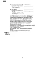
Page 16: ...Cross Reference Erasing P 21 Chain Dial P 20 16 KX TSC11AGW ...

Page 17: ...17 KX TSC11AGW ...

Page 18: ...8 5 2 Storing Caller List Information in the Phone Book List Cross Reference Erasing P 21 18 KX TSC11AGW ...

Page 19: ...8 5 3 Dialing from the Phone Book 19 KX TSC11AGW ...

Page 20: ...8 5 4 Chain Dial Cross Reference Dialing from the Phone Book P 19 20 KX TSC11AGW ...

Page 21: ...8 5 5 Editing Cross Reference Dialing from the Phone Book P 19 8 5 6 Erasing Cross Reference Dialing from the Phone Book P 19 21 KX TSC11AGW ...

Page 22: ...9 TROUBLESHOOTING Cross Reference 1 Battery Replacement P 6 2 Dialing Mode P 10 3 Call Restriction P 12 22 KX TSC11AGW ...

Page 23: ...23 KX TSC11AGW ...

Page 24: ...10 DISASSEMBLY INSTRUCTIONS Shown in Fig To remove Remove 1 Cabinet Cover Screws 2 6 12 A 4 2 Main P C Board Screws 2 0 6 B 6 Screws 2 6 10 C 4 Main P C Board 24 KX TSC11AGW ...

Page 25: ...11 TROUBLESHOOTING GUIDE Make sure batteries are installed for proper operation before troubleshooting 11 1 Service Hints 11 2 Pulse Dialing Problems 11 3 Tone Dialing Problems handset 25 KX TSC11AGW ...

Page 26: ...11 4 No Ringing Sound When Ring Signal is Input 26 KX TSC11AGW ...

Page 27: ...12 TEST MODE Note After the test the unit will be back to the factory preset mode 27 KX TSC11AGW ...

Page 28: ...3 Q801 Reset IC D302 PC1 IC2 Battery 4 5V Q102 Q104 IC802 Q108 Handset Regulator RINGER IC Line ON OFF IC502 CPU Ring_Det LCD EEPROM Transmit Amp Handset Amp Receiving Handset Amp Sending IC301 Batt Low VDD STOP C ID Reset Keyboard IC302 IC803 KX TSC11 BLOCK DIAGRAM KX TSC11AGW 28 ...

Page 29: ...ches between high and low logic is output from pin 73 of the CPU This switches the line loop on and off generating the dial pulse signal 14 3 MODULE BLOCK DIAGRAM 14 3 1 Telephone Line Interface 14 3 1 1 Circuit operation On hook Q102 is open Q102 is connected as to cut DC loop current and cut the voice signal Off hook Q102 turns on thus providing an off hook condition active DC current flow throu...

Page 30: ...PU when the batteries are installed 14 3 2 2 Circuit operation When the batteries are inserted into the unit then the voltage is regulated by IC302 and power is supplied to the CPU The unit starts operating soon after the voltage goes beyond point A in the voltage diagram 30 KX TSC11AGW ...

Page 31: ... the operation of this circuit assumes that a caller ID service contract has been entered for the circuit being used The Caller ID data from exchange is supplied to the telephone using the method of FSK and displayed on LCD of the unit FSK Frequency Shift Keying format 14 4 2 Circuit operation Caller ID Caller ID signal is sent through the circuit via the following path TEL Line C501 C502 R551 R55...

Page 32: ...15 IC BLOCK DIAGRAM 15 1 IC502 32 KX TSC11AGW ...

Page 33: ...15 2 CPU DATA IC502 33 KX TSC11AGW ...

Page 34: ...s and the mutual data between Master Device and Slave Device the mutual This terminal needs the pull up resistance external because output circuit of SDA uses Open Drain 3 A0 A1 A2 A0 A1 and A2 terminal is not used 4 WP WP terminal controls writing action It is possible to do only reading action when high level input and it is possible to do reading and writing action when low level input 34 KX TS...

Page 35: ...lux Specific Gravity 0 82 Type RMA lower residue non cleaning type Note See ABOUT LEAD FREE SOLDER PbF Pb free P 3 16 2 FLAT PACKAGE IC REMOVALPROCEDURE 1 Put plenty of solder on the IC pins so that the pins can be completely covered Note If the IC pins are not soldered enough you may give pressure to the P C board when cutting the pins with a cutter 2 Make a few cuts into the joint between the IC...

Page 36: ...g with the corresponding soldering foil 2 Apply flux to all pins of the FLAT PACKAGE IC 3 Solder the pins sliding the soldering iron in the direction of the arrow 16 4 BRIDGE MODIFICATION PROCEDURE 1 Lightly resolder the bridged portion 2 Remove the remaining solder along the pins using a soldering iron as shown in the figure below 36 KX TSC11AGW ...

Page 37: ...17 CABINET AND ELECTRICAL PARTS Note 1 Batteries are not included 37 KX TSC11AGW ...

Page 38: ...18 ACCESSORIES AND PACKING MATERIALS 38 KX TSC11AGW ...

Page 39: ...19 TERMINAL GUIDE OF THE ICs TRANSISTORS AND DIODES 39 KX TSC11AGW ...

Page 40: ...ERMINAL 12 PQJC314Y BATTERY TERMINAL 13 PQHX11312Z SPACER 14 PQQT22895Z LABEL DIAL MODE 20 1 2 Main P C Board Parts Ref No Part No Part Name Description Remarks PCB1 PQWPTSC11AGH MAIN P C BOARD ASS Y RTL ICs IC2 C1CA00000254 IC IC301 PQVIPS3238NT IC S IC302 C0CBABE00023 IC IC502 C2CBHF000411 IC IC802 PQWITSC11AGH IC IC803 PQVIPS3327UT IC TRANSISTORS Q102 2SA1626 TRANSISTOR SI Q104 PQVT2N6517CA TRA...

Page 41: ...2 4 7K R431 ERJ3GEYJ335 3 3M R432 ERJ3GEYJ474 470K R482 ERJ3GEYJ103 10K R484 ERJ3GEYJ104 100K Ref No Part No Part Name Description Remarks R485 ERJ3GEYJ103 10K R486 ERJ3GEYJ103 10K R487 ERJ3GEY0R00 0 R520 ERJ3GEYJ105 1M R551 PQ4R10XJ103 10K S R552 PQ4R10XJ103 10K S R553 ERJ3GEYJ333 33K R561 PQ4R10XJ335 3 3M S R562 PQ4R10XJ473 47K S R563 PQ4R10XJ335 3 3M S R564 ERJ3GEYJ103 10K R565 ERJ3GEYJ103 10K ...

Page 42: ...KA100 10 C820 ECEA0JKA101 100 C822 ECUV1C104KBV 0 1 C830 ECUV1C104KBV 0 1 OTHERS E1 PQGP10263Y1 PANEL LCD S E2 L5ACAHC00008 LIQUID CRYSTAL DISPLAY E3 PQJE10110Z CONNECTOR ZEBRA E4 PQHR10937Z SPACER LCD PC1 B3PAA0000330 PHOTO COUPLER S SA101 PQVDDSS301L VARISTOR SURGE ABSORBER S X801 H0A327200132 CRYSTAL OSCILLATOR S POS101 PFRT002 THERMISTOR S 20 2 Accessories and Packing Materials Ref No Part No ...

Page 43: ...condition 6 No Mack Handset Mode 7 This schematic diagram may be modified at any time with the development of new technology 8 The shades area on this schematic diagram incorporates special features important for protection from fire and electrical shock hazards 9 When servicing it is essential that only manufacture s specified parts be used for the critical components in the shaded areas of the s...

Page 44: ... SEG1 124 KXTB2 SEG2 125 KXTB3 SEG3 126 NC 127 NC 128 NC 72 Wake up 71 BATT_OUT 70 Relay 69 120KLoad lineSeiz 68 RCDC 67 NC 66 NC 65 NC 63 NC 62 NC 61 Ring_Det 60 Backup E12V 59 BATt LOW 104 AVDD 106 COM0 107 COM1 108 COM2 38 SEG32 37 SEG31 36 SEG30 35 NC 33 NC 105 LVDD 31 NC 32 NC 34 NC 64 NC 103 VR2 D_lock REDIAL PAUSE FLASH D600 D601 D602 D603 D604 D605 C813 NC NC R999 NC C999 R921 39K R810 NC ...

Page 45: ...5 C116 NC R120 330K C410 50V4 7 C557 0 01U R487 0 A B NC IC501 1 2 3 4 5 6 7 8 C502 0 01u 500V C501 0 01u 500V C555 k330P C106 16V47 C111 16V10 C2 50V10 C304 6 3V1000 C503 K4700P C504 K4700P D302 R112 1 5K R126 100K 22K R813 J007 12 5mm J012 17 5mm J002 15mm J015 7 5mm PCB J006 12 5mm J016 25mm J013 7 5mm J001 17 5mm J009 17 5mm J004 5mm J011 20mm J010 15mm J017 25mm J003 17 5mm J008 5mm J014 10mm...

Page 46: ...22 1 Memo 46 KX TSC11AGW ...

Page 47: ...GREEN C501 C502 R161 R1 D302 D102 C302 C107 C2 C1 IC2 SW1 C111 C304 Q108 C161 J002 C409 C420 C106 R114 D105 J009 J010 J006 J014 J013 L102 L101 R126 C101 C814 C819 X801 POS101 SA101 JJ101 PC1 5 8 1 4 SW101 J3 J1 PbF PQUP11270Z J2 J4 C410 VR401 Q103 Q102 Q106 Q104 Q181 R106 J001 J004 VR402 VR481 YELLOW KX TSC11 CIRCUIT BOARD Component View A KX TSC11AGW 47 ...

Page 48: ... R415 R416 R426 R427 R484 R485 R420 R421 R116 R206 R916 R120 TP9 TP1 C813 C116 R123 Q105 IC501 R105 R121 R122 R201 C204 R922 C203 R205 R552 R551 R513 R514 R565 C816 C809 C807 C808 R564 R481 R553 R554 R482 R423 R424 R425 R402 R409 R428 R208 R207 R202 R203 D915 D202 R109 D106 R164 R117 R112 R110 R165 R111 C201 Q107 IC302 IC201 R119 R166 R167 R115 R118 R113 R104 R107 R108 R103 TP3 TP101 TP102 TP2 D10...

Page 49: ...49 KX TSC11AGW I N N KXTSC11AGW ...

Reviews: