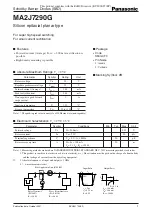

Schottky Barrier Diodes (SBD)
1
Publication date: October 2007
SKH00172AED
This product complies with the RoHS Directive (EU 2002/95/EC).
MA2J7290G
Silicon epitaxial planar type
For super high speed switching
For small current rectification
■
Features
•
Forward current (Average) I
F(AV)
=
200 mA rectification is
possible
•
High-density mounting is possible
■
Absolute Maximum Ratings
T
a
=
25
°
C
Parameter
Symbol
Rating
Unit
Reverse voltage
V
R
30
V
Repetitive peak reverse voltage
V
RRM
30
V
Forward current (Average)
I
F(AV)
200
mA
Peak forward current
I
FM
300
mA
Non-repetitive peak forward
I
FSM
1
A
surge current
*
Junction temperature
T
j
150
°
C
Storage temperature
T
stg
−
55 to
+
150
°
C
Parameter
Symbol
Conditions
Min
Typ
Max
Unit
Forward voltage
V
F
I
F
=
200 mA
0.55
V
Reverse current
I
R
V
R
=
30 V
50
µ
A
Terminal capacitance
C
t
V
R
=
0 V, f
=
1 MHz
30
pF
Reverse recovery time
*
t
rr
I
F
=
I
R
=
100 mA
3.0
ns
I
rr
=
0.1 I
R
, R
L
=
100
Ω
■
Electrical Characteristics
T
a
=
25
°
C
±
3
°
C
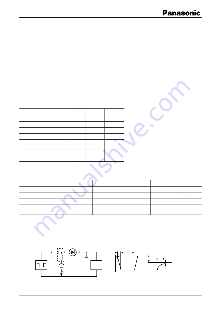
Bias Application Unit (N-50BU)
90%
Pulse Generator
(PG-10N)
R
s
=
50
Ω
Wave Form Analyzer
(SAS-8130)
R
i
=
50
Ω
t
p
=
2
µ
s
t
r
=
0.35 ns
δ =
0.05
I
F
=
100 mA
I
R
=
100 mA
R
L
=
100
Ω
10%
Input Pulse
Output Pulse
I
rr
=
0.1 I
R
t
r
t
p
t
rr
V
R
I
F
t
t
A
Note) *: The peak-to-peak value in one cycle of 50 Hz sine wave (non-repetitive)
Note) 1. Measuring methods are based on JAPANESE INDUSTRIAL STANDARD JIS C 7031 measuring methods for diodes.
2. This product is sensitive to electric shock (static electricity, etc.). Due attention must be paid on the charge of a human body
and the leakage of current from the operating equipment.
3. Absolute frequency of input and output is 1 GHz.
4. *: t
rr
measurement circuit
■
Package
•
Code
SMini2-F3
•
Pin Name
1: Anode
2: Cathode
■
Marking Symbol: 2B