
Switching Diodes
1
Publication date: October 2007
SKF00087AED
This product complies with the RoHS Directive (EU 2002/95/EC).
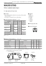
MA3S1370G
Silicon epitaxial planar type
For high-speed switching circuits
■
Features
•
Two isolated elements contained in one package, allowing high-
density mounting
•
Two diodes are connected in series in the package
■
Absolute Maximum Ratings
T
a
=
25
°
C
Parameter
Symbol
Conditions
Min
Typ
Max
Unit
Forward voltage
V
F
I
F
=
100 mA
1.2
V
Reverse voltage
V
R
I
R
=
100
µ
A
80
V
Reverse current
I
R
V
R
=
75 V
100
nA
Terminal capacitance
C
t
V
R
=
0 V, f
=
1 MHz
2
pF
Reverse recovery time
*
t
rr
I
F
=
10 mA, V
R
=
6 V
3
ns
I
rr
=
0.1 I
R
, R
L
=
100
Ω
■
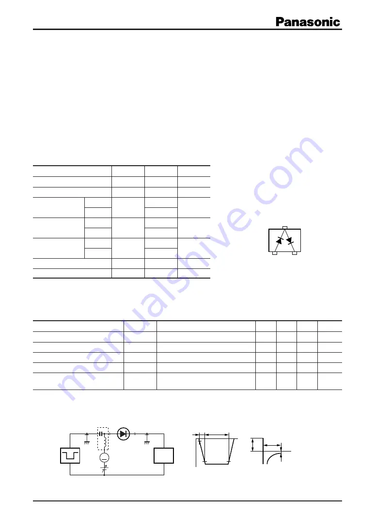
Electrical Characteristics
T
a
=
25
°
C
±
3
°
C
1
3
2
Bias Application Unit (N-50BU)
90%
Pulse Generator
(PG-10N)
R
s
=
50
Ω
Wave Form Analyzer
(SAS-8130)
R
i
=
50
Ω
t
p
=
2
µ
s
t
r
=
0.35 ns
δ =
0.05
I
F
=
10 mA
V
R
=
6 V
R
L
=
100
Ω
10%
Input Pulse
Output Pulse
I
rr
=
0.1 I
R
t
r
t
p
t
rr
V
R
I
F
t
t
A
Note) 1. Measuring methods are based on JAPANESE INDUSTRIAL STANDARD JIS C 7031 measuring methods for diodes.
2. Absolute frequency of input and output is 100 MHz.
3. *: t
rr
measurement circuit
Note) *: t
=
1 s
Parameter
Symbol
Rating
Unit
Reverse voltage
V
R
80
V
Maximum peak reverse voltage
V
RM
80
V
Forward current
Single
I
F
100
mA
Series
65
Peak forward
Single
I
FM
225
mA
current
Series
145
Non-repetitive peak
Single
I
FSM
500
mA
forward surge current
*
Series
325
Junction temperature
T
j
150
°
C
Storage temperature
T
stg
−
55 to
+
150
°
C
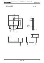
■
Package
•
Code
SSMini3-F3
•
Pin Name
1: Anode 1
2: Cathode 2
3: Cathode 1
Anode 2
■
Marking Symbol: MS
■
Internal Connection


