Schottky Barrier Diodes (SBD)
Publication date: October 2007
SKH00211AED
1
This product complies with the RoHS Directive (EU 2002/95/EC).
MA3SD29FG
Silicon epitaxial planar type
For super high speed switching circuits
Features
Low forward voltage V
F
:
<
0.42 V (at I
F
= 100 mA)
Optimum for high-frequency recti
fi
cation
Short reverse recovery time t
rr
Absolute Maximum Ratings
T
a
= 25
°
C
Parameter
Symbol
Rating
Unit
Reverse voltage
V
R
30
V
Repetitive peak reverse voltage
V
RRM
30
V
Forward current (Average)
Single
I
F(AV)
100
mA
Series
75
Peak forward current
Single
I
FM
200
mA
Series
150
Non-repetitive peak forward surge current
*
I
FSM
1
A
Junction temperature
T
j
125
°
C
Storage temperature
T
stg
–55 to +125
°
C
Note) *: 50 Hz sine wave 1 cycle (Non-repetitive peak current)
Electrical Characteristics
T
a
= 25
°
C
±
3
°
C
Parameter
Symbol
Conditions
Min
Typ
Max
Unit
Forward voltage
V
F1
I
F
= 10 mA
0.25
0.29
V
V
F2
I
F
= 100 mA
0.39
0.42
Reverse current
I
R1
V
R
= 10 V
25
m
A
I
R2
V
R
= 30 V
120
Terminal capacitance
C
t
V
R
= 0 V, f = 1 MHz
11
pF
Reverse recovery time
*
t
rr
I
F
= I
R
= 100 mA, I
rr
= 10 mA,
R
L
= 100
W
1
ns
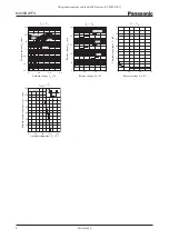
Note) 1. Measuring methods are based on JAPANESE INDUSTRIAL STANDARD JIS C 7031 measuring methods for diodes.
2. Absolute frequency of input and output is 250 MHz
3. This product is sensitive to electric shock (static electricity, etc.). Due attention must be paid on the charge of a human body and the leakage
of current from the operating equipment.
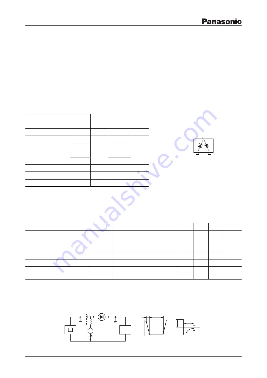
4. *: t
rr
measurement circuit
Bias Application Unit (N-50BU)
90%
Pulse Generator
(PG-10N)
R
s
=
50
Ω
Wave Form Analyzer
(SAS-8130)
R
i
=
50
Ω
t
p
=
2
µ
s
t
r
=
0.35 ns
δ =
0.05
I
F
=
I
R
=
100 mA
R
L
=
100
Ω
10%
Input Pulse
Output Pulse
I
rr
=
10 mA
t
r
t
p
t
rr
V
R
I
F
t
t
A
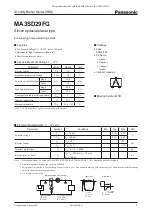
Package
Code
SSMini3-F3
Pin Name
1: Anode 1
2: Cathode 2
3: Cathode 1
Anode 2
Internal Connection
1
3
2
Marking Symbol: M5R


