background image

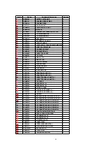
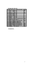
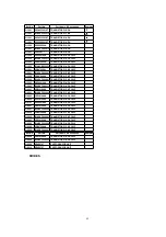
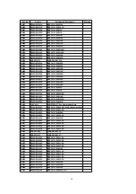
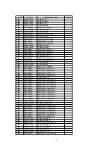
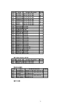
Ref. No.

Part No.

Part Name & Description

Remarks

C3518

ECJ2VF1C105Z

C CHIP 16V 1UF

C3519

ECJ2VB1H102K

C CHIP 50V 1000PF

C3520

ECJ2VF1C105Z

C CHIP 16V 1UF

C4001

ECJ2VF1C224Z

C CHIP 16V 0.22UF

C4002

ECEA1HKA010

ELECTROLYTIC 50V 1UF

C4003

ECJ2VB1H272K

C CHIP 50V 2700PF

C4004

ECJ2VB1H103K

C CHIP 50V 0.01UF

C4005

ECEA0JKA220

ELECTROLYTIC 6.3V 22UF

C4006

ECJ2VB1H102K

C CHIP 50V 1000PF

C4007

ECEA0JKA220

ELECTROLYTIC 6.3V 22UF

C4008

ECEA0JKA470

ELECTROLYTIC 6.3V 47UF

C4009

ECEA1CKA100

ELECTROLYTIC 16V 10UF

C4010

ECJ2VB1E273K

C CHIP 25V 0.027UF

C4011

ECJ2VB1H822K

C CHIP 50V 8200PF

C4012

ECEA1HKA010

ELECTROLYTIC 50V 1UF

C4013

ECEA1CKA100

ELECTROLYTIC 16V 10UF

C4014

ECEA1HKA010

ELECTROLYTIC 50V 1UF

C4017

ECJ2VB1H103K

C CHIP 50V 0.01UF ( B )

C4018

ECEA1HKA010

ELECTROLYTIC 50V 1UF ( A )

C4102

ECQB1562JF

POLYESTER 100V 5600PF

C4103

ECJ2VB1H103K

C CHIP 50V 0.01UF

C4104

ECJ2VB1H103K

C CHIP 50V 0.01UF

C4106

ECEA1CKS220I

ELECTROLYTIC 16V 22UF

C4151

ECEA1HKA010

ELECTROLYTIC 50V 1UF ( A )

C4152

ECEA1HKA010

ELECTROLYTIC 50V 1UF ( A )

C4153

ECEA1HKA010

ELECTROLYTIC 50V 1UF ( A )

C4154

ECEA1CKA101

ELECTROLYTIC 16V 100UF ( A )

C4155

ECJ2VF1E104Z

C CHIP 25V 0.1UF ( A )

C4201

ECEA1EKA4R7

ELECTROLYTIC 25V 4.7UF ( B )

C4202

ECEA1EKA4R7

ELECTROLYTIC 25V 4.7UF ( B )

C4203

ECEA0JKA330

ELECTROLYTIC 6.3V 33UF ( B )

C4204

ECEA0JKA330

ELECTROLYTIC 6.3V 33UF ( B )

C4205

ECEA1CKA100

ELECTROLYTIC 16V 10UF ( B )

C4206

ECEA1CKA100

ELECTROLYTIC 16V 10UF ( B )

C4207

ECEA1CKA100

ELECTROLYTIC 16V 10UF ( B )

C4208

ECEA1CKA100

ELECTROLYTIC 16V 10UF ( B )

C4209

ECEA1CKA100

ELECTROLYTIC 16V 10UF ( B )

C4210

ECEA1CKA100

ELECTROLYTIC 16V 10UF ( B )

C4211

ECJ2VB1H153K

C CHIP 50V 0.015UF ( B )

C4212

ECJ2VB1H153K

C CHIP 50V 0.015UF ( B )

C4213

ECEA1CKA100

ELECTROLYTIC 16V 10UF ( B )

C4214

ECEA1CKA101

ELECTROLYTIC 16V 100UF ( B )

C4216

ECEA1CKA100

ELECTROLYTIC 16V 10UF ( B )

C4217

ECEA0JKA220

ELECTROLYTIC 6.3V 22UF ( B )

C4218

ECEA1CKA100

ELECTROLYTIC 16V 10UF ( B )

C4219

ECEA1HKA010

ELECTROLYTIC 50V 1UF ( B )

C4227

ECJ2VF1C224Z

C CHIP 16V 0.22UF ( B )

C4229

ECJ2VF1H103Z

C CHIP 50V 0.01UF ( B )

C4230

ECEA0JKA470

ELECTROLYTIC 6.3V 47UF ( B )

C4451

ECJ2VB1H103K

C CHIP 50V 0.01UF ( B )

C4452

ECJ2VB1H103K

C CHIP 50V 0.01UF ( B )

C4455

ECJ2VB1E104K

C CHIP 25V 0.1UF ( B )

C4456

ECJ2VB1E104K

C CHIP 25V 0.1UF ( B )

C4459

ECEA0JKA101

ELECTROLYTIC 6.3V 100UF ( B )

69

Summary of Contents for NV-SJ4140PN

Page 1: ...deo Cassette Recorder NV SJ4140PN NV FJ6140PN SPECIFICATIONS 2003 Matsushita Electric Industrial Co Ltd All rights reserved Unauthorized copying and distribution is a violation of law 1 SAFETY PRECAUTIONS GENERAL GUIDELINES 1 ...

Page 2: ...3 When servicing observe the original lead dress If a short circuit is found replace all parts which have been overheated or damaged by the short circuit 4 After servicing see to it that all the protective devices such as insulation barriers insulation papers shields are properly installed 5 After servicing make the following leakage current checks to prevent the customer from being exposed to sho...

Page 3: ... of a shock hazard and the equipment should be repaired and rechecked before it is returned to the customer Figure 1 2 PREVENTION OF ELECTRO STATIC DISCHARGE ESD TO ELECTROSTATICALLY SENSITIVE ES DEVICES Some semiconductor solid state devices can be damaged easily by static electricity Such components commonly are called Electrostatically Sensitive ES Devices Examples of typical ES devices are int...

Page 4: ...r by conductive foam aluminum foil or comparable conductive material 7 Immediately before removing the protective material from the leads of a replacement ES device touch the protective material to the chassis or circuit assembly into which the device will be installed CAUTION Be sure no power is applied to the chassis or circuit and observe all other safety precautions 8 Minimize bodily motions w...

Page 5: ... will be displayed in F I P The Simplified Fault finding data is stored in the Memory IC IC6005 This data is cleared after it is displayed and then the POWER button is pressed back on 1 With power turned off press CH DOWN button on VCR for over 3 seconds if VCR is not in shut off condition Fig 1 1 2 Fault code 3 digit number will be displayed in F I P as shown Fig 1 2 Fig 1 3 5 ...

Page 6: ...Fig 1 4 Fig 1 5 6 ...

Page 7: ...a minute the VCR goes into VCR shut off condition Then the VCR stops and all VCR function buttons except for power become non operational 3 Lock data will be cleared at the first power on operation after lock code is displayed in FIP 4 1 2 USAGE SCREEN MODE Function displayed on the TV monitor the total elapsed Cylinder rotation time in hours 1 With power turned on and no cassette press CH DOWN bu...

Page 8: ... tape in this mode The VCR will return to normal operation mode 4 1 3 EEPROM IC IC6005 MAIN C B A REPLACEMENT NOTE After replacing EEPROM IC IC6005 or Main C B A be sure to perform the PG SHIFTER ADJUSTMENT in ELECTRICAL ADJUSTMENT procedures 4 1 4 SERVICE POSITION 4 1 4 1 Service Position CAUTION HOT CIRCUIT Primary circuit exists on the Main C B A Use extreme care to prevent accidental shock whe...

Page 9: ...4 1 4 1 2 Service Position 2 1 Normal Frame Model Fig 3 2 1 4 1 4 1 3 Service Position 2 2 Wide Frame Model Fig 3 2 2 9 ...

Page 10: ...correctly in Service Position 2 1 2 2 Recording can not be done In this case short the S Tab SW Pins on the foil side of the Main C B A to turn this SW on Fig 3 3 2 Place the tape between the Cassette Up Ass y and Main C B A to get a stability Fig 3 4 10 ...

Page 11: ... 4 1 The power comes on and the unit goes into service mode In this mode Mechanism movement can be confirmed When removing Cassette Up Ass y it can be confirmed without a cassette To release from this mode press POWER button off or disconnect AC Plug 4 1 7 TRACKING CENTER MODE TRACKING FIX AT CENTER Insert the Cassette tape Set the unit into Service Mode Turn on the power and play back the Cassett...

Page 12: ...l the Front Panel Ass y as follows 1 Swing the Cassette Door Lid all the way open until the Cassette Door tab clears the Opener Lever 2 Make sure that all locking tabs are aligned properly Then press the Front Panel straight in Fig 5 4 1 9 METHOD FOR LOADING UNLOADING OF MECHANISM 4 1 9 1 Manual Method Turn the Loading Gear clockwise for loading or counterclockwise for unloading using needlenose p...

Page 13: ... Portion b CAUTION Before applying DC Power Supply be sure to cut the Motor Leads with a cutter etc Otherwise the Loading Motor Drive IC IC2501 may be damaged Fig 6 2 4 1 9 2 1 WHEN LOADING WITHOUT A CASSETTE When loading without a cassette push Portion a on the Holder Unit of Cassette Up Ass y so that the Lever clear the First Tab and Second Tab Fig 6 3 13 ...

Page 14: ...ce Remove a jammed tape as follows 4 1 10 1 Manual Method When a tape jam is encountered check the tape loading condition and use the following procedure to remove a tape jam Fig 7 1 Method 1 1 Move the Pinch Roller Unit out by unhooking the Pin of Pinch Arm Unit so that the Pinch Roller is separated from the Capstan Rotor Unit shaft Fig 7 2 14 ...

Page 15: ... Up Ass y out far enough so that it clears the Drive Rack Arm slide the Drive Rack Unit as indicated by the arrow to remove the cassette tape from the Cassette Up Ass y 7 Check the cause of mechanical trouble and repair Fig 7 3 Method 2 1 Rotate Loading Motor counterclockwise with needlenose pliers etc so that the Pinch Roller is separated from the shaft of the Capstan Rotor Unit 2 Perform Step 2 ...

Page 16: ... Power Supply be sure to cut the Motor Leads with a cutter etc Otherwise the Loading Motor Drive IC IC2501 may be damaged 2 If loading does not start in approx 2 seconds after DC Power Supply is applied DO NOT continue to apply DC Power Supply Instead perform Manual Method 1 Be sure to cut the Motor Leads with a cutter etc 2 Apply 10 0 V DC Power Supply to the Loading Motor terminals 3 When the Lo...

Page 17: ...sed on the Mechanism Chassis to identify screws that require adjustment 4 1 13 HOW TO RESET ALL VCR MEMORY FUNCTIONS To reset clear the select language channel auto set and set clock functions to their initial power on condition power on no cassette inserted hold down the PLAY and CH UP buttons on the unit together for more than 5 seconds Power will shut off 4 1 14 HOW TO CONFIRM AUTO CLOCK SET FE...

Page 18: ...ll also protect VCR from being damaged by accidental shorting that may occur during servicing Also when troubleshooting the above type of Power Supply Circuit a variable isolation transformer is required in order to increase the input voltage slowly 4 1 16 SPECIAL NOTE All integrated circuits and many other semiconductor devices are electrostatically sensitive and therefore require the special han...

Page 19: ...Figure 19 ...

Page 20: ...over Install the Top Cover front portion at a downward angle so that the tab on the Front Panel Ass y fits into the hole in the Top Cover Then lower the rear portion into place and tighten 2 Screws 447 2 Installation of Front Panel Ass y CAUTION 20 ...

Page 21: ...perly Then press the Front Panel straight in Fig D1 3 Installation of Main C B A Mechanism Chassis onto the Frame When installing 2 Screws 460 slide the Holder Unit of the Cassette Up Ass y Refer to WHEN LOADING WITHOUT A CASSETTE in Service Notes to tighten screws Then slide it back to the EJECT Position 4 Installation of Mechanism Chassis and Cassette Up Ass y onto Main C B A A Make sure the Mod...

Page 22: ...4001 P6201 are aligned and seated securely 5 Connection of Mechanism Chassis Connect the Flat Cables Then install the A C Shield Plate as shown Fig D3 6 Installation of Cassette Up Ass y A Confirm that the Locking Tab under the Cassette Up Ass y is in Hole on the Mechanism Chassis when installing the Cassette Up Ass y Then slide the Cassette Up Ass y towards the back 22 ...

Page 23: ...HEN LOADING WITHOUT A CASSETTE in Service Notes to tighten screws Then slide it back to the EJECT Position C Hook Spring to the Drive Rack Arm on the Mechanism Chassis 5 2 MECHANISM SECTION 5 2 1 Disassembly Reassembly Method 5 2 2 Inner Parts Location Fig J1 1 23 ...

Page 24: ...5 2 3 EJECT Position Confirmation Fig J1 2 24 ...

Page 25: ...5 2 4 Full Erase Head and Cylinder Unit Fig J2 5 2 4 1 Reassembly Notes 1 After replacing the Cylinder Unit clear the Total elapsed Cylinder rotation time in hours to 0 Refer to USAGE SCREEN MODE in 25 ...

Page 26: ...gnment of Main Cam Gear Drive Rack Arm and Main Rod A Confirm that the hole on Main Rod is a Through Hole with a hole on chassis B Confirm that the hole on Drive Rack Arm is a Through Hole with a hole on chassis C Install the Main Cam Gear so that the projection of Main Cam Gear is in the upward position as shown Fig J3 2 26 ...

Page 27: ...ole with a hole on chassis B Confirm that the hole on Intermediate Gear A is aligned with the hole on Lift Gear Fig J3 3 C Install the Intermediate Gear B so that the hole on the Intermediate Gear B is aligned with the hole on the Main Cam Gear Fig J3 4 3 Holes on Main Cam Gear A The EJECT mode Hole on Main Cam Gear should be a Through 27 ...

Page 28: ...5 Installation of Main Cam Gear and Main Cam Push Nut A After installing the Support Angle install the Main Cam Push Nut with Needlenose Pliers etc so that it is flush with the chassis There may be some slight scratches on the Shaft of Main Cam Gear when removing the Main Cam Gear In case that the Main Cam Gear can be installed securely without tottering it is fine to use the one If any tottering ...

Page 29: ...5 2 6 1 Reassembly Notes 1 Installation of Center Clutch Unit A Fit the Center Clutch Unit into the Changing Gear Fig J4 2 5 2 7 Reel Gear Main Rod and SS Brake Arm Unit Fig J5 1 29 ...

Page 30: ...1 Alignment of Main Rod and T Loading Arm Unit A Align the Gear on T Loading Arm Unit with Gear of Main Rod Confirm that the Hole on Main Rod is a Through Hole with a hole on chassis Fig J5 2 5 2 8 Capstan Motor Unit Fig J6 30 ...

Page 31: ...g Arm Unit and S Loading Arm Unit A Install the S Loading Arm Unit onto the chassis B Install the T Loading Arm Unit so that the hole on T Loading Arm Unit is aligned with the hole on S Loading Arm Unit C Confirm that the holes on the S T Loading Arm Unit are Through Holes with hole on chassis Fig J7 2 31 ...

Page 32: ...5 2 10 T Brake Unit Tension Control Arm Unit T Reel Table S Reel Table and Tension Arm Unit Fig J8 1 5 2 10 1 Reassembly Notes 1 How to distinguish between S Reel Table and T Reel Table Fig J8 2 32 ...

Page 33: ...5 2 11 Loading Post Base T Unit and Loading Post Base S Unit Fig J9 5 2 12 Opener Piece Drive Rack Arm Pinch Arm Unit P5 Arm Unit and Intermediate Gear A Fig J10 1 33 ...

Page 34: ...e Gear A so that the hole on Intermediate Gear A is aligned with the hole on Lift Gear C Install the P5 Arm Unit so that it contacts with the tab of chassis Fig J10 2 2 Installation of Opener Piece A Install the Opener Piece so that the slot of the Opener Piece is inserted to the Pin of Pinch Arm Unit Fig J10 3 5 2 13 Motor Block Unit Audio Control Head Unit Lift Gear Tension Arm Boss and Cleaner ...

Page 35: ...5 3 CASSETTE UP ASSEMBLY SECTION 5 3 1 Top Plate Wiper Arm Unit and Holder Unit Fig K1 1 35 ...

Page 36: ... of Wiper Arm Unit and Drive Rack Unit A Slide the Drive Rack Unit to the far right as indicated by the arrow B Install the Wiper Arm Unit so that the hole on the Wiper Arm Unit is aligned with the hole on the Drive Rack Unit Fig K1 2 36 ...

Page 37: ...ve on Side Plate L and R B Insert Holder Unit boss A and B into the grooves as shown in Fig K1 1 C Finally in the EJECT Position confirm that the protrudence on the Wiper Arm Unit is aligned with the indentation on the Drive Rack Unit Fig K1 3 3 Make sure to hook the spring to the Drive Rack Arm of Mechanism chassis 37 ...

Page 38: ...2 1 CLEANING PROCEDURE FOR THE UPPER CYLINDER UNIT 1 While slowly turning the Upper Cylinder Unit counterclockwise by hand gently rub the Video Heads with a Head Cleaning Stick VFK27 moistened with Ethanol When using a Cleaning Cassette make sure to use DRY type only and be aware that excessive use can shorten head life Fig M1 38 ...

Page 39: ...othly with a constant tension Symptom of Misadjustment 1 If the tape tension is less than the specified value the tape cannot come into proper contact with the Video Heads resulting in poor picture playback 2 If the tape tension is too high the tape will soon be damaged Equipment Required Back Tension Meter Made in U S A Purchase Locally VHS Cassette Tape 120 Minute Tape Specification 22 4 gf 2 5 ...

Page 40: ... Control Arm Unit Fig M2 2 Note 1 Be sure that the three probes of the meter are all in solid contact with the tape but not touching any other parts of the mechanism 2 It is recommended that measurements should be repeated at least three 3 times because the tension meter is very sensitive to external vibrations 6 2 2 2 TAPE INTERCHANGEABILITY ADJUSTMENT Note To perform these adjustment confirmatio...

Page 41: ...e power comes on and the unit goes into service mode 3 Play back the alignment tape 4 To enter Tracking center mode press PLAY button in Play back mode TRACKING CENTER will be displayed on the TV monitor 5 Connect the oscilloscope to TP3002 on the Video Signal Process Section of the Main C B A Use TP6205 as a trigger 6 Confirm that the RF envelope is flat enough V1 V max is 0 7 or more If not with...

Page 42: ...lease from Tracking center mode press PLAY or STOP button 6 2 2 2 2 AUDIO CONTROL HEAD TILT ADJUSTMENT Purpose To confirm that the tape runs smoothly In particular confirm that the tape properly picks up the Audio Signal at the upper part of the head and the Control Signal at the lower part of the head Symptom of Misadjustment If the tilt of the Audio Control Head is poorly adjusted the tape will ...

Page 43: ...l Head replacement part is preset at the factory Purpose To be sure the tape runs properly along the Control Head Symptom of Misadjustment If the control signal is not properly picked up Servo Operation cannot be achieved A Blue screen will be seen in Playback This confirmation is required when the Audio Control Head is replaced 1 Play back a T120 cassette tape and check that the lower edge of the...

Page 44: ... the oscilloscope to the audio output jack on the rear side of the deck 2 Play back the 6 kHz Monaural Audio portion of the alignment tape 3 Adjust Black Screw C on the Audio Control Head base so that the output level is at maximum Fig M6 4 Confirm the height of the Audio Control Head is proper If not readjust Black Screws A and B 6 2 2 2 5 AUDIO CONTROL HEAD HORIZONTAL POSITION ADJUSTMENT Purpose...

Page 45: ... monitor 5 Connect the oscilloscope to TP3002 on the Video Signal Process Section of the Main C B A Use TP6205 as a trigger 6 Loosen the Black Screw D and tighten it slightly Set the H Position Adjustment Driver into the Hole A Then slowly turn the fixture either clockwise or counterclockwise so that the envelope is at maximum Fig M7 7 Tighten Black Screw D 8 To release from Tracking center mode p...

Page 46: ... Range 0 001 V to 50 V Div Frequency Range DC to 50 MHz Probes 10 1 1 1 2 Isolation Transformer Variable 3 VHS Alignment Tape VFMS0003H6 4 TV monitor 6 3 3 HOW TO READ THE ADJUSTMENT PROCEDURES Fig E1 6 3 4 PG SHIFTER ADJUSTMENT Purpose Determine the Video Head Switching Point during Playback Symptom of Misadjustment May cause Head Switching Noise and or Vertical Jitter Test Point TP3001 Main C B ...

Page 47: ...urn on the power and play back SP mode Then press 100 button on the remote to enter EVR PG SHIFTER ADJUSTMENT mode PG ADJUSTMENT screen will appear on the TV Monitor Fig E2 1 3 Connect the channel 1 scope probe to TP3001 and the channel 2 scope probe to TP6205 Used TP6205 as a trigger 4 Adjust value so that the trailing edge of the head switching pulse is placed 6 H 0 5 H 0 38 ms 0 03 ms before th...

Page 48: ...written to Memory IC IC6005 Fig E2 3 6 Press STOP button on the remote to release from EVR PG SHIFTER ADJUSTMENT MODE 6 4 TEST POINTS AND CONTROL LOCATION 7 SCHEMATIC DIAGRAMS 7 1 SCHEMATIC DIAGRAM CIRCUIT BOARD LAYOUT NOTES 7 2 MAIN SCHEMATIC DIAGRAMS 7 3 INTERCONNECTION SCHEMATIC DIAGRAM 7 4 VOLTAGE CHART 7 5 SIGNAL WAVEFORMS 48 ...

Page 49: ...8 CIRCUIT BOARD LAYOUT 8 1 MAIN C B A 9 BLOCK DIAGRAMS 9 1 OVERALL BLOCK DIAGRAM 10 EXPLODED VIEWS 10 1 MECHANISM TOP SECTION 49 ...

Page 50: ...10 2 MECHANISM BOTTOM SECTION 50 ...

Page 51: ...10 3 CASSETTE UP COMPARTMENT SECTION 51 ...

Page 52: ...10 4 CHASSIS FRAME AND CASING PARTS SECTION 52 ...

Page 53: ...10 5 PACKING PARTS AND ACCESSORIES SECTION 53 ...

Page 54: ...MENT PARTS LISTS BEFORE REPLACING PARTS READ THE FOLLOWING 11 1 REPLACEMENT NOTES 11 1 1 General Notes 1 Use only original replacement parts To maintain original function and reliability of repaired units use 54 ...

Page 55: ...arts list 5 Parts different in shape or size may be used However only interchangeable parts will be supplied as service replacement parts 6 Definition of Parts supplier A Parts with mark MKE in the Remarks column are supplied from MKE B Parts without mark in the Remarks column are supplied from MKI 7 Item numbers with capital letter E Example E10 E20 in the Ref No column are shown in the exploded ...

Page 56: ...s available separately as a replacement part 6 The Infrared Remote Control Unit Ref No 123 replacement part is available as a complete assembly unit only Do not try to disassemble the Infrared Remote Control Unit However the battery cover is available separately as a replacement part 7 Main Cam Push Nut Ref No 414 is not reusable If removed install a new one 11 1 3 Electrical Replacement Notes 1 U...

Page 57: ...t is available as a complete assembly unit only 5 EEP ROM IC IC6005 MAIN C B A replacement note After replacing EEP ROM IC IC6005 or MAIN C B A be sure to perform the PG SHIFTER ADJUSTMENT in ELECTRICAL ADJUSTMENT procedures 6 R6210 and C6202 replacement note Early units use a Main C B A with suffix version number LSJB2080 1 or LSJB2080 2 which employs two different methods as shown below When rep...

Page 58: ...0209 OPENER PIECE 1 8 LSVD0007 MAIN CAM GEAR KIT 2 9 LSDR0004 S REEL TABLE 1 10 LSDR0005 T REEL TABLE 1 11 LSEG0069 CYLINDER UNIT A 1 11 LSEG0070 CYLINDER UNIT B 1 12 LSEH0002 AUDIO CONTROL ERASE HEAD UNIT A 1 12 LSEH0004 AUDIO CONTROL ERASE HEAD UNIT B 1 13 K1MP06B00002 WIRE TRAP 6P A 1 13 K1MP09B00006 WIRE TRAP 9P B 1 14 LSDG0112 LIFT GEAR 1 16 VXDS0213 LOADING POST BASE S UNIT 1 17 VXDS0214 LOA...

Page 59: ...7152 FRONT PANEL ASS Y A 4 71 VYPS7153 FRONT PANEL ASS Y B 4 72 VYPS7128 CASSETTE DOOR LID UNIT A 4 72 VYPS7129 CASSETTE DOOR LID UNIT B 4 73 LSKM0766 TOP COVER 4 75 LSGP0244 REAR PANEL A 4 75 LSGP0243 REAR PANEL B 4 100 LSKF0322 BATTERY COVER 5 121 LSPG1508 PACKING CASE PAPER A 5 121 LSPG1509 PACKING CASE PAPER B 5 122 LSQF0702 FAN BAG 5 123 LSSQ0263 INFRARED REMOTE CONTROL UNIT A 5 123 LSSQ0264 ...

Page 60: ...G AC 120V 4 741 LSJA0361 AC CORD W PLUG AC 120V 4 743 ENG56D01G1F TUNER UHF VHF NR 4 771 EYF52BC FUSE HOLDER 4 E10 LSEP2080GC MAIN C B A A 4 RTL E10 LSEP2080HD MAIN C B A B 4 RTL SERVICE FIXTURES AND TOOLS Ref No Part No Part Name Description Remarks VFMS0003H6 VHS ALIGNMENT TAPE MKE VFKS0081 GREASE MKE VFK0329 POST ADJUSTMENT DRIVER MKE VFK27 HEAD CLEANING STICK MKE VFK0330 H POSITION ADJUSTMENT ...

Page 61: ... NN13400A IC LINEAR IC3101 MN3885S IC LINEAR IC4152 C1AB00001731 IC CMOS STANDARD LOGIC A E S D IC4201 AN3663FBP V IC LINEAR B IC6001 MN101D08EPB IC 8BIT MICROCONTROLLER E S D IC6002 B3NAA0000049 PHOTO INTERRUPUTER IC6003 B3NAA0000049 PHOTO INTERRUPUTER IC6004 C0EBJ0000080 IC CMOS STANDARD LOGIC E S D IC6004 C0EBJ0000099 IC CMOS STADNARD LOGIC E S D IC6004 RN5VS47CA TR IC CMOS STANDARD LOGIC E S D...

Page 62: ...P CHIP Q3003 2SD0601AHL TRANSISTOR SI NPN CHIP Q3003 B1ABCF000011 TRANSISTOR SI NPN CHIP Q4001 2SB1218AHL TRANSISTOR SI PNP CHIP Q4001 B1ADCF000063 TRANSISTOR SI PNP CHIP Q4002 2SD1819AHL TRANSISTOR SI NPN CHIP Q4003 2SD1819AHL TRANSISTOR SI NPN CHIP Q4101 2SD0601ARL TRANSISTOR SI NPN CHIP Q6001 2SD1819AHL TRANSISTOR SI NPN CHIP Q6001 B1ABCF000020 TRANSISTOR SI NPN CHIP Q6002 2SB0709AHL TRANSISTOR...

Page 63: ...1006 RGP15GL 5008 DIODE SI D1008 B0JAME000079 DIODE SI D1008 B0JAME000049 DIODE SI D1008 B0JANE000011 DIODE SI D1008 B0JANE000022 DIODE SI D1009 B0JCME000028 DIODE SI D1009 B0JCMD000006 DIODE SI D1009 B0JCMD000014 DIODE SI D1009 B0JCMD000018 DIODE SI D1009 MA2YD2300L DIODE SI D1009 SFPJ 53 DIODE SI D1015 MA2180LA DIODE ZENER 18V D1015 B0BA01800025 DIODE ZENER 18V D1015 1N4746A T DIODE ZENER 18V D1...

Page 64: ... ERDS2TJ104 CARBON 1 4W 100K R3001 ERJ6GEYJ750V MGF CHIP 1 10W 75 R3002 ERDS2TJ561 CARBON 1 4W 560 R3003 ERJ6GEYJ101V MGF CHIP 1 10W 100 R3004 ERJ6GEYJ750V MGF CHIP 1 10W 75 R3006 ERDS2TJ152 CARBON 1 4W 1 5K R3007 ERDS2TJ152 CARBON 1 4W 1 5K R3008 ERJ6GEYJ221V MGF CHIP 1 10W 220 R3009 ERJ6GEYJ221V MGF CHIP 1 10W 220 R3022 ERJ6GEYJ152V MGF CHIP 1 10W 1 5K R3023 ERJ6GEY0R00V MGF CHIP 1 10W 0 R3027 E...

Page 65: ...P 1 10W 8 2K B R4205 ERJ6GEYJ473V MGF CHIP 1 10W 47K B R4206 ERJ6GEYJ473V MGF CHIP 1 10W 47K B R4207 ERJ6GEYJ822V MGF CHIP 1 10W 8 2K B R4208 ERJ6GEYJ822V MGF CHIP 1 10W 8 2K B R4209 ERJ6GEYJ102V MGF CHIP 1 10W 1K B R4210 ERJ6GEYJ102V MGF CHIP 1 10W 1K B R4213 ERJ6GEYJ103V MGF CHIP 1 10W 10K B R4214 ERJ6GEYJ103V MGF CHIP 1 10W 10K B R4218 ERJ6GEYJ102V MGF CHIP 1 10W 1K B R4224 ERJ6GEYJ333V MGF CHI...

Page 66: ...102V MGF CHIP 1 10W 1K R6202 ERJ6GEYJ274V MGF CHIP 1 10W 270K R6203 ERJ6GEYJ103V MGF CHIP 1 10W 10K R6204 ERJ6GEYJ334V MGF CHIP 1 10W 330K R6205 ERJ6GEYJ473V MGF CHIP 1 10W 47K R6210 LSUC0015 RESISTOR KIT See Replacement Note R6210 ERJ6GEYJ825V MGF CHIP 1 10W 8 2M See Replacement Note R6228 ERJ6GEYJ122V MGF CHIP 1 10W 1 2K R6231 ERJ6GEYJ683V MGF CHIP 1 10W 68K R6232 ERJ6GEYJ682V MGF CHIP 1 10W 6 8...

Page 67: ...07 ECJ2VB1C224K C CHIP 16V 0 22UF C1009 VCYSBRE183KX CERAMIC 25V 0 018UF C1010 ECJ2VC1H101J C CHIP 50V 100PF C1011 ECA1HHG4R7I ELECTROLYTIC 50V 4 7UF C1012 ECEA1PEE331 ELECTROLYTIC 18V 330UF C1013 ECA1EM331B ELECTROLYTIC 25V 330UF C1016 ECEA1PEE331 ELECTROLYTIC 18V 330UF C1017 ECA0JM102B ELECTROLYTIC 6 3V 1000UF C1018 ECJ2VB1E104K C CHIP 25V 0 1UF C1019 ECA0JM471 ELECTROLYTIC 6 3V 470UF C1027 ECKA...

Page 68: ...IP 50V 56PF C3049 ECJ2VF1E104Z C CHIP 25V 0 1UF C3050 ECJ2VF1E104Z C CHIP 25V 0 1UF C3051 ECEA0JKA101 ELECTROLYTIC 6 3V 100UF C3052 ECJ2VF1H103Z C CHIP 50V 0 01UF C3053 ECEA1HKAR47 ELECTROLYTIC 50V 0 47UF C3054 ECEA1HKA2R2 ELECTROLYTIC 50V 2 2UF C3055 ECJ2VB1H392K C CHIP 50V 3900PF C3056 ECEA1HKA010 ELECTROLYTIC 50V 1UF C3062 ECJ2VF1E104Z C CHIP 25V 0 1UF C3101 ECEA1HKA010 ELECTROLYTIC 50V 1UF C31...

Page 69: ...UF A C4153 ECEA1HKA010 ELECTROLYTIC 50V 1UF A C4154 ECEA1CKA101 ELECTROLYTIC 16V 100UF A C4155 ECJ2VF1E104Z C CHIP 25V 0 1UF A C4201 ECEA1EKA4R7 ELECTROLYTIC 25V 4 7UF B C4202 ECEA1EKA4R7 ELECTROLYTIC 25V 4 7UF B C4203 ECEA0JKA330 ELECTROLYTIC 6 3V 33UF B C4204 ECEA0JKA330 ELECTROLYTIC 6 3V 33UF B C4205 ECEA1CKA100 ELECTROLYTIC 16V 10UF B C4206 ECEA1CKA100 ELECTROLYTIC 16V 10UF B C4207 ECEA1CKA100...

Page 70: ...J2VF1H103Z C CHIP 50V 0 01UF C6026 ECJ2VB1H102K C CHIP 50V 1000PF C6027 ECJ2VF1E104Z C CHIP 25V 0 1UF C6033 ECJ2VF1H104Z C CHIP 50V 0 1UF C6201 ECJ2VB1H332K C CHIP 50V 3300PF C6202 LSUC0015 RESISTOR KIT See Replacement Note C6202 ECKR1H102KB5 CERAMIC 50V 1000PF See Replacement Note C6203 ECJ2VB1H103K C CHIP 50V 0 01UF C6204 ECJ2VB1H103K C CHIP 50V 0 01UF C6217 ECJ2VF1E104Z C CHIP 25V 0 1UF C6218 E...

Page 71: ...SN101KA COIL 100UH L3506 ELESN101KA COIL 100UH L3507 ELESN101KA COIL 100UH L4001 ELELN153KA COIL 15MH L4002 ELESN101KA COIL 100UH L4101 ELESN471KA COIL 470UH L4201 ELESN101KA COIL 100UH B L4451 ELESN101KA COIL 100UH B L6201 ELEXT101KE04 COIL 100UH L6302 ELESN470KA COIL 47UH L7003 ELEXT101KE04 COIL 100UH CRYSTAL OSCILLATOR Ref No Part No Part Name Description Remarks X3010 H0D357400071 CRYSTAL OSCI...

Page 72: ... 1 6A PR1001 UNH000600A IC PROTECTOR 1 5A PR1001 B1ZAZ0000040 IC PROTECTOR 1 5A PR1001 LSSF009A25E IC PROTECTOR 1 5A PR1002 UNH000600A IC PROTECTOR 1 5A PR1002 B1ZAZ0000040 IC PROTECTOR 1 5A PR1002 LSSF009A25E IC PROTECTOR 1 5A TRANSFORMER Ref No Part No Part Name Description Remarks T1001 ETS28AD2J3AC SW TRANSFORMER T1001 LSTP0105 2 TRANSFORMER T1001 VTPS0042 SW TRANSFORMER T4101 EIQ7QF018Q OSC T...

Page 73: ...ISPLAY PANEL 741 LSJA0360 AC CORD W PLUG AC 120V 741 LSJA0348 AC CORD W PLUG AC 120V 741 LSJA0358 AC CORD W PLUG AC 120V 741 LSJA0359 AC CORD W PLUG AC 120V 741 LSJA0361 AC CORD W PLUG AC 120V 743 ENG56D01G1F TUNER UHF VHF NR 771 EYF52BC FUSE HOLDER 12 SCHEMATIC DIAGRAMS FOR PRINTING WITH LETTER SIZE 73 ...

Page 74: ...s counter part Use the interconnection schematic diagram to find the connection between associated connectors Example The connections between C B A s are shown below POWER SUPPLY C B A MAIN C B A The Number of pins of the Connector Connector No on Main C B A P1503 P3004 10 Pins Ref No of the connection parts such as lead cable flexible cable which is supplied as a replacement parts 244 3 Parts mar...

Page 75: ...05 WA30 J6100 WA30 J6003 PT IC6005 LSEQ0695 1 2 3 4 5 6 7 8 1 2 3 RESET IC6004 PST3147NR VSXS0232 TB X6001 RPI 303 IC6002 1 2 3 4 RPI 303 IC6003 1 2 3 4 P6201 K1KA12A00234 12 LODING MOTOR CONTROL REVERSE L STOP M REVERSE H 11 SIGNAL GND 10 VCC 14V FOR CYLINDER LODING MOTOR 9 CAPSTAN MOTOR SPEED CONTROL 8 CYLINDER SPEED CONTROL 7 CYLINDER PG FG OUTPUT 6 VCC 5V 5 CURRENT LIMIT FOR CAPSTAN MOTOR 4 VC...

Page 76: ...PHOTO_L S PHOTO_L TAKEUP PHOTO TR ON L SUPPLY PHOTO TR ON L DTS AFC TUNER AFC MTS_MODE MTS MODE POWER ON_L POWER ON L SW 27V ON H AT_ENV ENV VOLTAGE KEY4 KEY DATA 4 I KEY3 KEY DATA 3 I KEY2 KEY DATA 2 I KEY1 KEY DATA 1 I KEY11 KEY DATA 11 I I KEY10 KEY DATA 10 LED_H I J PLAY LED ON H SCAN1 SCAN2 SCAN 1 SCAN 2 POS 3 MODE SW POSITION C I POS 2 MODE SW POSITION B I I POS 1 MODE SW POSITION A ROT ROTA...

Page 77: ...00 16V C4154 1 50V C4153 0 1 C4155 WA5 L4151 PT R7004 PT C7024 3CH_HIZ 4CH_L SIF_IN 330 R4013 HIFI_MIX_OUT TV_L VCR_H 1000P C7010 UNSW_33V AFC 100U L7003 PT C7020 C4152 1 50V R4156 PT R4158 PT 1 50V C4151 R4160 PT 100 R4152 100K R4154 R4161 PT 100K R4153 100 R4151 R4157 PT R4159 PT R4155 PT Q4151 PT CMA_VIDEO Q3201 PT R3205 PT R3206 0 R3210 0 PT L3203 C3220 0 R3207 PT R3208 PT R3209 PT R3204 PT PT...

Page 78: ...NV DET REC PB D REC ON SP LP SLP SP LP SLP S VHS YNR ANR LIMITER HPF YNR MIX NON LINEAR DE EMPHASIS NON LINEAR EMPHASIS LIMITER HPF MAIN EMPHASIS COLOR KILLER SW W D CLIP CLAMP LPF DELAY OFF ON EE VV EE VV DOC SW CLAMP VV EE VV EE MAIN DE EMPHASIS Y C MIX GCA DET CLAMP LPF GCA MUTE Y C MIX CLAMP ARTFICIAL V H SYNC MIX EE VV ATT ATT ATT TUNER LINE 1 LINE 2 AGC DET SYNC SEPARATION I2C BUS VXO X2 BPF...

Page 79: ... WA5 J6301 WA5 J6315 PT J6356 WA5 J6311 WA5 J6303 WA5 J6360 WA5 J6310 PT J6316 WA5 J6313 PT J6312 WA5 J6308 WA5 J6358 WA5 J6314 PT J6305 PT J6302 WA5 J6357 PT SW6303 SW6302 CH_UP PLAY REC SW6312 W TYPE 01 B LED CH_UP SW6306 TV VCR FF SW6309 REW SW6301 W TYPE A LED CH_DOWN STOP EJECT POWER SW6315 REW SW6311 SW6307 POWER TV VCR SW6304 W LED 02 A MECA _SERVICE STOP EJECT REC SW6313 PLAY SW6308 CH_DOW...

Page 80: ...51 0 01 C4452 0 01 C4453 PT C4454 PT C4455 0 1 C4456 0 1 C4457 PT R4451 PT R4452 PT R4453 33K R4454 PT D4209 MA165 C4458 PT C4459 100 6 3V FL4901 PT 1 2 3 1500 R4455 PT TP4201 PT TP4202 TP4207 WA7 5 TP4204 PT D4202 PT 0 015 C4211 0 015 C4212 TP4208 PT C4917 0 1 C4918 0 1 C4919 0 1 C4920 0 022 C4921 PT R4456 PT 3R3 50V C4903 PT TP4205 1500 R4226 C4234 PT R4228 10K C4229 0 01 R4227 PT C4914 PT R4903...

Page 81: ...81 PT 2SD2159 Q1051 0 22 C1007 TP1006 PT TP1007 PT R1016 1K R1018 2200 C1018 0 1 R1015 2200 R1017 2430 R1014 220 LED_5V R1019 0 R1026 30 27V_ON_H UNSW_14V D1017 ERA15 01 30 R1025 C1081 PT C1060 10 16V Q1080 PT J1001 WA5 C1082 PT T1001 ETS28AD2J3 0N3131 R KT IC1001 1 2 3 4 IC1002 TA76431AS 2 3 1 F1001 1 6A 125V UNH000600A PR1002 UNH000600A PR1001 PR1080 PT J1008 PT J1002 WA7 5 J1009 0 J1007 PT 330 ...

Page 82: ...00P TP3801 PT SW_5V_VIDEO BLACK DET V LED_B CMA_AUDIO MA_AUDIO BLACK DET A LED_C E V MASK H_A_SW TP3807 PT C3830 0 056 0 47 50V C3826 R3823 PT R3824 PT R3825 PT R3826 PT R3827 PT R3828 PT AN3275 IC3801 1 2 3 4 5 6 7 8 9 10 27 28 29 30 31 32 33 34 35 36 19 20 21 22 23 24 25 26 11 12 13 14 15 16 17 18 13 15 34 20 14 2 16 10 8 5 6 33 4 17 26 27 12 9 3 36 31 28 30 1 22 32 11 23 25 24 19 18 29 35 21 7 ...

Page 83: ... MAIN C B A CN1 VIDEO OUT VIDEO IN 1 AUDIO OUT L CH AUDIO IN 1 L CH INFRARED RECEIVER UNIT TUNER UHF VHF UHF VHF IN UHF VHF OUT AUDIO OUT R CH AUDIO IN 1 R CH 17 Pins PIN PIN AC CORD 1 2 AC120V P3501 P3501 P4002 P4002 AUDIO CONTROL ERASE HEAD UNIT P4092 6 Pins VIDEO IN 2 AUDIO IN 2 L CH AUDIO IN 2 R CH MOTOR BLOCK UNIT PIN 2 Pins CYLINDER UNIT 9 Pins 6 Pins A B C D E F G H C D E F G H C D E F G H ...

Page 84: ...105 WA30 J6100 WA30 J6003 PT IC6005 LSEQ0695 1 2 3 4 5 6 7 8 1 2 3 RESET IC6004 PST3147NR VSXS0232 TB X6001 RPI 303 IC6002 1 2 3 4 RPI 303 IC6003 1 2 3 4 P6201 K1KA12A00234 12 LODING MOTOR CONTROL REVERSE L STOP M REVERSE H 11 SIGNAL GND 10 VCC 14V FOR CYLINDER LODING MOTOR 9 CAPSTAN MOTOR SPEED CONTROL 8 CYLINDER SPEED CONTROL 7 CYLINDER PG FG OUTPUT 6 VCC 5V 5 CURRENT LIMIT FOR CAPSTAN MOTOR 4 V...

Page 85: ...105 WA30 J6100 WA30 J6003 PT IC6005 LSEQ0695 1 2 3 4 5 6 7 8 1 2 3 RESET IC6004 PST3147NR VSXS0232 TB X6001 RPI 303 IC6002 1 2 3 4 RPI 303 IC6003 1 2 3 4 P6201 K1KA12A00234 12 LODING MOTOR CONTROL REVERSE L STOP M REVERSE H 11 SIGNAL GND 10 VCC 14V FOR CYLINDER LODING MOTOR 9 CAPSTAN MOTOR SPEED CONTROL 8 CYLINDER SPEED CONTROL 7 CYLINDER PG FG OUTPUT 6 VCC 5V 5 CURRENT LIMIT FOR CAPSTAN MOTOR 4 V...

Page 86: ... 50V C4153 0 1 C4155 WA5 L4151 PT R7004 PT C7024 3CH_HIZ 4CH_L SIF_IN 330 R4013 HIFI_MIX_OUT TV_L VCR_H 1000P C7010 UNSW_33V AFC 100U L7003 PT C7020 C4152 1 50V R4156 PT R4158 PT 1 50V C4151 R4160 PT 100 R4152 100K R4154 R4161 PT 100K R4153 100 R4151 R4157 PT R4159 PT R4155 PT Q4151 PT CMA_VIDEO Q3201 PT R3205 PT R3206 0 R3210 0 PT L3203 C3220 0 R3207 PT R3208 PT R3209 PT R3204 PT PT C3219 Q3202 P...

Page 87: ... 50V C4153 0 1 C4155 WA5 L4151 PT R7004 PT C7024 3CH_HIZ 4CH_L SIF_IN 330 R4013 HIFI_MIX_OUT TV_L VCR_H 1000P C7010 UNSW_33V AFC 100U L7003 PT C7020 C4152 1 50V R4156 PT R4158 PT 1 50V C4151 R4160 PT 100 R4152 100K R4154 R4161 PT 100K R4153 100 R4151 R4157 PT R4159 PT R4155 PT Q4151 PT CMA_VIDEO Q3201 PT R3205 PT R3206 0 R3210 0 PT L3203 C3220 0 R3207 PT R3208 PT R3209 PT R3204 PT PT C3219 Q3202 P...

Page 88: ...5 J6315 PT J6356 WA5 J6311 WA5 J6303 WA5 J6360 WA5 J6310 PT J6316 WA5 J6313 PT J6312 WA5 J6308 WA5 J6358 WA5 J6314 PT J6305 PT J6302 WA5 J6357 PT SW6303 SW6302 CH_UP PLAY REC SW6312 W TYPE 01 B LED CH_UP SW6306 TV VCR FF SW6309 REW SW6301 W TYPE A LED CH_DOWN STOP EJECT POWER SW6315 REW SW6311 SW6307 POWER TV VCR SW6304 W LED 02 A MECA _SERVICE STOP EJECT REC SW6313 PLAY SW6308 CH_DOWN SW6316 SW63...

Page 89: ...5 J6315 PT J6356 WA5 J6311 WA5 J6303 WA5 J6360 WA5 J6310 PT J6316 WA5 J6313 PT J6312 WA5 J6308 WA5 J6358 WA5 J6314 PT J6305 PT J6302 WA5 J6357 PT SW6303 SW6302 CH_UP PLAY REC SW6312 W TYPE 01 B LED CH_UP SW6306 TV VCR FF SW6309 REW SW6301 W TYPE A LED CH_DOWN STOP EJECT POWER SW6315 REW SW6311 SW6307 POWER TV VCR SW6304 W LED 02 A MECA _SERVICE STOP EJECT REC SW6313 PLAY SW6308 CH_DOWN SW6316 SW63...

Page 90: ...0 01 C4453 PT C4454 PT C4455 0 1 C4456 0 1 C4457 PT R4451 PT R4452 PT R4453 33K R4454 PT D4209 MA165 C4458 PT C4459 100 6 3V FL4901 PT 1 2 3 1500 R4455 PT TP4201 PT TP4202 TP4207 WA7 5 TP4204 PT D4202 PT 0 015 C4211 0 015 C4212 TP4208 PT C4917 0 1 C4918 0 1 C4919 0 1 C4920 0 022 C4921 PT R4456 PT 3R3 50V C4903 PT TP4205 1500 R4226 C4234 PT R4228 10K C4229 0 01 R4227 PT C4914 PT R4903 PT 1 2_OSC L4...

Page 91: ...0 01 C4453 PT C4454 PT C4455 0 1 C4456 0 1 C4457 PT R4451 PT R4452 PT R4453 33K R4454 PT D4209 MA165 C4458 PT C4459 100 6 3V FL4901 PT 1 2 3 1500 R4455 PT TP4201 PT TP4202 TP4207 WA7 5 TP4204 PT D4202 PT 0 015 C4211 0 015 C4212 TP4208 PT C4917 0 1 C4918 0 1 C4919 0 1 C4920 0 022 C4921 PT R4456 PT 3R3 50V C4903 PT TP4205 1500 R4226 C4234 PT R4228 10K C4229 0 01 R4227 PT C4914 PT R4903 PT 1 2_OSC L4...

Page 92: ... Q1051 0 22 C1007 TP1006 PT TP1007 PT R1016 1K R1018 2200 C1018 0 1 R1015 2200 R1017 2430 R1014 220 LED_5V R1019 0 R1026 30 27V_ON_H UNSW_14V D1017 ERA15 01 30 R1025 C1081 PT C1060 10 16V Q1080 PT J1001 WA5 C1082 PT T1001 ETS28AD2J3 0N3131 R KT IC1001 1 2 3 4 IC1002 TA76431AS 2 3 1 F1001 1 6A 125V UNH000600A PR1002 UNH000600A PR1001 PR1080 PT J1008 PT J1002 WA7 5 J1009 0 J1007 PT 330 25V C1013 2W ...

Page 93: ... Q1051 0 22 C1007 TP1006 PT TP1007 PT R1016 1K R1018 2200 C1018 0 1 R1015 2200 R1017 2430 R1014 220 LED_5V R1019 0 R1026 30 27V_ON_H UNSW_14V D1017 ERA15 01 30 R1025 C1081 PT C1060 10 16V Q1080 PT J1001 WA5 C1082 PT T1001 ETS28AD2J3 0N3131 R KT IC1001 1 2 3 4 IC1002 TA76431AS 2 3 1 F1001 1 6A 125V UNH000600A PR1002 UNH000600A PR1001 PR1080 PT J1008 PT J1002 WA7 5 J1009 0 J1007 PT 330 25V C1013 2W ...

Page 94: ...SW_5V_VIDEO BLACK DET V LED_B CMA_AUDIO MA_AUDIO BLACK DET A LED_C E V MASK H_A_SW TP3807 PT C3830 0 056 0 47 50V C3826 R3823 PT R3824 PT R3825 PT R3826 PT R3827 PT R3828 PT AN3275 IC3801 1 2 3 4 5 6 7 8 9 10 27 28 29 30 31 32 33 34 35 36 19 20 21 22 23 24 25 26 11 12 13 14 15 16 17 18 13 15 34 20 14 2 16 10 8 5 6 33 4 17 26 27 12 9 3 36 31 28 30 1 22 32 11 23 25 24 19 18 29 35 21 7 CMA_VIDEO COMM...

Page 95: ...SW_5V_VIDEO BLACK DET V LED_B CMA_AUDIO MA_AUDIO BLACK DET A LED_C E V MASK H_A_SW TP3807 PT C3830 0 056 0 47 50V C3826 R3823 PT R3824 PT R3825 PT R3826 PT R3827 PT R3828 PT AN3275 IC3801 1 2 3 4 5 6 7 8 9 10 27 28 29 30 31 32 33 34 35 36 19 20 21 22 23 24 25 26 11 12 13 14 15 16 17 18 13 15 34 20 14 2 16 10 8 5 6 33 4 17 26 27 12 9 3 36 31 28 30 1 22 32 11 23 25 24 19 18 29 35 21 7 CMA_VIDEO COMM...

Page 96: ...2 Pins MAIN C B A CN1 VIDEO OUT VIDEO IN 1 AUDIO OUT L CH AUDIO IN 1 L CH INFRARED RECEIVER UNIT TUNER UHF VHF UHF VHF IN UHF VHF OUT AUDIO OUT R CH AUDIO IN 1 R CH 17 Pins PIN PIN AC CORD 1 2 AC120V P3501 P3501 P4002 P4002 AUDIO CONTROL ERASE HEAD UNIT P4092 6 Pins VIDEO IN 2 AUDIO IN 2 L CH AUDIO IN 2 R CH MOTOR BLOCK UNIT PIN 2 Pins CYLINDER UNIT 9 Pins 6 Pins A B C D E F G H C D E F G H C D E ...

Page 97: ...2 Pins MAIN C B A CN1 VIDEO OUT VIDEO IN 1 AUDIO OUT L CH AUDIO IN 1 L CH INFRARED RECEIVER UNIT TUNER UHF VHF UHF VHF IN UHF VHF OUT AUDIO OUT R CH AUDIO IN 1 R CH 17 Pins PIN PIN AC CORD 1 2 AC120V P3501 P3501 P4002 P4002 AUDIO CONTROL ERASE HEAD UNIT P4092 6 Pins VIDEO IN 2 AUDIO IN 2 L CH AUDIO IN 2 R CH MOTOR BLOCK UNIT PIN 2 Pins CYLINDER UNIT 9 Pins 6 Pins A B C D E F G H C D E F G H C D E ...

Page 98: ...5 34 0 7 35 2 6 36 0 37 1 7 38 0 39 40 5 0 41 0 42 0 43 4 9 44 0 45 0 46 0 47 2 5 48 2 3 49 3 6 50 3 5 51 5 0 52 3 5 53 6 0 54 2 5 55 0 56 0 57 6 0 58 12 0 59 6 0 60 0 8 61 2 5 62 2 3 63 2 6 64 0 6 Q1001 E 0 C 173 0 B 0 3 Q1002 E 0 1 C 0 3 B 0 6 Q1051 E 11 9 C 15 0 B 12 4 Q1052 E 0 C 12 4 B 0 7 Q1053 E 5 2 C 5 3 B 5 9 Q3001 E 2 8 C 0 B 2 1 Q3002 E 2 7 C 0 B 2 0 Q3003 E 2 0 C 5 1 B 2 7 Q4001 E 5 1 ...

Page 99: ...3 8 3 7 30 0 0 31 5 0 5 0 32 5 0 5 1 33 2 7 2 7 34 2 6 2 6 35 2 6 2 7 36 5 1 5 1 37 2 4 2 4 38 2 4 2 6 39 0 0 40 5 1 5 1 41 5 2 5 3 42 0 1 0 2 43 44 45 0 0 46 47 2 1 2 1 48 0 0 49 2 0 2 1 50 2 7 2 8 51 5 2 5 3 52 1 3 2 7 53 2 6 2 7 54 5 0 5 0 55 1 5 0 4 56 0 0 57 58 59 60 61 62 63 64 0 0 65 1 4 1 4 66 5 1 5 1 67 2 4 0 8 68 0 0 69 1 0 2 6 70 2 6 2 6 71 0 0 72 2 6 2 6 73 5 1 2 2 74 3 0 2 6 75 2 2 1 ...

Page 100: ...Vp p V1 PIN 65 OF IC3001 0 2V 0 5ms1 REC PB WF12 52 0mVp p V1 PIN 55 OF IC3001 20mV 0 5ms1 PB WF13 V1 5 2Vp p PIN 93 OF IC3001 2V 2ms 1 CUE REV SLOW STILL WF14 0 24Vp p V1 PIN 31 OF IC3001 0 1V 5ms 2 REC WF15 0 35 Vp p V1 PIN 31 OF IC3001 0 2V 5ms 2 PB SP WF15 2 0Vp p V1 TP3001 1V 20µs1 REC PB WF16 0 24Vp p V1 CH1 TP3002 0 1V 5ms 2 REC CH2 TP6205 5V CH1 WF17 CH2 WF21 0 34Vp p V1 CH1 TP3002 0 1V 5m...

Page 101: ...CTOR 50V 2µs1 POWER ON WF26 10Vp p V1 PIN 5 OF T1001 5V 2µs1 POWER ON WF27 V1 PIN 8 OF T1001 10V 2µs1 POWER ON 40Vp p WF29 15 0Vp p V1 PIN 11 OF T1001 5V 2µs1 POWER ON WF30 0 23Vp p V1 BASE OF Q1002 0 1V 2µs1 POWER ON WF31 5 00Vp p V1 PIN 27 OF IC4201 2V 10ms1 PB WF32 0 44Vp p V1 PIN 53 OF IC4201 0 2V 0 5ms1 REC PB WF33 0 44Vp p V1 PIN 57 OF IC4201 0 2V 0 5ms1 REC PB WF34 0 44Vp p V1 PIN 59 OF IC4...

Page 102: ...ONTROL VIDEO LP SLP L HEAD VIDEO LP SLP R HEAD VIDEO SP R HEAD VIDEO SP L HEAD MODE SELECT SWITCH SW6002 P3501 PIN PIN PB AUDIO SIGNAL REC AUDIO SIGNAL PB VIDEO SIGNAL REC VIDEO SIGNAL VIDEO AUDIO VIDEO AUDIO VIDEO BLACK DET L SEGMENT a j GRID SEGMENT P4002 P4092 AUDIO HEAD AUDIO ERASE HEAD CONTROL HEAD PIN P4001 P6201 FULL ERASE HEAD Q6502 6505 6508 6510 5V RESET Q6001 6005 6006 IC6004 RESET IC60...

Page 103: ...H FIP VIDEO LP SLP L HEAD VIDEO LP SLP R HEAD Hi Fi AUDIO L HEAD Hi Fi AUDIO R HEAD VIDEO SP R HEAD VIDEO SP L HEAD I2C CONTROL MODE SELECT SWITCH SW6002 P3501 PIN PB AUDIO SIGNAL REC AUDIO SIGNAL PB VIDEO SIGNAL REC VIDEO SIGNAL VIDEO SIF VIDEO AUDIO L CH R CH VIDEO BLACK DET L P4002 P4092 AUDIO HEAD AUDIO ERASE HEAD CONTROL HEAD PIN P4001 FULL ERASE HEAD Q6502 6505 6508 6510 5V RESET Q6001 6005 ...

Page 104: ...15 C3211 C3210 C3220 C3017 C3218 C3207 C3203 C3217 R6203 TP6202 TP6201 TP6209 TP6101 TP6107 TP6208 TP6102 TP6005 TP6003 TP6018 TP6017 TP6019 TP6009 TP1002 TP6011 TP6010 TP6121 TP6103 TP6104 TP6105 TP6122 Q6001 IC6001 TP3004 TP3011 TP3102 IC3001 IC3101 TP3101 TP3401 Q3202 Q3201 Q3203 R1015 R1016 R1014 R1006 D1016 C1007 R1017 J1002 R1018 C1018 C1029 C1011 J1001 L1003 L1002 C1017 C1059 C1060 C1051 C1...

Reviews: