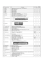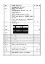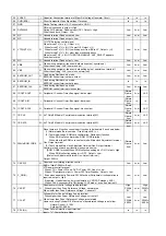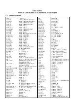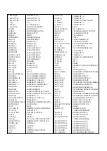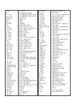
79 S.REEL.PULSE
I
Pulse Input terminal from reel sensor
In
In
In
80 T.REEL.PULSE
I
Pulse Input terminal from reel sensor
In
In
In
81 TUNER(H)
Video Input Selection Control Signal
Pin music secondary, Output = Low
UV/BS tuner CH selection : Output = High
Other than above : Output = Low
Low
Low
Low
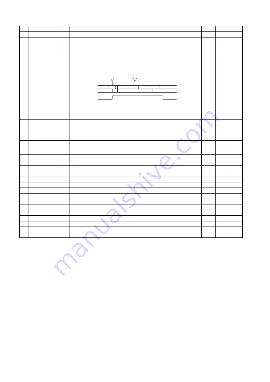
82 EX.FF/REW(L)
I/O
Control Signal Filter Selection Terminal during FF/REW
Control spec shall comply with Mecha FFREW(Hi-Z) output timing.
Set Input when deck enters FF/RRW mode.
During Stop, due to FF/REW stopping process, switch over to STOP3 first, then
STOP is canceled.
However, when starting FF/REW, Filter C addition will be required until it become
high speed. Then monitor the CTL Amp Gain(COH bit 0-2) setting value. When 5(
=60dB) or 7(=70dB), compulsorily, output = Low.
Low
Low
Low
83 UNLOADING(H)
I/O
Loading Motor Control terminal
shall comply with R4 mecha control spec.
Low
Low
Low
84 LOADING(H)
I/O
Loading Motor Control terminal
shall comply with R4 mecha control spec.
Low
Low
Low
85 S_VHS PB(H)
I
SVHS mode input
Input "H" = S - HVS
Input "L" = VHS
In
In
In
86 FG.AMP.OUT
O Capstan FG Amp Signal Output terminal.
Out
Out
Out
87 FG.AMP.IN
I
Capstan FG signal Input Terminal.
In
In
In
88 GND(A)
-
Analog GND.
-
-
-
89 VSS
Unused terminal. Connected to GND.
90 CYL.PFG
I
Cylinder P.FG signal Input Terminal.
In
In
In
91 OREF
O Analog Amp 1/2 Vdd Ref Power Output Terminal
Out
Out
Out
92 IREF
I
Analog Amp 1/2 Vdd Ref Power Input Terminal
In
In
In
93 VSS
Unused terminal. Connected to GND.
94 CTL.HEAD(-)
I/O Control head ( - )side Input/Output Terminal.
In/Out
In/Out
In/Out
95 CTL.HEAD(+)
I/O Control head ( + )side Input/Output Terminal.
In/Out
In/Out
In/Out
96 CTL.AMP.REF
I
Control Amp Ref Capacitor Connection Terminal
In
In
In
97 PB.CTL.OUT
O Control Amp Output terminal.
Out
Out
Out
98 5V(A)
-
Analog Amp Power Supply Terminal
-
-
-
99 5V(AD)
-
AD/8 bit DA Ref Power Supply Terminal.
-
-
-
100 VSS
Unused terminal.Connected to 5V.
STOP
FF/RE
W
STOP
STOP
21
00
00
26
28
00
PLA
Y
STO
P
FF/RE
W
27
Lo
w
Hi-Z
Deck
Position
PNO
EX.FF/REW(
Lo
w
Summary of Contents for NV-VP31GL
Page 7: ...7 ...
Page 8: ...8 ...
Page 30: ...7 REMOVAL OF THE POWER C B A Remove Screw D Fig D3 Remove 2 Screws P Fig D7 30 ...
Page 34: ...8 2 Traverse P C B 1 Unscrew the screws 2 Remove the solders 3 Remove the connectors 34 ...
Page 73: ...18 2 DVD MECHANISM CHASSIS PARTS SECTION 73 ...
Page 74: ...74 ...
Page 75: ...18 3 CASING PARTS SECTION 75 ...
Page 76: ...76 ...
Page 77: ...18 4 PACKING PARTS SECTION 77 ...
Page 88: ...C5004 ECJ1VB1H103K CHIP CAPACITOR 88 ...
Page 101: ...101 ...
Page 103: ...IC7551 PNA4618M12VT IR RECEIVER 103 ...
Page 137: ... VEP06F50A NV VP31GL GC GCS FRONT SW C B A 1 A B 2 3 4 5 ...
Page 138: ...NV VP31GL GC GCS FRONT JACK C B A VEP04849A 1 A B C 2 3 4 5 ...
Page 142: ... REP3406A 1N 1 A B C D E F 2 3 4 FOIL SIDE COMPONENT SIDE NV VP31GL GC GCS TRAVERSE C B A ...
Page 143: ......
Page 144: ......


