


1. Important safety notice
Components identified by the sign
have special
characteristics important for safety. When replacing any
of these components. Use only the specified parts.
2. Do not use the part number shown on this drawing for
ordering.
The correct part number and part value is shown in the
parts list, and may be slightly different or amended since
this drawing was prepared.
3. Use only original replacement parts:
To maintain original function and reliability of repaired
units, use only original replacement parts which are listed
with their part numbers in the parts list section of the
service manual.
4. Parts different in shape or size may be used.
However, only interchangeable parts will be supplied as
service replacement parts.
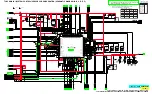
5. Test point information
: Test point with a jumper wire across a hole in P.C.B.
: Test point with no test pin.
:Test point with a component lead on the foil side.
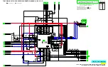
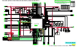
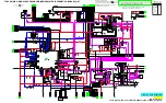
Schematic Diagram Notes
1. Indication for Zener Voltage of Zener Diodes
The Zener Voltage of Zener Diodes are indicated as such
on Schematic Diagrams.
Example:
(6.2V)......Zener Voltage
2. How to identify Connectors
Each connector is labeled with a Connector No. and Pin
No. Indicating what it is connected to,
in other words, its counter part.
Use the interconnection schematic diagram to find the
connection between associated connectors.
Example:
The connections between C.B.A.s are shown below.
POWER SUPPLY
C.B.A.
MAIN C.B.A.
The Number of pins of the Connector.
Connector No. on Main C.B.A.
P1503
P3004
(10 Pins)
Ref. No. of the connection parts such as lead cable,
flexible cable which is supplied as a replacement parts.
244
3. Parts marked "PT" are not used in any models included
in this service model.
Example:
100P
PT
C6011
R6097
PT
PT
C6014
4. Jumper wires are used for WA10, WA5 etc and these are
not supplied as replacement parts.
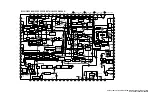
Signal Waveform Note
How to read Signal Waveform
Circuit Board Layout Note
Circuit Board Layout shows components installed for
various models.
For proper parts content for the model you are servicing,
please refer to the schematic diagram and parts list.
NOTE:
Circuit Board Layout includes components which are not
used.
Model No. Identification Mark
PVQ-1312W
PV-C1322-K
PV-C1352W-K
PVQ-2012
VV-2002
PV-C2022-K
PVQ-2512
PV-C2542
Not Used
A
B
C
D
E
F
G
H
PT
MODEL
MARK
COMPARISON CHART
OF MODELS & MARKS
9
1
2
3
4
5 6
7
WF1
8
+250mVp-p
V1
CH1 TP3002
0.1V
5ms 2
REC SP/LP/SLP
CH2 TP6205
5V
1
Connecting Point
2
Volts/Div
3
Volts/Div
4
Connecting Point
5
Time/Div
6
Trigger Channel of
the scope
(1:CH1,2:CH2)
7
Operation Mode of
VCR
8
Waveform Point on
Schematic
9
∆
V1:Peak to Peak
Note : Refer to item 3 of Schematic Diagram Notes for mark "PT".
Summary of Contents for Omnivision PV-C2542
Page 22: ...6 1 2 Disassembly Method Fig D2 22 ...
Page 23: ...Fig D3 23 ...
Page 24: ...6 1 2 1 Notes in chart 1 Removal of VCR Unit Fig D4 24 ...
Page 28: ...6 2 2 Inner Parts Location Fig J1 1 28 ...
Page 29: ...6 2 3 EJECT Position Confirmation Fig J1 2 29 ...
Page 30: ...6 2 4 Full Erase Head and Cylinder Unit Fig J2 30 ...
Page 70: ...70 ...
Page 73: ...11 2 MECHANISM BOTTOM SECTION 73 ...
Page 74: ...11 3 CASSETTE UP COMPARTMENT SECTION 74 ...
Page 75: ...11 4 CHASSIS FRAME SECTION 1 75 ...
Page 76: ...11 5 CHASSIS FRAME SECTION 2 76 ...
Page 77: ...11 6 PACKING PARTS AND ACCESSORIES SECTION 77 ...
Page 84: ...121 LSPG1279 PACKING CASE PAPER F 6 84 ...
Page 97: ...R5317 ERDS2TJ101 CARBON 1 4W 100 97 ...
Page 99: ...R6045 ERJ6GEYJ102V MGF CHIP 1 10W 1K 99 ...
Page 118: ...R5401 ERJ6GEYJ561V MGF CHIP 1 10W 560 118 ...