


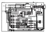


CHROMINANCE
SIGNAL PROCESS
MATRIX
OSD
CHARACTER
MIX/
BLANKING
LUMINANCE
SIGNAL PROCESS
I
2
C
CONTROL
BLANKING
BLUE AMP
GREEN AMP
RED AMP
Q351
Q352
Q353
RGB AMP
TP50
TP49
TP49
CRT
DISPLAY
CONTROL
Q3311
(TO/FROM IC6001(28))
I
2
C SERIAL DATA
(FROM IC6001(27))
I
2
C SERIAL CLOCK
BUFFER
VIDEO SIGNAL
Q3314
VERTICAL DEFLECTION
DRIVE
IC5301
(LUMINANCE/CHROMINANCE PROCESS)
IC3301
(CCV/OSD MICROCONTROLLER)
IC451
(VERTICAL DEFLECTION DRIVE)
Q431
Q571
Q501,Q551,T501, T502 HORIZONTAL
DRIVE
Q432,Q433,Q434
V POSITION
CONTROL
BUFFER
(FROM IC801(4))
+130V
OVER
CURRENT
DETECTOR
IC501,
Q581
VERTICAL
DEFLECTION
YOKE
HORIZONTAL
DEFLECTION
YOKE
FLYBACK
TRANS-
FORMER
ANODE
FOCUS
ABL
SCREEN
VIDEO+B
+B
HEATER
COLLECTOR
T551
HEATER
TP47
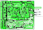
CRT C.B.A.
TV/VCR MAIN C.B.A.
TV PROCESS C.B.A.
VERTICAL C.B.A.
Q3315
B
G
R
VCO
3.58MHz OSC
25
31
3.58MHz
TO/FROM
PICTURE IN PICTURE
BLOCK DIAGRAM
CHROMINANCE
LUMINANCE
X5601
21
22
23
29 28 27 20
P351
4
P351
3
P5301
4
P5301
3
P5301
2
P351
2
P352
1
P352
3
P552
1
P552
3
D5304
43
44
16
18
11
33
40
10
19
TP3301
X3301
32KHz
36
41
5
6
14
5
6
15
19
20
21
22
32
18
17
OSD-R
OSD-G
OSD-B
VIDEO MUTE (H)
(FROM IC3101 (7))
VIDEO
(TO IC6001 (82))
OVER CURRENT (H)
(FROM Q801 (C))
DISCHARGE
OSD-BLANKING
12
7
4
2
2
4
6
1
V. PULSE
PROCESS
H. PULSE
PROCESS
COMPARATOR
NOT USED
NOT USED
4
BUFFER
FEED BACK
CIRCUIT
P452
4
P452
3
P452
2
P452
6
P452
5
PIN
15
PIN
14
PIN
13
PIN
17
P451
6
P451
3
P451
4
P451
5
PIN
4
PIN
1
PIN
2
PIN
3
P451
10
PIN
16
D503,C513
D502
+27V
DC
CONVERT
P451
9
P451
7
P451
1
P451
8
PIN
31
PIN
32
PIN
33
PIN
34
P5305
6
P5305
7
P5305
8
P5305
9
Q3310
PIN
37
PIN
36
P5305
12
P5305
11
PIN
17
PIN
5
PIN
28
PIN
6
PIN
3
PIN
4
PIN
5
PIN
10
PIN
9
PIN
7
PIN
8
PIN
1
P5302
4
PIN
30
P5305
5
PIN
6
P5302
6
P5302
1
P5302
2
P5302
3
P5303
11
P5302
5
P5305
3
D507
D544
D541
D506
Q502
Q541
Q542
DRIVE
BUFFER
Q5302
P8001
5
Summary of Contents for OmniVision PV-C2780-K
Page 8: ...Fig 1 3 Fig 1 4 8 ...
Page 26: ...Fig D5 6 1 2 1 Notes in chart 26 ...
Page 29: ...6 2 2 Inner Parts Location Fig J1 1 29 ...
Page 30: ...6 2 3 EJECT Position Confirmation Fig J1 2 30 ...
Page 31: ...6 2 4 Grounding Plate Unit Full Erase Head and Cylinder Unit Fig J2 1 31 ...
Page 44: ...6 3 CASSETTE UP ASS Y SECTION 6 3 1 Top Plate Wiper Arm Unit and Holder Unit Fig K1 1 44 ...
Page 81: ...81 ...
Page 85: ...11 2 MECHANISM BOTTOM SECTION 85 ...
Page 86: ...11 3 CASSETTE UP COMPARTMENT SECTION 86 ...
Page 87: ...11 4 CHASSIS FRAME SECTION 1 87 ...
Page 88: ...11 5 CHASSIS FRAME SECTION 2 88 ...
Page 89: ...11 6 PACKING PARTS AND ACCESSORIES SECTION 89 ...