background image

NOTE:

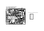
FOR SCHEMATIC DIAGRAM AND CIRCUIT BOARD LAYOUT NOTES,
REFER TO BEGINNING OF SCHEMATIC SECTION.

+1.000Vp-p

V1

PIN 20 OF IC3001

0.5V

20µs1

REC

 WF1

+1.000Vp-p

V1

PIN 16 OF IC3001

0.5V

20µs1

REC

 WF2

+0.410Vp-p

V1

PIN 29 OF IC3001

0.2V

20µs1

PB

 WF3

+0.590Vp-p

V1

PIN 27 OF IC3001

0.2V

20µs1

PB

 WF4

+190.0mVp-p

V1

PIN 46 OF IC3001

0.1V

5ms 1

PB

 WF5

+240mVp-p

V1

PIN 12 OF IC3001

0.1V

20µs1

REC

 WF6

+340mVp-p

V1

PIN 12 OF IC3001

0.1V

20µs1

PB

 WF6

+330mVp-p

V1

PIN 10 OF IC3001

0.1V

20µs1

REC

 WF7

+400mVp-p

V1

PIN 10 OF IC3001

0.1V

20µs1

PB

 WF7

+4.50Vp-p

V1

PIN 14 OF IC3001

2V

20µs1

REC/PB

 WF8

+100.0mVp-p

V1

PIN 71 OF IC3001

50mV

0.5ms1

REC

 WF9

+100.0mVp-p

V1

PIN 73 OF IC3001

50mV

0.5ms1

REC

 WF10

+2.60Vp-p

V1

PIN 65 OF IC3001

1V

0.5ms1

REC

 WF11

+1.20Vp-p

V1

PIN 69 OF IC3001

0.5V

0.5ms1

REC/PB

 WF12

+100.0mVp-p

V1

PIN 58 OF IC3001

50mV

0.5ms1

PB

 WF13

+1.20Vp-p

V1

TP4002

0.5V

0.5ms1

REC/PB

 WF14

V1  +5.00Vp-p

PIN 13 OF IC3001

2V

2ms 1

CUE/REV
/SLOW/STILL

 WF15

+0.180Vp-p

V1

PIN 34 OF IC3001

0.1V

5ms 2

PB

 WF16

+0.240Vp-p

V1

PIN 41 OF IC3001

0.2V

5ms 2

REC

 WF17

+0.350Vp-p

V1

PIN 41 OF IC3001

0.2V

5ms 2

PB  SP

 WF17

+1.000Vp-p

V1

TP3001

0.5V

20µs1

REC/PB

 WF18

+260mVp-p

V1

CH1 TP3002

0.1V

5ms 2

5V

REC

CH2 TP6205

 CH1 WF19
 CH2 WF34

+0.450Vp-p

V1

CH1 TP3002

0.2V

5ms 2

PB SP

CH2 TP6205

5V

 CH1 WF19
 CH2 WF34

+0.240Vp-p

V1

CH1 TP3002

0.2V

5ms 2

PB SLP

CH2 TP6205

5V

 CH1 WF19
 CH2 WF34

+1.000Vp-p

V1

PIN 15 OF IC3301

0.5V

20µs1

REC/PB

 WF20

+5.00Vp-p

V1

PIN 22 OF IC3301

2V

20µs1

STOP

 WF21
 (BLUE BACK)

+4.00Vp-p

V1

1V

5ms1

POWER ON

PIN10 OF IC5301

 WF23

+4.50Vp-p

V1

PIN 16 OF IC5301

5V

50µs1

POWER ON

 WF24

+1.30Vp-p

V1

PIN 18 OF IC5301

0.5V

20µs1

POWER ON

 WF25

+4.00Vp-p

V1

PIN 19 OF IC5301

1V

20µs1

POWER ON

 WF26

+4.20Vp-p

V1

PIN 21 OF IC5301

2V

20µs1

POWER ON

 WF27

+4.20Vp-p

V1

PIN 22 OF IC5301

2V

20µs1

POWER ON

 WF28

+5.00Vp-p

V1

PIN 23 OF IC5301

2V

20µs1

POWER ON

 WF29

+2.00Vp-p

V1

PIN 41 OF IC5301

1V

20µs1

POWER ON

 WF30

+2.500VDC

V1

TP6209

1V

5µs1

REC/PB

 WF31

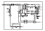
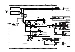
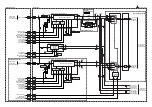
TV/VCR MAIN C.B.A. / TV PROCESS C.B.A. / VERTICAL C.B.A.

Summary of Contents for OmniVision PV-C2780-K

Page 1: ...03103C1 B6 Combination VCR PV C2780 PV C2780 K SPECIFICATIONS 2000 Matsushita Kotobuki Electronics Industries LTD All rights reserved Unauthorized copying and distribution is a violation of law 1 SAFETY PRECAUTIONS 1 ...

Page 2: ...ian from accidents resulting in personal injury from electrical shocks It will also protect Combination VCR from being damaged by accidental shorting that may occur during servicing 3 When servicing observe the original lead dress especially the lead dress in the high voltage circuits If a short circuit is found replace all parts which have been overheated or damaged by the short circuit 4 After s...

Page 3: ... jumper between the two prongs on the plug 2 For physically operated power switches turn power on Otherwise skip step 2 3 Measure the resistance value with an ohmmeter between the jumpered AC plug and each exposed metallic cabinet part on the receiver such as screwheads connectors etc When the exposed metallic part hasa return path to the chassis the reading should be between 1 M and 12 M When the...

Page 4: ...tential source of X Radiation in TV sets is the High Voltage section and the picture tube 2 When using a picture tube test fixture for service ensure that the fixture is capable of handling 32 0 kV without causing X Radiation NOTE It is important to use an accurate periodically calibrated high voltage meter 1 Reduce the brightness to minimum 2 Set the SERVICE switch to SERVICE 3 Measure the High V...

Page 5: ...s not present at that point when 120 V AC is applied find the cause Check R503 R5505 C5507 C513 and D503 3 Carefully check above specified parts and related circuits and parts When the circuit is repaired try the horizontal oscillator disable circuit test again CIRCUIT EXPLANATION HORIZONTAL OSCILLATOR DISABLE CIRCUIT The positive DC voltage supplied from the D503 cathode for monitoring high volta...

Page 6: ...ntial shock reasons prior to applying power to the unit under test 2 After removing an electrical assembly equipped with ES devices place the assembly on a conductive surface such as aluminum foil to prevent electrostatic charge buildup or exposure of the assembly 3 Use only a grounded tip soldering iron to solder or unsolder ES devices 4 Use only an antistatic solder removal device Some solder re...

Page 7: ...vides guidelines for proper grounding and in particular specifies that the cable ground shall be connectedto the grounding system of the building as close to the point of cable entry as practical 4 OPERATION GUIDE 5 SERVICE NOTES PLEASE READ 5 1 SERVICE NOTES 5 1 1 SIMPLIFIED FAULT FINDING DATA Simplified Self Diagnostic System facilitates finding the cause of the fault A 4 digit for fault code an...

Page 8: ...Fig 1 3 Fig 1 4 8 ...

Page 9: ...Fig 1 5 3 Press any operation button except for POWER on either the unit or the remote to detect that a key has been pressed The 1st digit changes to 0 only when key is detected Fig 1 6 9 ...

Page 10: ...wer become non operational 5 1 2 SERVICE POSITION 5 1 2 1 Service Position CAUTION HOT CIRCUIT Primary circuit exists on the TV VCR Main C B A and the TV Power C B A Use extreme care to prevent accidental shock when servicing 5 1 2 1 1 Service Position 1 Fig 2 1 5 1 2 1 2 Service Position 2 Fig 2 2 10 ...

Page 11: ...e TV Power C B A This circuit is identified as HOT on the C B A and in the Service Manual Use extreme care to prevent accidental shock when servicing 5 1 4 SERVICE MODE In order to inhibit detection of the Supply Takeup Photo Transistors Reel Sensor and Cylinder Lock place a jumper between TP6001 and GND In this mode Mechanism movement can be confirmed When removing Cassette Up Ass y it can be con...

Page 12: ...b clears the Opener Lever 2 Make sure that all guide tabs are aligned properly Then press the VCR Unit straight in Fig 3 5 1 6 HOW TO INITIALIZE MEMORY IC After the Memory IC IC6004 or TV VCR Main C B A is replaced be sure to set the Default value to Memory IC as shown in Memory IC Reference Table below 1 Press and hold STOP PLAY and VOL DOWN buttons on the unit together over 5 seconds with no cas...

Page 13: ...NTEREVR PG SHIFTER ADJUSTMENT MODE in ELECTRICAL ADJUSTMENT procedures Fig 4 2 3 Press and hold STOP PLAY and VOL DOWN buttons on the unit together over 5 seconds again or press the POWER button OFF to release EVR Adjustment Mode The Default value will be written to Memory IC IC6004 4 Perform all EVR Adjustments Refer to EVR Electronic Variable Register ADJUSTMENT WITH THE REMOTE CONTROL in ELECTR...

Page 14: ...G UNLOADING OF MECHANISM 5 1 7 1 Manual Method Turn the Loading Gear clockwise for loading or counterclockwise for unloading using needlenose pliers etc Note Do not use this method if Mechanism is jammed or locked Fig 5 1 14 ...

Page 15: ...ortion a DC to Portion b CAUTION Before applying DC Power Supply be sure to disconnect the Motor Leads from the Connector P2503 Otherwise the Loading Motor Drive IC IC2501 may be damaged Fig 5 2 When loading without a cassette push Portion a on the Holder Unit of Cassette Up Ass y so that the Lever clear the First Tab and Second Tab Fig 5 3 15 ...

Page 16: ...move a jammed tape as follows 5 1 8 1 Manual Method When a tape jam is encountered check the tape loading condition and use the following procedure to remove a tape jam Fig 6 1 5 1 8 1 1 Method 1 1 Move the Pinch Roller Unit out by unhooking the Pin of Pinch Arm Unit so that the Pinch Roller is separated from the Capstan Rotor Unit shaft Fig 6 2 16 ...

Page 17: ...e pulling the Cassette Up Ass y out far enough so that it clears the Drive Rack Arm slide the Drive Rack Unit as indicated by the arrow to remove the cassettetape from the Cassette Up Ass y 7 Check the cause of mechanical trouble and repair Fig 6 3 5 1 8 1 2 Method 2 1 Rotate Loading Motor counterclockwise with needlenose pliers etc so that the Pinch Roller is separated from the shaft of the Capst...

Page 18: ...d by rotating the Loading Gear CAUTION 1 Before applying DC Power Supply be sure to disconnect the Motor Leads from the Connector P2503 Otherwise the Loading Motor Drive IC IC2501 may be damaged 2 If loading does not start in approx 2 seconds after DC Power Supply is applied DO NOT continue to apply DC Power Supply Instead perform Manual Method 1 Be sure to disconnect the Motor Leads from the Conn...

Page 19: ...in C B A however it is possible to check the VCR even when CRT C B A and Anode Cap are removed 5 1 10 WIRE AND LEAD POSITION DIAGRAM Fig 8 5 1 11 DEFEATING THE AUTO TRACKING To defeat the Auto Tracking Function place the instrument in the STOP mode and place a jumper between TP6003 and TP6009 on the TV VCR Main C B A The tracking will be placed in the neutral position 19 ...

Page 20: ...sis is not isolated from the AC power line Use a transformer of adequate power rating as this protects the technician from accidentsresulting in personal injury from electrical shocks It will also protect Combination VCR from being damaged by accidental shorting that may occur during servicing Also when troubleshooting the above type of Power Supply Circuit a variable isolation transformer is requ...

Page 21: ...odes When the solder on both electrodes is melted remove the leadless component with a twisting motion Note A Do not attempt to lift the component off the board until the component is completely disconnected from the board by a twisting action B Be careful not to break the copper foil on the printed circuit board Fig 9 1 3 Installing the leadless component A Presolder the contact points on the cir...

Page 22: ...rcuit board 5 1 19 MODEL NO IDENTIFICATION MARK Use Marks shown in the chart below to distinguish the different models included in this Service Manual 5 2 IC TRANSISTOR AND CHIP PART INFORMATION 5 2 1 HOW TO READ THE IDENTIFICATION MARK OF CHIP COMPONENTS 22 ...

Page 23: ...APACITOR Because of the width of the color bands the reading direction cannot be specified However the color band can be read on either side Be sure to confirm the value using the schematic diagram CAUTION Once chip parts are removed they must not be reused Always use a new part when installing a chip part 6 DISASSEMBLY ASSEMBLY PROCEDURES 6 1 CABINET SECTION 6 1 1 Disassembly Flowchart Perform al...

Page 24: ...sassembly Method How to read chart shown above A Order of Procedure steps When reassembling perform steps s in reverse order These numbers are also used as the identification location No of parts in Figures 24 ...

Page 25: ...ig No showing Procedure or Part Location D Identification of part to be removed unhooked unlocked released unplugged or unsoldered 6 S 1 6 Screws S 1 6 L 1 6 Locking Tabs L 1 P 1 Spring P 1 E Refer to Notes in chart Fig D2 Fig D3 Fig D4 25 ...

Page 26: ...Fig D5 6 1 2 1 Notes in chart 26 ...

Page 27: ... Then press the VCR Unit straight in Fig D6 2 Removal of CRT Unit Place the Unit face down on a soft cloth before removing the CRT Unit 3 Installation of VCR Chassis Unit When installing 2 Screws S 6 slide the Holder Unit of the Cassette Up Ass y Refer to METHOD FOR LOADING UNLOADING OF MECHANISM in SERVICE NOTES totighten screws Then slide it back to the EJECT Position Make sure that Mechanism an...

Page 28: ...and Cassette Up Ass y straight onto the TV VCR Main C B A so that the Sensor LED clears the hole in the Mechanism Chassis and that 4 Connectors P6201 P6202 P3001 and P4001 are aligned and seated securely 5 Installation of Cassette Up Ass y A Confirm that the Locking Tab L 2 under the Cassette Up Ass y is in Hole on the Mechanism Chassis when installing the Cassette Up Ass y Then slide the Cassette...

Page 29: ...6 2 2 Inner Parts Location Fig J1 1 29 ...

Page 30: ...6 2 3 EJECT Position Confirmation Fig J1 2 30 ...

Page 31: ...6 2 4 Grounding Plate Unit Full Erase Head and Cylinder Unit Fig J2 1 31 ...

Page 32: ...is positioned on the front side of the Cylinder shaft so that the center line of the plateis just less than 1 0 mm measured from the center of the Cylinder shaft If required adjust the plate position by loosening Screw S 1 Never install the Grounding Plate Unit on the rear side of the Cylinder shaft Incorrect positioning will cause cylinder buzz Fig J2 2 32 ...

Page 33: ...6 2 5 Capstan Belt Support Angle Intermediate Gear B and Main Cam Gear Fig J3 1 6 2 5 1 Reassembly Notes 33 ...

Page 34: ...ection of Main Cam Gear is in the upward position as shown Fig J3 2 2 Confirmation Alignment of Intermediate Gear B Main Cam Gear and Intermediate Gear A A Confirm that the Hole A on Lift Gear is a Through Hole with a hole on chassis B Confirm that the hole on Intermediate Gear A is aligned with the hole on Lift Gear Fig J3 3 C Install the Intermediate Gear B so that the hole on the Intermediate G...

Page 35: ...onsists of a Main Cam Gear and a Main Cam Push Nut However Main Cam Push Nut is available separately as a replacement part 5 Installation of Main Cam Gear and Main Cam Push Nut A After installing the Support Angle install the Main Cam Push Nut with Needlenose Pliers etc so that it is flush with the chassis There may be some slight scratches on the Shaft of Main Cam Gear when removing the Main Cam ...

Page 36: ...able Install a new one 6 2 6 Center Clutch Unit Changing Gear Spring Changing Gear and Idler Arm Unit Fig J4 1 6 2 6 1 Reassembly Notes 1 Installation of Center Clutch Unit A Fit the Center Clutch Unit into the Changing Gear Fig J4 2 36 ...

Page 37: ... Fig J5 1 6 2 7 1 Reassembly Notes 1 Alignment of Main Rod and T Loading Arm Unit A Align the Gear of T Loading Arm Unit with Gear of Main Rod Confirm that the Hole on Main Rod is a Through Hole with a hole on chassis Fig J5 2 37 ...

Page 38: ...opper Angle Capstan Rotor Unit Oil Seal Capstan Stator C B A and MR Head Fig J6 1 6 2 8 1 Reassembly Notes 1 Application of Silicon Grease CAUTION When installing the IC2501 AN3845SC or Capstan Stator C B A 38 ...

Page 39: ... Rotor Unit and Oil Seal A Install the 2 Oil Seals into the Capstan Holder Unit Then insert the Capstan Rotor Unit Shaft into the hole of the Capstan Holder Unit so that shaft passes through 2 Oil Seals Be carefulnot to scratch the Shaft or Capstan Holder Unit B Align the bottom of Oil Seal A with notch line A Align the top of Oil Seal B with notch line B Fig J6 3 39 ...

Page 40: ...Loading Arm Unit onto the chassis B Install the T Loading Arm Unit so that the hole on T Loading Arm Unit is aligned with the hole on S Loading Arm Unit C Confirm that the holes on the S T Loading Arm Unit are Through Holes with hole on chassis Fig J7 2 6 2 10 T Brake Unit Tension Control Arm Unit T Reel Table S Reel Table and Tension Arm Unit Fig J8 1 40 ...

Page 41: ...ssist Spring or the Tension Arm Unit replace only the Tension Arm Unit with a new one and remove the Assist Spring 6 2 10 1 Reassembly Notes 1 How to distinguish between S Reel Table and T Reel Table Fig J8 2 6 2 11 Loading Post Base T Unit and Loading Post Base S Unit Fig J9 41 ...

Page 42: ...n Alignment of Intermediate Gear A Lift Gear and P5 Arm Unit A Rotate the Lift Gear so that Hole A on Lift Gear is a Through Hole with a hole on chassis B Install the Intermediate Gear A so that the hole on Intermediate Gear A is aligned with the hole on Lift Gear C Install the P5 Arm Unit so that it contacts with the tab of chassis 42 ...

Page 43: ...er Piece A Install the Opener Piece so that the slot of the Opener Piece is inserted to the Pin of Pinch Arm Unit Fig J10 3 6 2 13 Motor Block Unit Audio Control Head Unit Lift Gear Capstan Holder Unit and Tension Arm Boss Fig J11 43 ...

Page 44: ...6 3 CASSETTE UP ASS Y SECTION 6 3 1 Top Plate Wiper Arm Unit and Holder Unit Fig K1 1 44 ...

Page 45: ... of Wiper Arm Unit and Drive Rack Unit A Slide the Drive Rack Unit to the far right as indicated by the arrow B Install the Wiper Arm Unit so that the hole on the Wiper Arm Unit is aligned with the hole on the Drive Rack Unit Fig K1 2 45 ...

Page 46: ...ve on Side Plate L and R B Insert Holder Unit boss A and B into the grooves as shown in Fig K1 1 C Finally in the EJECTPosition confirm that the protrudence on the Wiper Arm Unit is aligned with the indentation on the Drive Rack Unit Fig K1 3 3 Make sure to hook the spring to the Drive Rack Arm of Mechanism chassis 46 ...

Page 47: ... 7 2 1 CLEANING PROCEDURE FOR THE UPPER CYLINDER UNIT 1 While slowly turning the Upper Cylinder Unit counterclockwise by hand gently rub the Video Heads with a Head Cleaning Stick VFK27 moistened with Ethanol When using a Cleaning Cassette make sure to use DRY type only and be aware that excessive use can shorten head life 47 ...

Page 48: ... runs smoothly with a constant tension Symptom of Misadjustment 1 If the tape tension is less than the specified value the tape cannot come into proper contact with the Video Heads resulting in poor picture playback 2 If the tape tension is too high the tape will soon be damaged Equipment Required Back Tension Meter Made in U S A Purchase Locally VHS Cassette Tape 120 Minute Tape Specification 20 ...

Page 49: ...he Tension Control Arm Unit Fig M2 2 Note A Be sure that the three probes of the meter are all in solid contact with the tape but not touching any other parts of the mechanism B It is recommended that measurements should be repeated at least three 3 times because the tension meter is very sensitive to external vibrations 7 2 2 2 MR HEAD GAP ADJUSTMENT Purpose To properly pick up the FG Signal Symp...

Page 50: ... the screwdriver clockwise until the MR Head touches the rotor Then turn it slightly counterclockwise to make theclearance as specified 4 Tighten Screw A 5 Reinstall the TV VCR Main C B A Fig M3 1 Note Do not touch the outside circumference of the rotor surface with any tool and keep magnetic material away from the rotor magnet especially metal particles Confirmation of Signal Level 1 Place the un...

Page 51: ...quipment Required Dual Trace Oscilloscope VHS Alignment Tape VFMS0003H6 Post Adjustment Driver VFK0329 H Position Adjustment Driver VFK0330 7 2 2 3 1 ENVELOPE OUTPUT ADJUSTMENT The height of the P2 and P3 Posts replacement part is preadjust at the factory Purpose To achieve a satisfactory picture and secure precise tracking Symptom of Misadjustment If the envelope is output poorly much noise will ...

Page 52: ...ht so that the envelope waveform becomes as flat V1 V max is 0 7 or more as possible No envelope drop If the envelope drop appears on the left half of the waveform adjust P2 post height If the envelope drop appears on the right half of the waveform adjust P3 post height CAUTION Overtightening P2 and P3 posts may cause the threads to strip Note It will be possible to confirm Step 5 according to fol...

Page 53: ...ged An intermittent Blue screen may be seen in Playback 1 Play back a T120 cassette tape and check that the tape travels smoothly between the upper and lower guides of the P4 post 2 If necessary adjust Black Screw B clockwise until the tape begins to curl at the lower edge of the P4 post Then adjust the screw counterclockwise until the curling is eliminated Fig M5 7 2 2 3 3 AUDIO CONTROL HEAD HEIG...

Page 54: ...or counterclockwise to raise Fig M6 7 2 2 3 4 AUDIO CONTROL HEAD AZIMUTH ADJUSTMENT Purpose To adjust the position and height of the Audio Control Head so that it meets the tape tracks properly Symptom of Misadjustment If the position of the Audio Control Head is not properly adjusted the Audio S N Ratio is poor 1 Connect the oscilloscope to the TP4002 on the TV VCR Main C B A 2 Play back the 6 kH...

Page 55: ...uit 1 Place a jumper between TP6003 and 5V TP6009 on the TV VCR Main C B A to defeat Auto Tracking 2 Eject the tape and insert it again to access the Neutral Tracking position 3 Play back the alignment tape 4 Connect the oscilloscope to TP3002 on the Video Signal Process Section of the TV VCR Main C B A Use TP6205 as a trigger 5 Loosen the Black Screw D and tighten it slightly Set the H Position A...

Page 56: ...nts the following equipment is required 1 Dual Trace Oscilloscope Voltage Range 0 001 V to 50 V Div Frequency Range DC to 50 MHz Probes 10 1 1 1 2 NTSC Video Pattern Generator 3 DVM Digital Volt Meter 4 MTS SAP Signal Generator TV Multi Channel Sound Modulator U S A 5 Frequency Counter Frequency Range 0 to 150 MHz 6 Plastic Tip Driver and Non Metal Driver 7 Isolation Transformer Variable 8 VHS Ali...

Page 57: ...tereo Signal will not be separated properly resulting in no stereophonic effect Test Point TP9001 TP9101 Audio C B A Adjustment R9001 R9008 R9101 R9108 Audio C B A Specification minimum level INPUT Antenna Input Terminal MTS ONLY L CH 300 Hz 5 Hz 3 kHz 5 Hz 14 or 7 Modulating Mode STEREO audio TV Equipment Oscilloscope MTS SAP Signal Generator 57 ...

Page 58: ... that the signal level of TP9001 is minimum 5 Set the MTS SAP Signal Generator as follows MTS ONLY L CH 3 kHz 5 Hz 14 or 7 Modulating 6 Adjust R9008 SEP H on the Audio C B A so that the signal level of TP9001 is minimum Fig E2 1 7 Set the MTS SAP Signal Generator as follows MTS ONLY L CH 300 Hz 5 Hz 14 or 7 Modulating 8 Connect the Oscilloscope to TP9101 on the Audio C B A 9 Adjust R9101 SEP L on ...

Page 59: ...RATION ADJUSTMENT are completed Purpose To separate the L and R Channels of Stereo Signal Symptom of Misadjustment The L and R Channels of Stereo Signal will not be separated properly resulting in no stereophonic effect Test Point TP9001 TP9101 Audio C B A Adjustment R9003 R9103 Audio C B A Specification minimum level INPUT Antenna Input Terminal MTS ONLY L CH 300 Hz 5 Hz 14 or 7 Modulating Mode S...

Page 60: ...ode and then set to STEREO audio 4 Adjust R9003 on the Audio C B A so that the signal level is minimum Fig E3 1 5 Connect the Oscilloscope to TP9101 on the Audio C B A 6 Adjust R9103 on the Audio C B A so that the signal level is minimum Fig E3 2 7 3 5 FM VCO ADJUSTMENT Purpose To set VCO free run frequency Symptom of Misadjustment Even when stereophony is received only monaural sound will be outp...

Page 61: ...201 on Audio C B A to GND through a resistor 3 3 k Then connect Frequency Counter to TP9201 Fig E4 2 3 Adjust R9206 FM VCO so that the frequency is 38 0 kHz 50 Hz 7 3 6 EVR Electronic Variable Register ADJUSTMENT WITH THE REMOTE CONTROL This unit has electronic technology using I2C Bus concept The following control functions are adjusted by using On Screen Displays and the remote control instead o...

Page 62: ...7 3 7 EVR ADJUSTMENT ITEM The following Items need to be adjusted for EVR adjustment PG SHIFTER ADJUSTMENT SUB CONTRAST ADJUSTMENT CUT OFF DRIVE ADJUSTMENT 62 ...

Page 63: ...djust 1 Press CH UP DOWN key on the remote control to select control function to be adjusted Important Note Make a note of the original value of the controls before modifying in case the wrong control is adjusted 2 Press VOL UP DOWN key on the remote control so that the shaded area moves to the value Fig E5 2 3 Press CH UP DOWN key on the remote control to adjust the value of the selected control ...

Page 64: ...again or press the POWER button OFF The adjusted value will be written to Memory IC IC6004 7 3 9 HOW TO ENTER EVR PG SHIFTER ADJUSTMENT MODE 1 Enter EVR adjustment mode 2 Insert the VHS Alignment Tape and playback in SP mode The adjustment overlay will appear Fig E5 6 7 3 9 1 How to adjust Press CH UP DOWN key on the remote control to adjust the value Fig E5 7 7 3 9 2 How to release from EVR PG Sh...

Page 65: ...de Press DISPLAY key again on the remote control 7 3 11 PG SHIFTER ADJUSTMENT Purpose Determine the Video Head Switching Point during Playback Symptom of Misadjustment May cause Head Switching Noise and or Vertical Jitter Test Point TP3001 TV VCR Main C B A TP6205 TV VCR Main C B A Adjustment PG SHIFTER EVR Specification T 6H 1H 0 38 ms 0 06 ms Input Mode SP Playback Equipment Oscilloscope VHS Ali...

Page 66: ...elease EVR PG Shifter Adjustment Mode The adjusted value will be written to Memory IC IC6004 Fig E6 7 3 12 SUB CONTRAST ADJUSTMENT Purpose To set the optimum sub contrast level Symptom of Misadjustment The picture is too dark or too light Test Point Pin 5 of P8001 TV PROCESS C B A or TP49 CRT C B A Adjustment SUB CONTRAST EVR R SUB CONTRAST EVR Specification 3 0 V p p 0 1 V p p Input Antenna Input...

Page 67: ...ote of the original value adjust to the D0 5 Select SUB CONTRAST in EVR adjustment mode and adjust so that the level A is 3 0 V p p 0 1 V p p 6 Select SUB BRIGHT in EVR adjustment mode and reset to the original value 7 Set PARENT PICTURE to UHF VHF TUNER TV DEMODULATOR 1 UNIT input 8 Select R SUB BRIGHT in EVR adjustment mode Then after making a note of the original value adjust to the D0 9 Select...

Page 68: ...ormer SUB BRIGHT EVR R SUB BRIGHT EVR B DRIVE EVR R DRIVE EVR B CUT OFF EVR G CUT OFF EVR R CUT OFF EVR Specification Refer to descriptions below Input Antenna Input Terminal Monoscope Pattern Signal Mode STOP Equipment Oscilloscope NTSC Video Pattern Generator 1 Set to PINP mode and then set PARENT PICTURE to UHF VHF TUNER TV DEMODULATOR 2 UNIT input 2 Supply a Monoscope Pattern Signal to the Ant...

Page 69: ...on the Flyback Transformer clockwise carefully and stop at the point where any color is first observed 10 In EVR adjustment mode select the two colors not observed in step 9 from the following control functions B CUT OFF G CUT OFF or R CUT OFF and adjust so that the horizontal line becomes white For example if the horizontal line appeared red in step 9 select and adjust the B CUT OFF and G CUT OFF...

Page 70: ...point where any color is first observed 21 In EVR adjustment mode select the two colors not observed in step 20 from the following control functions B CUT OFF G CUT OFF or R CUT OFF and adjust so that the horizontal line becomes white For example if the horizontal line appeared red in step 20 select and adjust the B CUT OFF and G CUT OFF 22 Press DISPLAY key on the remote control again to return f...

Page 71: ...Oscilloscope NTSC Video Pattern Generator 1 Set to PINP mode and then set PARENT PICTURE to UHF VHF TUNER TV DEMODULATOR 2 UNIT input 2 Supply the Rainbow Color Bar signal to Antenna Input Terminal 3 Select SUB BRIGHT in EVR adjustment mode Then after making a note of the original value adjust to the minimum C0 4 Connect the Oscilloscope to Pin 5 of P8001 on the TV PROCESS C B A or TP49 on the CRT...

Page 72: ... VHF TUNER TV DEMODULATOR 1 UNIT input 9 Select R SUB BRIGHT in EVR adjustment mode Then after making a note of the original value adjust to the minimum C0 10 Select R SUB TINT in EVR adjustment mode and adjust so that level A and B should be equal in amplitude 11 Select R SUB COLOR in EVR adjustment mode and adjust so that the level C is 1 50 V p p 0 15 V p p 7 3 15 V HEIGHT H POSITION ADJUSTMENT...

Page 73: ...l Mode STOP Equipment NTSC Video Pattern Generator 1 Supply a Monoscope Pattern Signal to the Video Input Jack 2 Select H CENTER in EVR adjustment mode and adjust so that A is approximately equal to width B 3 Select V SIZE in EVR adjustment mode and adjust so that the top 4th line is just in view 4 Confirm that the bottom 3rd line is in view and that the bottom 4th line is out of view If the line ...

Page 74: ...om of Misadjustment White becomes bluish or reddish Test Point TP50 CRT C B A Adjustment FOCUS CONTROL Flyback Transformer SCREEN CONTROL Flyback Transformer SUB BRIGHT EVR R SUB BRIGHT EVR G DRIVE EVR B DRIVE EVR R CUT OFF EVR G CUT OFF EVR B CUT OFF EVR Specification Refer to descriptions below Input 74 ...

Page 75: ...TP50 on the CRT C B A Use TP47 for GND 4 Select SUB BRIGHT and move the shaded area to the value in EVR adjustment mode 5 Adjust the FOCUS CONTROL on the Flyback Transformer so that the center of picture is the sharpest 6 Press DISPLAY key Service Switch on the remote control for collapse scan Refer toHOW TO ENTER SERVICE MODE 7 Turn the SCREEN CONTROL on Flyback Transformer fully counterclockwise...

Page 76: ...king a note of the original value adjust to the minimum C0 and while turning SUB BRIGHT value from minimum C0 up to maximum 3F confirm that the screenis tracking the White Pattern properly Repeat the above steps 6 10 12 and 13 until the screen is properly tracking the White Pattern 15 Set PARENT PICTURE to UHF VHF TUNER TV DEMODULATOR 1 UNIT input 16 Connect the Oscilloscope to TP50 on the CRT C B...

Page 77: ...t G DRIVE and B DRIVE in EVR adjustment mode and adjust so that the entire screen is white 27 Select R SUB BRIGHT in EVR adjustment mode Then after making a note of the original value adjust to the minimum C0 and while turning SUB BRIGHT value from minimum C0 up to maximum 3F confirm thatthe screen is tracking the White Pattern properly Repeat the above steps 19 23 25 and 26 until the screen is pr...

Page 78: ...ode and adjust so that the black screen starts to turn grey lighting only 7 3 18 PINP CHROMINANCE LEVEL ADJUSTMENT Purpose To set the optimum chrominance level Symptom of Misadjustment The CHILD PICTURE is too white or too black Test Point TP5312 TV PROCESS C B A Adjustment COLOR EVR Specification Refer to descriptions below Input Video Input Jack 100 chrominance signal Mode STOP Equipment NTSC Vi...

Page 79: ... on the TV PROCESS C B A 4 Select COLOR in EVR adjustment mode and adjust so that level A and B should be equal in amplitude Fig E12 1 Fig E12 2 7 3 19 PINP LUMINANCE LEVEL ADJUSTMENT Purpose To set the optimum luminance level Symptom of Misadjustment The CHILD PICTURE is too light or too dark Test Point TP5305 TV PROCESS C B A Adjustment PCONTRAST EVR Specification 79 ...

Page 80: ...INP mode and then move CHILD PICTURE to the upper left on monitor 2 Supply a Color Bar signal to the Video Input Jack 3 Connect the Oscilloscope to TP5305 on the TV PROCESS C B A 4 Select PCONTRAST in EVR adjustment mode and adjust so that level A and B should be equal in amplitude Fig E13 1 Fig E13 2 7 4 TEST POINTS AND CONTROL LOCATION 80 ...

Page 81: ...81 ...

Page 82: ...GRAM AND CIRCUIT BOARD LAYOUT NOTES 8 2 MAIN I SYSTEM CONTROL SERVO OPERATION CYLINDER DRIVE SCHEMATIC DIAGRAM 8 3 MAIN II SIGNAL PROCESS OSD AUDIO SCHEMATIC DIAGRAM 8 4 MAIN III SCHEMATIC DIAGRAM 8 5 MAIN IV AUDIO AMP SCHEMATIC DIAGRAM 82 ...

Page 83: ...D AMP SCHEMATIC DIAGRAM 8 15 CRT SCHEMATIC DIAGRAM 8 16 CAPSTAN STATOR SCHEMATIC DIAGRAM 8 17 INTERCONNECTION SCHEMATIC DIAGRAM 8 18 SIGNAL WAVEFORM 8 19 VOLTAGE CHART 9 CIRCUIT BOARD LAYOUT 9 1 TV VCR MAIN C B A 9 2 AUDIO C B A 9 3 TV PROCESS C B A 9 4 VERTICAL C B A TV POWER C B A CAPSTAN STATOR C B A 9 5 Hi Fi AUDIO VIDEO HEAD AMP C B A CRT C B A 10 BLOCK DIAGRAMS 10 1 POWER SUPPLY BLOCK DIAGRA...

Page 84: ...i AUDIO SIGNAL PATH BLOCK DIAGRAM 10 6 SYSTEM CONTROL BLOCK DIAGRAM 10 7 SERVO BLOCK DIAGRAM 10 8 PICTURE IN PICTURE BLOCK DIAGRAM 10 9 TV YC PROCESS BLOCK DIAGRAM 11 EXPLODED VIEWS 11 1 MECHANISM TOP SECTION 84 ...

Page 85: ...11 2 MECHANISM BOTTOM SECTION 85 ...

Page 86: ...11 3 CASSETTE UP COMPARTMENT SECTION 86 ...

Page 87: ...11 4 CHASSIS FRAME SECTION 1 87 ...

Page 88: ...11 5 CHASSIS FRAME SECTION 2 88 ...

Page 89: ...11 6 PACKING PARTS AND ACCESSORIES SECTION 89 ...

Page 90: ...12 REPLACEMENT PARTS LISTS BEFORE REPLACING PARTS READ THE FOLLOWING 12 1 REPLACEMENT NOTES 12 1 1 General Notes 1 Use only original replacement parts 90 ...

Page 91: ...rs of replacement parts according to the parts list 5 Parts different in shape or size may be used However only interchangeable parts will be supplied as service replacement parts 6 Parts with mark MKA in Remarks column are supplied from MKA Others are supplied from MKE 12 1 2 Mechanical Replacement Notes 1 Section No of parts shown in Exploded Views are indicated in the Remarks column 2 Main Cam ...

Page 92: ...1 000 M 1 000 k All capacitors are in F P F 10 All coils are in H M 1 000 H 10 4 Abbreviation RTL Retention Time Limited This indicates that the retention time is limited for this item After the discontinuation of this item in production it will no longer be available NR Non Repairable Board Ass y MGF CHIP Metal Glaze Film Chip C CHIP Ceramic Chip COMPLX CMP Complex Component W FLMPRF Wirewound Fl...

Page 93: ... UHF VHF TUNER TV DEMODULATOR UNIT 1 Ref No E21 and the UHF VHF TUNER TV DEMODULATOR UNIT 2 Ref No E150 have already been pre adjusted at the factory donot try to adjust them Their replacement parts are available as a complete assembly unit only 10 Since the FM TRANSMITTER C B A Ref No E139 has already been pre adjusted at the factory do not try to adjust the FM TRANSMITTER C B A The FM TRANSMITTE...

Page 94: ...CLUTCH UNIT 2 42 VMBS1151 CHANGING GEAR SPRING 2 43 LSDG0114 CHANGING GEAR 2 44 VXLS1091 IDLER ARM UNIT 2 45 VXPS0391 CAPSTAN ROTOR UNIT 2 46 LSMA0387 STOPPER ANGLE 2 47 LSMM0002 MAIN ROD 2 48 LXQVB01270 COLOR PICTURE TUBE UNIT 4 MKA 49 VXLS1099 S LOADING ARM UNIT 2 50 VXLS1098 T LOADING ARM UNIT 2 51 LSDG0116 REEL GEAR 2 52 LSDG0111 INTERMEDIATE GEAR B 2 53 LSMA0423 SUPPORT ANGLE 2 54 LSDV0007 CA...

Page 95: ...MX0143 SUPPORT PIECE 5 MKA 258 KL 250 19 PURSE LOCK CLAMPER 4 MKA 12 2 2 SCREWS AND WASHERS Ref No Part No Part Name Description Remarks 401 VHDS0475 SCREW STEEL 1 405 VHDS0496 SCREW W WASHER STEEL 5 410 VHDS0498 SCREW W WASHER STEEL 1 414 VHNS0070 MAIN CAM PUSH NUT STEEL 2 422 XWGV2D5G WASHER NYLON 2 424 XYC26 SF6J SCREW W WASHER STEEL 1 426 TMM77532 CUSHION RUBBER 4 430 XTV26 6FFZJ TAPPING SCREW...

Page 96: ...CR MAIN C B A INTEGRATED CIRCUITS Ref No Part No Part Name Description Remarks IC501 TLP621GR IC LINEAR OVER CURRENT DETECTOR MKA IC1001 0N3131 R KT IC LINEAR ERROR V DET IC2601 AN3808K IC LINEAR CYLINDER MOTOR DRIVE IC3001 AN3479FBP A IC LINEAR VIDEO AUDIO PROCESS IC3101 NJM2235M IC BIPOLAR LINEAR VIDEO INPUT SW IC3201 MN3885S IC CCD 1H DELAY E S D IC3301 LC8632165N41 IC 8BIT MICROCONTROLLER E S ...

Page 97: ... 2SD601 R S CHIP Q1053 2SD2097TV2R CHIP Q1057 2SA1175 TF MKA OR 2SA1175 TH MKA OR 2SA1175 TJ MKA OR 2SA1175 TK MKA OR 2SA564A Q R S OR 2SA733 TK MKA OR 2SA733 TP MKA OR 2SA733 TQ MKA Q1058 2SC2412K1 CHIP OR 2SD601 R S CHIP Q3001 2SA1037K146R CHIP OR 2SB709A CHIP Q3002 2SC2412K1 CHIP OR 2SD601A CHIP Q3310 2SC2412K1 CHIP OR 2SD601A CHIP Q3311 2SA1037K146R CHIP OR 2SB709A CHIP Q3314 HN1C01F GR COMPLX...

Page 98: ...146R CHIP OR 2SB709A CHIP Q6003 2SC2412K1 CHIP OR 2SD601A CHIP Q6004 2SA1037K146R CHIP OR 2SB709A CHIP Q6005 2SC2412K1 CHIP OR 2SD601A CHIP Q6006 DTA143EK CHIP OR UN211L CHIP Q6007 2SC2412K1 CHIP OR 2SD601A CHIP Q6009 VEKS5707 PHOTO SENSOR UNIT Q6010 VEKS5707 PHOTO SENSOR UNIT Q6301 2SC2412K1 CHIP OR 2SD601A CHIP Q6302 2SC2412K1 CHIP OR 2SD601A CHIP Q6303 2SC2412K1 CHIP OR 2SD601A CHIP Q7001 2SA10...

Page 99: ...GE ABSORBER 360 MKA D882 ERZV10V361CS SURGE ABSORBER 360 MKA D1001 S1WBA60B D1002 ERA18 04V3 D1003 ERA18 04V3 D1005 ERA18 04V3 D1006 ERC30 01L3 OR RU3YXLFC1 D1007 ERA18 04V3 D1008 ERC81 004 D1011 MA4051N TAKT ZENER 5 1V D1012 MA858 OR 1SS135T 77 D1013 MA165 OR 1SS119 OR 1SS133T D1015 MA7180 ZENER 18V D1016 MA165 OR 1SS119 OR 1SS133T D1051 MA4100N ZENER 10V OR RD10JSAB3 ZENER 10V D1052 MA165 OR 1SS...

Page 100: ...VCYSARH101KB CERAMIC 50V 100P D4703 VCYSARH101KB CERAMIC 50V 100P D4705 VCYSARH101KB CERAMIC 50V 100P D4708 MA111 CHIP D4710 MA111 CHIP D6001 VEKS5708 SENSOR LED UNIT D6002 MA165 OR 1SS119 OR 1SS133T D6003 MA165 OR 1SS119 OR 1SS133T D6201 MA165 OR 1SS119 OR 1SS133T D6202 MA165 OR 1SS119 OR 1SS133T D6301 SLP913C81HAB LED RED D6302 SLP313C81HAB LED GREEN D6303 SLP413C81HAB LED ORANGE MKA RESISTORS 1...

Page 101: ...2TJ473 47K R586 ERDS2TJ393 39K R591 ERF5ZJ121 W FLMPRF 5W 120 R809 ERJ6GEYJ222V MGF CHIP 1 10W 2 2K R810 ERDS2TJ101 100 R811 ERDS2TJ103 10K R812 VRESC2TK825T SOLID 10 1 2W 8 2M R815 ERDS2TJ223 22K R1003 VRESE2TJ334 1 2W 330K R1004 ERG2SJ333H METAL OXIDE 2W 33K R1005 ERG1SJ680P METAL OXIDE 1W 68 R1006 ERJ6GEYJ222V MGF CHIP 1 10W 2 2K R1007 ERDS2TJ101 100 R1008 ERDS2TJ392 3 9K R1010 ERD25FJ100P 10 O...

Page 102: ... ERJ6GEYJ474V MGF CHIP 1 10W 470K R3028 ERJ6GEYJ272V MGF CHIP 1 10W 2 7K R3029 ERJ6GEYJ151V MGF CHIP 1 10W 150 R3032 ERJ6GEYJ122V MGF CHIP 1 10W 1 2K R3035 ERJ6GEYJ103V MGF CHIP 1 10W 10K R3036 ERJ6GEYG102V MGF CHIP 2 1 10W 1K R3037 ERJ6GEYG102V MGF CHIP 2 1 10W 1K R3038 ERJ6GEYJ222V MGF CHIP 1 10W 2 2K R3077 ERJ6GEYJ101V MGF CHIP 1 10W 100 R3081 ERJ6GEYJ103V MGF CHIP 1 10W 10K R3082 ERJ6GEYJ223V ...

Page 103: ...0W 10K R3390 ERJ6GEYJ222V MGF CHIP 1 10W 2 2K R4001 ERJ6GEYJ103V MGF CHIP 1 10W 10K R4002 ERJ6GEYJ334V MGF CHIP 1 10W 330K R4003 ERJ6GEYJ221V MGF CHIP 1 10W 220 R4004 ERJ6GEYJ333V MGF CHIP 1 10W 33K R4005 ERJ6GEYJ225V MGF CHIP 1 10W 2 2M R4006 ERJ6GEYJ681V MGF CHIP 1 10W 680 R4007 ERJ6GEYJ821V MGF CHIP 1 10W 820 R4008 ERJ6GEYJ273V MGF CHIP 1 10W 27K R4009 ERJ6GEYJ473V MGF CHIP 1 10W 47K R4010 ERJ6...

Page 104: ...ERJ6GEYJ222V MGF CHIP 1 10W 2 2K R6007 ERJ6GEYJ221V MGF CHIP 1 10W 220 R6008 ERJ6GEYJ221V MGF CHIP 1 10W 220 R6011 ERJ6GEYJ102V MGF CHIP 1 10W 1K R6012 ERJ6GEYJ102V MGF CHIP 1 10W 1K R6013 ERJ6GEYJ102V MGF CHIP 1 10W 1K R6022 ERJ6GEY0R00V MGF CHIP 1 10W 0 R6024 ERJ6GEYJ221V MGF CHIP 1 10W 220 R6025 ERJ6GEYJ221V MGF CHIP 1 10W 220 R6026 ERJ6GEYJ103V MGF CHIP 1 10W 10K R6027 ERJ6GEYJ101V MGF CHIP 1 ...

Page 105: ...24 ERJ6GEYJ475V MGF CHIP 1 10W 4 7M R6125 ERJ6GEYJ332V MGF CHIP 1 10W 3 3K R6126 ERJ6GEYJ182V MGF CHIP 1 10W 1 8K R6127 ERJ6GEYJ563V MGF CHIP 1 10W 56K R6128 ERDS2TJ221 220 R6129 ERDS2TJ221 220 R6130 ERJ6GEYJ103V MGF CHIP 1 10W 10K R6150 ERJ6GEYJ472V MGF CHIP 1 10W 4 7K R6151 ERJ6GEYJ472V MGF CHIP 1 10W 4 7K R6152 ERJ6GEYJ472V MGF CHIP 1 10W 4 7K R6159 ERJ6GEYJ563V MGF CHIP 1 10W 56K R6161 ERJ6GEY...

Page 106: ...2V MGF CHIP 1 10W 1K R6508 ERDS2TJ102 1K R6509 ERDS2TJ102 1K R6511 ERDS2TJ102 1K R6512 ERJ6GEYJ102V MGF CHIP 1 10W 1K R6513 ERJ6GEYJ102V MGF CHIP 1 10W 1K R6514 ERDS2TJ102 1K R6515 ERDS2TJ103 10K R6516 ERDS2TJ103 10K R6517 ERDS2TJ103 10K R6518 ERJ6GEYJ103V MGF CHIP 1 10W 10K R6522 ERJ6GEYJ101V MGF CHIP 1 10W 100 R6523 ERJ6GEYJ101V MGF CHIP 1 10W 100 R6524 ERDS2TJ102 1K R6525 ERDS2TJ102 1K R6526 ER...

Page 107: ...iption Remarks C501 ECQB1H473KM POLYESTER 50V 0 047 MKA C510 ECKW2H681KB5 CERAMIC 500V 680P C513 ECA1HM100B ELECTROLYTIC 50V 10 C524 ECKC3D471KBP CERAMIC 2KV 470P C531 ECA1HM3R3B ELECTROLYTIC 50V 3 3 MKA C552 ECA1EM471E ELECTROLYTIC 25V 470 C553 ECKW2H221KB5 CERAMIC 500V 220P C554 ECWH12H682JS POLYESTER 5 1200V 6800P C556 ECWF2564JBP POLYESTER 5 250V 0 64 OR ECWF2564JSB POLYESTER 5 250V 0 64 C558 ...

Page 108: ...ECA0JM102B ELECTROLYTIC 6 3V 1000 C1018 ECUV1E104ZFN C CHIP 80 20 25V 0 1 C1021 EEUGA1H1R0B ELECTROLYTIC 50V 1 C1025 VCKSFKK102MX CERAMIC 20 125V 1000P OR VCKSFMK102MX CERAMIC 20 125V 1000P OR VCKSFVK102MX CERAMIC 20 125V 1000P C1028 ECEA1PEE331 ELECTROLYTIC 18V 330 C1030 VCYSBRE183KX CERAMIC 25V 0 018 C1051 ECEA1HKAR47 ELECTROLYTIC 50V 0 47 C1052 ECEA1CKA100 ELECTROLYTIC 16V 10 C1058 ECEA0JEE101 ...

Page 109: ...C3038 ECEA1CKA100 ELECTROLYTIC 16V 10 C3041 ECUV1H103ZFN C CHIP 80 20 50V 0 01 C3043 ECUV1H392KBN C CHIP 50V 3900P C3044 ECUV1H103ZFN C CHIP 80 20 50V 0 01 C3045 ECEA1HKAR47 ELECTROLYTIC 50V 0 47 C3046 ECEA1HKA2R2 ELECTROLYTIC 50V 2 2 C3047 ECEA0JKA221 ELECTROLYTIC 6 3V 220 C3048 ECUV1E104ZFN C CHIP 80 20 25V 0 1 C3050 ECEA1HKA2R2 ELECTROLYTIC 50V 2 2 C3054 ECUV1H103ZFN C CHIP 80 20 50V 0 01 C3055...

Page 110: ...5V 0 033 C4011 ECUV1H103KBN C CHIP 50V 0 01 C4012 ECEA1HKA010 ELECTROLYTIC 50V 1 C4013 ECEA0JKA470 ELECTROLYTIC 6 3V 47 C4014 ECEA1HKA010 ELECTROLYTIC 50V 1 C4051 ECUV1E333KBN C CHIP 25V 0 033 C4102 ECQB1562JF POLYESTER 5 100V 5600P C4103 ECUV1H103KBN C CHIP 50V 0 01 C4104 ECUV1H103KBN C CHIP 50V 0 01 C4105 ECEA1CKA220 ELECTROLYTIC 16V 22 C4171 ECEA1HKA010 ELECTROLYTIC 50V 1 C4502 ECEA1CKA100 ELEC...

Page 111: ...CUV1H680JCN C CHIP 5 50V 68P C6208 ECUV1E104KBN C CHIP 25V 0 1 C6209 ECUV1E104ZFN C CHIP 80 20 25V 0 1 C6211 ECEA0JKS470 ELECTROLYTIC 6 3V 47 C6212 ECUV1H100CCN C CHIP 0 25P 50V 10P C6213 ECUV1H272KBN C CHIP 50V 2700P C6214 ECUV1H102KBN C CHIP 50V 1000P C6218 ECEA0JKS101 ELECTROLYTIC 6 3V 100 C6219 ECEA1EKS4R7 ELECTROLYTIC 25V 4 7 C6220 ECUV1H103KBN C CHIP 50V 0 01 C6223 ECUV1E104KBN C CHIP 25V 0 ...

Page 112: ... L4004 VLQSH02R100K 10 L4101 ELESN471KA 470 L4701 ELEXT101KE04 100 L4702 ERJ6GEY0R00V MGF CHIP 1 10W 0 L4703 BK2125HM102 FERRITE CORE 1K L4704 ERJ6GEY0R00V MGF CHIP 1 10W 0 L6002 ELEXT101KE04 100 L7002 VLQSAB7D100K 10 L7101 VLQSAB7D100K 10 CRYSTAL OSCILLATOR Ref No Part No Part Name Description Remarks X3001 VSXS0195 X3301 VSXS0238 MKA X6001 VSXS0784 MKA X6501 EF0GC4004T4 PIN HEADERS Ref No Part N...

Page 113: ...E 125V 1 6A OR XBA1C16NU100 FUSE 125V 1 6A PR1001 ICP N38 TP1 IC PROTECTOR 1 5A OR UNH000600A IC PROTECTOR 1 5A PR1003 ICP F25 1 IC PROTECTOR 1 0A MKA OR UN11010 IC PROTECTOR 1 0A MKA PR1004 ICP F25 1 IC PROTECTOR 1 0A MKA OR UN11010 IC PROTECTOR 1 0A MKA PR1005 ICP F25 1 IC PROTECTOR 1 0A MKA OR UN11010 IC PROTECTOR 1 0A MKA RELAY Ref No Part No Part Name Description Remarks RL801 TSEH0005 RELAY ...

Page 114: ... VSCS1072 HEAT SINK E138 XYN3 F8S SCREW W WASHER STEEL E147 LSMB0226 FM ANTENNA MKA E148 LSGF0037 BARRIER MKA E150 ENG36704G TUNER 2 UHF VHF NR E151 T3A1301 GROUNDING STRAP E152 VEKS5755 GROUNDING WIRE MKA E153 LSZC0001 SHEET CU MKA 12 3 2 AUDIO C B A INTEGRATED CIRCUITS Ref No Part No Part Name Description Remarks IC4201 AN3962FB V IC LINEAR Hi Fi AUDIO PROCESS IC4271 UPC4574G2 T1 IC LINEAR OP AM...

Page 115: ...1V MGF CHIP 1 10W 510 R4204 ERJ6GEYJ511V MGF CHIP 1 10W 510 R4205 ERDS2TJ393 39K R4206 ERJ6GEYJ393V MGF CHIP 1 10W 39K R4207 ERJ6GEYJ183V MGF CHIP 1 10W 18K R4208 ERJ6GEYJ183V MGF CHIP 1 10W 18K R4209 ERJ6GEY0R00V MGF CHIP 1 10W 0 R4210 ERA6YEB153V MGF CHIP 0 1 1 10W 15K R4211 ERJ6GEYJ152V MGF CHIP 1 10W1 5K R4212 ERJ6GEYJ152V MGF CHIP 1 10W 1 5K R4213 ERJ6GEYJ123V MGF CHIP 1 10W 12K R4214 ERJ6GEY...

Page 116: ...01 ELESN101KA 100 R4302 ELESN101KA 100 R4303 ERDS2TJ333 33K R4304 ERJ6GEYJ333V MGF CHIP 1 10W 33K R4305 ERJ6GEYJ223V MGF CHIP 1 10W 22K R4306 ERJ6GEYJ223V MGF CHIP 1 10W 22K R4307 ERJ6GEYJ183V MGF CHIP 1 10W 18K R4308 ERJ6GEYJ183V MGF CHIP 1 10W 18K R4309 ERJ6GEYJ103V MGF CHIP 1 10W 10K R4310 ERJ6GEYJ103V MGF CHIP 1 10W 10K R4311 ERJ6GEY0R00V MGF CHIP 1 10W 0 R4312 ERJ6GEY0R00V MGF CHIP 1 10W 0 R9...

Page 117: ... 10W 33K R9114 ERJ6GEYJ223V MGF CHIP 1 10W 22K R9115 ERJ6GEYJ333V MGF CHIP 1 10W 33K R9116 ERJ6GEYJ223V MGF CHIP 1 10W 22K R9117 ERJ6GEYJ821V MGF CHIP 1 10W 820 R9118 ERJ6GEYJ102V MGF CHIP 1 10W 1K R9201 ERJ6GEYJ102V MGF CHIP 1 10W 1K R9202 ERDS2TJ103 10K R9203 ERJ6GEYJ102V MGF CHIP 1 10W 1K R9204 ERJ6GEYJ224V MGF CHIP 1 10W 220K R9205 ERJ6GEYJ332V MGF CHIP 1 10W 3 3K R9206 EVMAASA00B53 VARIABLE 5...

Page 118: ...4228 ECEA0JKA470 ELECTROLYTIC 6 3V 47 C4229 ECEA1CKA100 ELECTROLYTIC 16V 10 C4230 ECEA1CKA100 ELECTROLYTIC 16V 10 C4271 ECUV1H103ZFN C CHIP 80 20 50V 0 01 C4273 ECUV1E823KBN C CHIP 25V 0 082 MKA C4274 ECUV1E823KBN C CHIP 25V 0 082 MKA C4275 ECUV1H103ZFN C CHIP 80 20 50V 0 01 C4277 ECUV1H333KBN C CHIP 50V 0 033 C4278 ECUV1H333KBN C CHIP 50V 0 033 C4284 ECUV1H103KBN C CHIP 50V 0 01 C4285 ECUV1H103KB...

Page 119: ...YTIC 50V 1 C9107 ECUV1H562KBN C CHIP 50V 5600P C9108 ECUV1H123KBN C CHIP 50V 0 012 C9109 ECEA1EKN4R7 ELECTROLYTIC 25V 4 7 C9110 ECEA1HKA010 ELECTROLYTIC 50V 1 C9111 ECEA1CKA100 ELECTROLYTIC 16V 10 C9112 ECEA1CKA100 ELECTROLYTIC 16V 10 C9113 ECEA1CKA100 ELECTROLYTIC 16V 10 C9114 ECEA1EKN4R7 ELECTROLYTIC 25V 4 7 C9115 ECEA1HKA3R3 ELECTROLYTIC 50V 3 3 C9116 ECEA1EKN4R7 ELECTROLYTIC 25V 4 7 C9117 ECUV...

Page 120: ...EOUS Ref No Part No Part Name Description Remarks E39 VMAS1912 P C B SUPPORT ANGLE E139 VEPS4033A FM TRANSMITTER C B A NR MKA 12 3 3 TV PROCESS C B A INTEGRATED CIRCUITS Ref No Part No Part Name Description Remarks IC5201 M65667FP IC LINEAR P IN P SIGNAL PROCESS IC5202 BA033FP E2 IC LINEAR 3 3V REGULATOR IC5301 AN5367FB IC LINEAR Y C SIGNAL PROCESS MKA IC5351 NJM2235M IC BIPOLAR LINEAR INPUT SELEC...

Page 121: ...2K1 CHIP OR 2SD601A CHIP Q5212 2SA1037K146R CHIP OR 2SB709A CHIP Q5213 2SA1037K146R CHIP OR 2SB709A CHIP Q5214 2SA1037K146R CHIP OR 2SB709A CHIP Q5215 2SC2412K1 CHIP OR 2SD601A CHIP Q5216 2SA1037K146R CHIP OR 2SB709A CHIP Q5217 2SA1037K146R CHIP OR 2SB709A CHIP Q5218 2SC2412K1 CHIP OR 2SD601A CHIP Q5301 2SC2412K1 CHIP OR 2SD601A CHIP Q5302 2SC2412K1 CHIP OR 2SD601A CHIP Q5651 2SA1037K146R CHIP OR ...

Page 122: ...DIODES Ref No Part No Part Name Description Remarks D5201 MA165 OR 1SS119 OR 1SS133T D5304 MA165 OR 1SS119 OR 1SS133T D5501 MA4062 L ZENER 6 2V RESISTORS 122 ...

Page 123: ...10W 15K R5219 ERJ6GEYJ471V MGF CHIP 1 10W 470 R5220 ERJ6GEYJ331V MGF CHIP 1 10W 330 R5221 ERJ6GEYJ153V MGF CHIP 1 10W 15K R5222 ERJ6GEYJ103V MGF CHIP 1 10W 10K R5223 ERJ6GEYJ474V MGF CHIP 1 10W 470K R5224 ERJ6GEYJ104V MGF CHIP 1 10W 100K R5225 ERJ6GEYJ331V MGF CHIP 1 10W 330 R5226 ERJ6GEYJ103V MGF CHIP 1 10W 10K R5227 ERJ6GEYJ103V MGF CHIP 1 10W 10K R5228 ERJ6GEYJ471V MGF CHIP 1 10W 470 R5229 ERJ6...

Page 124: ...1 10W 100 R5275 ERJ6GEYJ683V MGF CHIP 1 10W 68K R5276 ERJ6GEYJ683V MGF CHIP 1 10W 68K R5301 ERJ6GEYJ182V MGF CHIP 1 10W 1 8K R5302 ERJ6GEYJ223V MGF CHIP 1 10W 22K R5303 ERJ6GEYJ472V MGF CHIP 1 10W 4 7K R5304 ERJ6GEYJ393V MGF CHIP 1 10W 39K R5305 ERJ6GEYJ224V MGF CHIP 1 10W 220K R5306 ERJ6GEYJ223V MGF CHIP 1 10W 22K R5307 ERJ6GEY0R00V MGF CHIP 1 10W 0 R5308 ERJ6GEYJ393V MGF CHIP 1 10W 39K R5309 ERJ...

Page 125: ... R5515 ERJ6GEYJ272V MGF CHIP 1 10W 2 7K R5604 ERJ6GEYJ332V MGF CHIP 1 10W 3 3K R5651 ERJ6GEYJ821V MGF CHIP 1 10W 820 R5652 ERJ6GEYJ561V MGF CHIP 1 10W 560 R5653 ERJ6GEYJ682V MGFCHIP 1 10W 6 8K R5654 ERJ6GEYJ152V MGF CHIP 1 10W 1 5K R5655 ERJ6GEYJ222V MGF CHIP 1 10W 2 2K R5656 ERJ6GEYJ153V MGF CHIP 1 10W 15K R5657 ERJ6GEYJ333V MGF CHIP 1 10W 33K R5659 ERJ6GEYJ222V MGF CHIP 1 10W 2 2K R5660 ERJ6GEYJ...

Page 126: ... CHIP 80 20 25V 0 1 C5226 ECUV1H680JCN C CHIP 5 50V 68P C5227 ECEA0JKA470 ELECTROLYTIC 6 3V 47 C5228 ECUV1E104ZFN C CHIP 80 20 25V 0 1 C5230 ECEA1HKN010 ELECTROLYTIC 50V 1 C5231 ECUV1E104ZFN C CHIP 80 20 25V 0 1 C5232 ECUV1E393KBN C CHIP 25V 0 039 C5233 ECUV1H103KBN C CHIP 50V 0 01 C5234 ECUV1H103KBN C CHIP 50V 0 01 C5235 VCUSTBC224KB C CHIP 16V 0 22 C5236 ECUV1H680JCN C CHIP 5 50V 68P C5237 ECEA0...

Page 127: ...ZFN C CHIP 80 20 50V 0 01 C5363 ECEA0JKA220 ELECTROLYTIC 6 3V 22 C5364 ECUV1H220JCN C CHIP 5 50V 22P C5365 ECUV1H220JCN C CHIP 5 50V 22P C5366 ECUV1H220JCN C CHIP 5 50V 22P C5367 ECEA1CKA100 ELECTROLYTIC 16V 10 C5368 ECUV1E104ZFN C CHIP 80 20 25V 0 1 C5369 ECUV1E104ZFN C CHIP 80 20 25V 0 1 C5401 VCUSTBC224KB C CHIP 16V 0 22 C5402 ECUV1H222KBN C CHIP 50V 2200P C5403 ECEA1HKA2R2 ELECTROLYTIC 50V 2 2...

Page 128: ... C CHIP 80 20 50V 0 01 C5671 ECUV1H103ZFN C CHIP 80 20 50V 0 01 C5672 ECUV1H103ZFN C CHIP 80 20 50V 0 01 C5673 ECUV1H560JCN C CHIP 5 50V 56P C5674 ECUV1H390JCN C CHIP 5 50V 39P C5675 ECUV1E104ZFN C CHIP 80 20 25V 0 1 C5676 ECEA1CKA220 ELECTROLYTIC 16V 22 C5677 ECUV1E104ZFN C CHIP 80 20 25V 0 1 C5678 ECEA1CKA220 ELECTROLYTIC 16V 22 C5680 ECUV1H270JCN C CHIP 5 50V 27P C5902 ECEA1CKA470 ELECTROLYTIC ...

Page 129: ...PS0111 CHIP BEAD INDUCTOR MKA L5303 VLPS0111 CHIP BEAD INDUCTOR MKA L5351 ELESN101KA 100 L5352 ELESN101KA 100 L5353 ELESN101KA 100 L5652 ELESN150KA 15 L5653 LSLQF06R101K 10 100 L5654 ELESN4R7KA 4 7 L5656 ELESN101KA 100 L5657 ELESN101KA 100 L5658 ELESN101KA 100 L5901 ELESN101KA 100 CRYSTAL OSCILLATOR Ref No Part No Part Name Description Remarks X5201 LSSX0043 X5501 CSB503F38 X5601 VSXS0208 A MKA PI...

Page 130: ...o Part No Part Name Description Remarks IC451 LA7837 IC LINEAR VERTICAL OUT TRANSISTORS Ref No Part No Part Name Description Remarks Q431 2SA1175 OR 2SA1175 TH MKA OR 2SA733 TQ MKA Q432 2SC3311A R MKA Q433 2SB1322A R MKA OR 2SB1322A S MKA Q434 2SC3311A R MKA Q502 2SC2785 TH MKA OR 2SC2785 TJ MKA OR 2SC945A TQ Q541 2SA1175 OR 2SA1175 TH MKA OR 2SA733 TQ MKA Q542 2SC2785 TH MKA OR 2SC2785 TJ MKA OR ...

Page 131: ...R402 ERDS2TJ103 10K R405 ERG2SJ561H METAL OXIDE 2W 560 R406 ERDS2TJ334 330K R409 ERJ6GEYJ273V MGF CHIP 1 10W 27K R410 ERDS2TJ272 2 7K R411 ERDS2TJ104 100K R413 ERJ6GEYJ333V MGF CHIP 1 10W 33K R414 ERX1SJ1R2P METAL OXIDE 1W 1 2 MKA R422 ERD25FJ101P 100 R427 ERQ14AJ5R6P FUSE 5 6 MKA R431 ERDS2TJ103 10K R432 ERJ6GEYJ563V MGF CHIP 1 10W 56K R433 ERJ6GEYJ472V MGF CHIP 1 10W 4 7K R434 ERDS2TJ103 10K R43...

Page 132: ...2K R541 ERDS2TJ473 47K R542 ERDS2TJ103 10K R543 ERDS2TJ472 4 7K R545 ERDS2TJ331 330 R546 ERDS2TJ103 10K R547 ERJ6GEYJ153V MGF CHIP 1 10W 15K R548 ERDS2TJ104 100K CAPACITORS Ref No Part No Part Name Description Remarks C401 ECEA1HGE2R2 ELECTROLYTIC 50V 2 2 C402 ECA1CM471B ELECTROLITIC 16V 470 C408 ECA1HGE010KB ELECTROLYTIC 50V 1 MKA C409 ECA1VM101B ELECTROLYTIC 35V 100 C413 ECQB1H104KF POLYESTER 50...

Page 133: ... ERDS2TJ104 100K R806 ERQ14AJ470P FUSE 47 R813 ERDS2TJ124 120K CAPACITORS Ref No Part No Part Name Description Remarks C805 ECOS2DP681BB ELECTROLYTIC 200V 680 MKA C806 ECA2EM330E ELECTROLYTIC 250V 33 MKA COILS Ref No Part No Part Name Description Remarks L802 VLQSAE8D220K 22 MKA MISCELLANEOUS Ref No Part No Part Name Description Remarks E47 XTW3 10J TAPPING SCREW STEEL E48 XYN3 F10S SCREW W WASHER...

Page 134: ...2517 ECUV1E104KBN C CHIP 25V 0 1 C2519 ECUV1H102KBN C CHIP 50V 1000P C2520 ECUV1C225ZFN C CHIP 80 20 16V 2 2 C2521 ECUV1C225ZFN C CHIP 80 20 16V 2 2 C2522 ECUV1C225ZFN C CHIP 80 20 16V 2 2 PIN HEADERS Ref No Part No Part Name Description Remarks P2503 VJSS3337 CONNECTOR 2P MISCELLANEOUS Ref No Part No Part Name Description Remarks E127 XQN2 B35 SCREW STEEL E128 XYN2 J7 SCREW W WASHER STEEL E129 LS...

Page 135: ...N C CHIP 80 20 25V 0 1 C3511 ECUV1E104ZFN C CHIP 80 20 25V 0 1 C3512 ECUV1E104ZFN C CHIP 80 20 25V 0 1 C3513 ECUV1H104ZFN C CHIP 80 20 50V 0 1 C3519 ECUV1H104ZFN C CHIP 80 20 50V 0 1 C3520 ECUV1H104ZFN C CHIP 80 20 50V 0 1 C3523 ECUV1E104ZFN C CHIP 80 20 25V 0 1 C3524 ECUV1E104ZFN C CHIP 80 20 25V 0 1 C3528 ECUV1E104ZFN C CHIP 80 20 25V 0 1 C3529 ECUV1H103ZFN C CHIP 80 20 50V 0 01 C3532 ECUV1E104Z...

Page 136: ...ERG2ANJ153H METAL OXIDE 2W 15K R353 ERG2ANJ153H METAL OXIDE 2W 15K R354 ERD25TJ272 2 7K R355 ERD25TJ272 2 7K R356 ERD25TJ272 2 7K R357 ERDS2TJ332 3 3K R358 ERDS2TJ332 3 3K R359 ERDS2TJ332 3 3K R360 ERDS2TJ331 330 R361 ERDS2TJ331 330 R362 ERDS2TJ331 330 R363 ERDS2TJ101 100 R364 ERDS2TJ101 100 R365 ERDS2TJ101 100 CAPACITORS Ref No Part No Part Name Description Remarks C351 VCYSARH561KB CERAMIC 50V 5...

Page 137: ... SCREW STEEL E47 XTW3 10J TAPPING SCREW STEEL E48 XYN3 F10S SCREW W WASHER STEEL E50 TMM7443 1 CLAMPER E51 TJC6319 FUSE HOLDER E55 XNG3 NUT STEEL E73 TUX77809 CLAMPER E108 VMFS0136 SHEET NYLON RAYON E113 VEKS5712 FM RADIO ANTENNA CORD 0V E126 VEMS0331 CAPSTAN STATOR C B A NR E127 XQN2 B35 SCREW STEEL E128 XYN2 J7 SCREW W WASHER STEEL E129 LSMA0384 BACK PLATE STEEL E130 IC2505 EZMPS300F12 MR HEAD E...

Page 138: ...Ref No Part No Part Name Description Remarks E152 VEKS5755 GROUNDING WIRE E153 LSZC0001 SHEET CU E154 LSGQ0027 CUSHION PLASTIC 138 ...

Page 139: ...LOCK TO IC3001 7 I2 C SERIAL CLOCK TO FROM IC5301 44 TO IC5301 43 I2 C SERIAL DATA I2 C SERIAL CLOCK IC6004 IC3301 Q6301 Q6302 Q6303 MEMORY IC6501 SUB SYSTEM CONTROL MICROCONTROLLER TUNER 1 U7001 TUNER 2 U7101 OSD CSL L SERIAL DATA 0 SERIAL DATA 1 SERIAL CLOCK SERIAL DATA 0 J6502 J6501 SERIAL DATA 1 SERIAL CLOCK TUNER SERIAL DATA TUNER SERIAL CLOCK TUNER 1 CS H TUNER SERIAL DATA TUNER SERIAL CLOCK...

Page 140: ...NERATOR HEAD AMP CONTROL ROTARY SIGNAL GENERATOR HEAD AMP SELECT SIGNAL GENERATOR PG FG SEPARATOR FORCED ACCELERATION HEAD SW SIGNAL GENERATOR SLOW STILL CONTROL TP6202 INTEGRATION INTEGRATION TP6211 CAP TORQUE LIMIT TO IC3501 32 HEAD AMP SW FROM IC3501 33 ENVELOPE DET TO IC3001 49 ROTARY SW FROM IC3001 14 V SYNC WITH 4 HEAD TO IC3501 1 HEAD SW PULSE TP6205 TO IC3001 13 V LOCK PULSE FROM IC3001 40...

Page 141: ...RE SIGNAL PROCESS CLAMP LUMINANCE TO FROM TV Y C PROCESS BLOCK DIAGRAM CHROMINANCE FROM T551 5 H PULSE FROM IC5301 10 V PULSE BUFFER Q5301 TV PROCESS C B A BUFFER Q5653 Q5655 BUFFER Q5654 Q5656 BUFFER Q5651 BUFFER Q5207 BUFFER Y C SEPA A D A D D A D A CLAMP DELAY DEMOD TINT SYNC SEPA TIMING GENE RAM R Y Y B Y VERTICAL FILTER MUX RAM MIX DEMUX AFC R Y Y B Y DELAY DELAY ENCODER PHASE SELECT BURST DA...

Page 142: ...3 58MHz TO FROM PICTURE IN PICTURE BLOCK DIAGRAM CHROMINANCE LUMINANCE X5601 21 22 23 29 28 27 20 P351 4 P351 3 P5301 4 P5301 3 P5301 2 P351 2 P352 1 P352 3 P552 1 P552 3 D5304 43 44 16 18 11 33 40 10 19 TP3301 X3301 32KHz 36 41 5 6 14 5 6 15 19 20 21 22 32 18 17 OSD R OSD G OSD B VIDEO MUTE H FROM IC3101 7 VIDEO TO IC6001 82 OVER CURRENT H FROM Q801 C DISCHARGE OSD BLANKING 12 7 4 2 2 4 6 1 V PUL...

Page 143: ...he cable box You cannot view a channel other than the one selected for any type of recording do a Timer recording of a channel unless you select it at the cable box Note to CABLE System Installer This reminder is provided to call the CABLE Cable TV System Installers attention to Article 820 40 of the NEC that provides guidelines for proper grounding and in particular specifies that the cable groun...

Page 144: ...st first press SWAP to switch it to the Main Picture CH 08 P I P CH 10 Main Picture CH Position PIP CH Position You can view two pictures simultaneously using two tuners and picture in picture PIP display function Display Picture in Picture PIP screen PIP is not available in FM mode while V Chip control is active while a LINE input has no signal or while a blue back PROG ACTION MENU screen is disp...

Page 145: ...eps if a program PlusCode programming number is not listed program such as a sporting event may run over scheduled stop time You can obtain unlisted PlusCode programming numbers by calling 1 900 454 7587 Call costs approximately 95 per minute Avoid overlapping program times If you re using a cable box make sure that it is turned to the desired channel and the power is left on for timer recording T...

Page 146: ...t a station 2 Press to move cursor to the right 3 Press to select channel number 4 Press to set PRESET CAPT I ON SELECT KEY SET KEY END ACT I ON KEY PBS CNN ESPN HBO ABC ABC CBS FOX NBC Go with preset captions 42 35 PRESET CAPT I ON CLEAR ADD DLT KEY SELECT KEY SET KEY END ACT I ON KEY TNT UPN WB DSC CBC CTV TSN GLOB 62 21 52 123 Repeat step 5 until the Caption List is complete To Make Corrections...

Page 147: ...W PLAY REPEAT PLAY REPEAT FF FF REC REC TIMER FM TIMER FM ACTION ACTION REC REC ON TIMER ON TIMER PROG TIMER PROG TIMER 2 FM Radio is This unit has an FM radio with built in antenna 9 station preset and a band range of 87 5 108 1 MHz You can even set the On Timer to wake up to your favorite radio station Display FM radio mode Press FM TV on the remote or TIMER FM twice on the unit Select the FM nu...

Page 148: ...CT KEY SET KEY END ACT I ON KEY SET UP TV PIP SIZE NORMAL LOCK CAPT I ON I NPUT SELECT TUNER V I DEO ADJUST SET UP FM SPEAKER ON 4 1 Press to select a number 2 Press or to set Enter your secret code SELECT KEY END ACT I ON KEY LOCK ENTER 4 D I G I T CODE To Make Corrections Press to move the cursor and to make the correction Repeat step 4 until all 4 digits are entered Take care that you are not o...

Page 149: ...fference in audio level between Hi Fi and normal audio playback Notes record and playback MTS stereo broadcast main language in stereo Hi Fi Stereo sound is recorded on the left and right audio tracks and on the video portion of a tape record and playback a monaural broadcast main language or SAP Secondary Audio Program usually in a second language on the Hi Fi tracks for better quality monaural s...

Page 150: ... U7101 U V TUNER U V TUNER D810 C801 D808 C802 TP805 D807 C803 D591 D809 C804 C816 C815 R591 D811 C808 TP804 C809 TP802 M1 F801 9 TP801 M2 8 HOT CIRCUIT CAUTION Do not touch L803 TP803 R502 R501 R572 R514 D514 C501 R573 R571 Q571 R583 R582 R581 R584 C571 J551 J552 Q581 R815 R585 R557 R558 R516 1 2 R586 C531 1 2 L501 4 3 R505 12 U452 VERTICAL PACK 11 C572 7 6 1 COLD COLD 20 IC501 R552 R553 1 TP551 ...

Page 151: ...76 J4274 R9208 R4287 R4289 J4275 C4277 C4278 C4274 C4286 C4284 C4285 D4284 FL4271 FL4272 D4282 D4281 R4288 R4283 R4280 R4281 R4282 R4286 R4271 IC4271 R4278 R4285 R4293 P4207 VJBS4034 R4292 R4277 R4272 R4276 R4290 R4275 J4272 J4271 C4287 C4271 R4279 R4284 R9116 R4308 R4310 IC4301 IC4302 C4304 C9023 C9024 C9012 C9001 C9011 C9015 R9103 R9003 C9016 16 1 15 30 C9014 C9010 C9013 1 1 1 8 9 16 4 5 8 8 5 4...

Page 152: ...257 R5271 C5269 Q5216 Q5214 Q5210 Q5211 IC5202 Q5212 Q5213 Q5215 Q5217 R5252 R5255 R5270 R5245 R5248 R5317 R5319 X5601 R5506 R5513 R5515 R5511 R5504 R5405 R5503 R5403 C5906 C5664 C5652 R5307 R5931 R5324 IC5351 IC5352 IC5353 C5353 R5657 L5656 R5656 R5672 R5328 R5659 C5358 C5367 J5203 C5352 C5356 C5355 C5363 C5362 C5369 L5305 J5353 L5352 L5353 C5357 C5360 C5361 J5351 FL5651 1 2 3 C5663 C5661 C5666 C...

Page 153: ...D504 R520 Q502 P452 1 9 C530 D501 B C E R482 B C E R473 R470 R476 Q433 Q434 Q432 R478 R479 R422 R433 R436 R477 R434 R469 B C E C414 C401 R411 R509 P451 R435 B C E Q431 R432 R414 R410 C429 R468 R466 C408 C402 R402 R401 R413 R409 D401 C418 R406 C411 13 1 U451 R525 C458 11 1 LRP63019 IC451 1 2 3 A B C D HOT CIRCUIT BE CAREFUL AND USE AN ISOLATIONTRANSFORMER WHEN SERVICING HOT CIRCUIT Do not touch CAU...

Page 154: ... A E HEAD AUDIO CONTROL HEAD P C B CRT C B A LRP63005E NOTE FOR SCHEMATIC DIAGRAM AND CIRCUIT BOARD LAYOUT NOTES REFER TO BEGINNING OF SCHEMATIC SECTION CAUTION WHEN SERVICINGTHIS C B A AVOIDTOUCHING HIGH VOLTAGE COMPONENTS A B 1 2 3 C TP49 R352 R353 R351 R354 R360 R363 R356 R366 R364 R365 R355 R367 R362 R359 R361 R358 5 1 1 4 R357 D351 C359 C358 C357 J351 C352 C353 C356 C351 C360 C354 C C B E C B...

Page 155: ...ther words its counter part Use the interconnection schematic diagram to find the connection between associated connectors Example The connections between C B A s are shown below AUDIO CONTROL HEAD UNIT MAIN C B A The Number of pins of the Connector Connector No on Main C B A P4092 P4091 P4091 4 Pins Ref No of the connection parts such as lead cable flexible cable which is supplied as a replacemen...

Page 156: ...6188 22K R6186 SERIAL DATA1 UNSW 14V CYL UNSW 14V CAP J6005 J6006 J6001 Q6008 1800 R6315 1800 R6316 1800 R6317 Q6301 Q6302 Q6303 J6301 J6004 OSC 1 MTS SIGNAL L SAP SIGNAL L AUDIO DEFEAT H IR DATA I2C SERVICE L TV POWER ON H FM STEREO SIGNAL L 3 58MHz BEEPER BEEPER ON H AUDIO AMP MUTE H 14MHz TUNER1 SIGNAL L TUNER L PLL1 LOCK L TUNER1 CS H TV SIGNAL L FM SIGNAL L FM H DEMO L VCR L TV STEREO L OSD C...

Page 157: ... 17 WF8 PB C TUNER AUDIO 1 19 WF9 Y C MIX BEEPER N 75 20 WF10 TUNER AUDIO HEAD 3 18 21 WF11 Z REC AUDIO HEAD 17 18 WF12 72 REC DELAY REC 12V 20 22 WF14 PB 16 23 WF15 LINE SW 5 6V 24 WF16 REC PB CHROMINANCE SIGNAL PROCESS 25 SAP SIGNAL L WF17 26 MTS SIGNAL L PB WF18 27 PB WF19 TO MAIN I 28 PB FM STEREO L 29 REC 21 30 WF13 30 15M 31 TUNER SWITCHING PB OFF GND TO MAIN I LINE MUTE TO MAIN V VCC 46 32 ...

Page 158: ...ECT GND 79 78 77 76 VCO 1 4 CONV 1 40 AFC SIDE LOCK COLOR KILLER DETECTOR FREQUENCY DET REC PB GND 1 4 1 1 2 3 4 84 83 82 81 80 CNR VXO BPF X2 SUB VCC 2FSC FSC CHROMA PHASE COMPEN SATOR REC VIDEO SIGNAL PB VIDEO SIGNAL REC AUDIO SIGNAL PB AUDIO SIGNAL 5 6 7 8 I C BUS BURST UP DOWN REC PB ACC 3 58MHz BPF ACC DET 9 10 11 12 13 14 15 16 SYNC ATT REC PB 4 8MHz TRAP COMPONENT COMPOSITE PB REC COMPONENT...

Page 159: ...CESS C B A P5306 42 40 39 GND BLUE GREEN RED TV SIGNAL L GND V PULSE TO MAIN VI H PULSE I2C SERVICE L TO MAIN I SW 5V TO MAIN V PB VIDEO H LINE VIDEO L TO MAIN VIII TUNER VIDEO L LINE PB VIDEO H TUNER 1 L TUNER 2 H TUNER 1 L TUNER 2 H TO MAIN II TO MAIN VIII TV POWER ON H TUNER VIDEO TO MAIN II TO MAIN I H PULSE V PULSE ABL V HEIGHT CONTROL V POSITION H PULSE HIGH VOLTAGE PROTECTOR AFC BLANKING PU...

Page 160: ...T AMP TV SOUND OUTPUT CONTROL VCC2 GND TO SPEAKER EARPHONE JACK 1 DC 16V AUDIO L CH TV VOLUME CONTROL AUDIO R CH 2 3 4 GND GND AUDIO L CH AUDIO R CH P4591 JK4591 2 1 4 3 5 6 G B H C I D E A F A 116 77 76 78 TO MAIN VI TO MAIN II UNLESS OTHERWISE SPECIFIED D10DES IS MA165 AND WATTAGE OF RESISTORS IS 1 10W PB AUDIO SIGNAL REC AUDIO SIGNAL 2 2 1W Z 1 4W 1 4W 9 1V 1 4W VJBS3083 Z 1 4W 1 4W 1 4W Z Z Z ...

Page 161: ...DES IS MA165 1SS119 1SS133T AND WATTAGE OF RESISTORS IS 1 10W TO MAIN I 10V POWER DOWN L A L TO MAIN VI G 7 4 Z WF45 TO MAIN III B H ERROR VOLTAGE DET 8 TO MAIN II P1001 5 3 TO MAIN I C WF43 I 6 SWITCHING POWER ON 12V D SWITCHING CONTROL SWITCHING POWER ON OFF 1 WF40 J SWITCHING POWER ON 5V 13 E 1 6 5 2 K POWER DOWN OFF 9 F 4 11 HOT 10 3 ERROR VOLTAGE DET 1 2 4 ERROR VOLTAGE DET WF44 118 12 SW 12V...

Page 162: ... PULSE H PULSE 0 56 25V 5W 2SD2539LBK HOT CIRCUIT BE CAREFUL AND USE AN ISOLATION TRANSFORMER WHEN SERVICING Z HIGH VOLTAGE PROTECTOR GND 125V 4A 500V TO MAIN V P1001 FOCUS B TO MAIN I HORIZONTAL DRIVE SCREEN HEATER TO CRT SOCKET AC 120V TV POWER ON H B Z BLANKING PULSE AUDIO B TO CRT SOCKET 1 4W VIDEO B SWITCHING TV POWER ON ON HEATER TO MAIN III 1 4W OVER CURRENT DETECTOR AC 120V ANODE 500V V PO...

Page 163: ...II PLL 2 LOCK L VJBS3083 TUNER VIDEO 1 TUNER VIDEO 1 TUNER AUDIO 1 FM SIGNAL L FM RADIO H AFC 1 TUNER 1 SIGNAL L TUNER SIGNAL L FM SIGNAL L FM RADIO H AFC 1 TO MAIN III TO MAIN II TO MAIN VIII AFC 2 TUNER 2 SIGNAL L TUNER AUDIO 2 TUNER VIDEO 2 TO MAIN VIII TO MAIN II TO MAIN III TO MAIN I GND AFC 2 GND FM RADIO H PLL 2 LOCK L IF FM SIGNAL L AUDIO VIDEO TUNER 2 SIGNAL L TUNER SEERIAL CLOCK SW 5V TU...

Page 164: ...RIAL DATA TUNER SERIAL CLOCK TO MAIN II TO MAIN III TO MAIN I TO MAIN II TO MAIN I TO MAIN VII MONO H STEREO L MTS H SAP L OUTPUT SELECT A OUTPUT SELECT B SUB SYSTEM CONTROL MICROCONTROLLER GND FM SIGNAL L TUNER VIDEO L LINE PB VIDEO H SAP SIGNAL L FM RADIO H LINE L TUNER H REC L PB H PB VIDEO H LINE VIDEO L TUNER 1 L TUNER 2 H DTS REQ L TUNER BUSY L MTS SIGNAL L SERIAL CLOCK SERIAL DATA 1 SERIAL ...

Page 165: ...ITCHING NOISE COMPENSATOR 5V NOISE DETECTOR LIMITER 1 3MHz BPF AMP AMP 45 12V 12 48 9 37 22 8 PC 24 36 REC LPF 25 23 RF AGC 34 NOISE REDUCTION COMPRESSOR EXPANDER VCO PC REC LPF FM LIMITER 1 7MHz BPF VCO 40 47 5 38 6 4 16 18 LIMITER BPF 26 14 27 Hi Fi AUDIO PROCESS ANTENNA AUDIO L R 6 1 SERIAL CLOCK SERIAL DATA 0 2 7 11 FM TRANSMITTER CS H SW 12V PIN 3 8 12 FM TRANSMITTER ON L 4 9 AUDIO L R GND GN...

Page 166: ...IAGRAM AN3962FB V RF AGC REC LPF 1 3MHz BPF REC PB VCO PC 12V V REF I C BUS TUNER LINE L CH RF AGC DETECTOR L R L L R R MUTE L R L MUTE Hi Fi MIX NORMAL Hi Fi MIX NORMAL AMP AMP AMP PB LPF LIMITER 1 7MHz PC LIMITER PB LPF REC LPF VCO FM LIMITER SWITCHING NOISE COMPENSATOR PB REC R L REC PB NOISE REDUCTION COMPRESSOR EXPANDER NOISE REDUCTION COMPRESSOR EXPANDER 5V 5V AUDIO MUTE H GND AMP BPF NOISE ...

Page 167: ...5656 100 C5676 22 16V R5327 0 R5247 L5221 100 Q5211 R5256 560 C5268 R5248 220 C5269 C5255 22 16V R5272 560 R5258 820 J5307 R5245 560 Q5213 Q5217 C5253 22 16V J5304 Q5215 R5270 220 R5246 390 C5252 0 1 R5249 820 J5609 R5271 0 R5253 100 C5254 0 1 Q5216 R5255 330 Q5212 C5267 0 1 C5229 L5213 100 R5257 220 C5266 0 1 R5244 100 R5254 560 J5305 J5607 J5608 R5243 3300 R5252 3300 J5306 1 2 3 4 5 1 2 3 4 5 6 ...

Page 168: ...C ACC DETECTOR HPF COLOR CONTROL TINT CONTROL APC COLOR KILLER DETECTOR VCO 9 6V VCC 1 BGP VCC 6 1V GND GND V SYNC SEPARATION V OUT V COUNT DOWN H SYNC SEPARATION H LOCK DETECTOR AFC 2 HOLD DOWN DETECTOR H COUNT DOWN H VCO H OUT BLANKING SPOT KILLER DETECTOR AFC 1 SW RGB DRIVE RGB CUT OFF REC VIDEO SIGNAL PB VIDEO SIGNAL IC5301 LUMINANCE CHROMINANCE PROCESS IC DETAIL BLOCK DIAGRAM AN5367FB THE FOL...

Page 169: ... NJM2235M 1 2 3 4 5 6 7 8 IC5353 NJM2235M 1 2 3 4 5 6 7 8 IC5352 NJM2235M 1 2 3 4 5 6 7 8 11 3 6 5 4 7 1 2 12 13 10 J5203 1 P5304 2 4 3 5 7 6 IC5201 M65667FP TP5206 TP5207 TP5204 TP5203 GND VCC L H L H L VCC GND H L H L VCC GND H L H 3 3V REGULATOR TO TV VCR MAIN C B A P5304 TUNER 1 L TUNER 2 H TUNER 1 L TUNER 2 H TUNER VIDEO L LINE PB VIDEO H PB VIDEO H LINE VIDEO L TUNER VIDEO 2 TUNER VIDEO GND ...

Page 170: ... PULSE 1 4W 7 DRIVE HIGH VOLTAGE PROTECT TO TV VCR MAIN C B A P451 11 DISCHARGE 1 4W 1 4W 1 4W 1 Z EXCESSIVE CURRENT DETELTOR V PULSE Z 8 GND 1 4W 4 7V 2 WF46 V HEIGHT CONTROL Z EXCESSIVE CURRENT DETELTOR 1 9 GND 1 4W Z 3 V POSITION OVEER CURRENT H 1 4W GND 1 4W Z 4 1 4W 2W OVER CURRENT H VERTICAL 1 4W VERTICAL 1 4W Z 5 1 4W Z Z 18V 2 1 4W Z 6 1W 1 4W 3 HEATER V POSITION CONTROL Z 7 BUFFER 1 4W 4 ...

Page 171: ...P3501 10 7 1 HEAD AMP SW 9 CUE REV SS L SW 12V GND 11 12 6 7 8 P3502 TO CYLINDER UNIT PATTERN ONLY UNSW 14V GND HE VH HE MAIN COIL 1 1 MAIN COIL 2 2 MAIN COIL 3 3 5 4 9 VIDEO SP L R HEAD VIDEO LP SLP R HEAD VIDEO LP SLP L HEAD Hi Fi AUDIO L HEAD VIDEO LP SLP L R HEAD 1 7 6 5 4 3 5 1 2 7 8 6 4 9 3 Hi Fi AUDIO L R HEAD VIDEO SP L HEAD Hi Fi AUDIO R HEAD 2 VIDEO SP R HEAD Hi Fi AUDIO R HEAD VIDEO SP ...

Page 172: ...356 P351 IC SCREEN 1 P357 P354 P355 P353 BLUE AMP AMP GREEN AMP RED WF60 TP47 WF61 WF62 TP49 TP50 FOCUS ANODE 3 A E G 1 A B C I 4 5 2 F H D CRT SOCKET LRP63005 Z Z Z 2W 2W 2W UNLESS OTHERWISE SPECIFIED WATTAGE OF RESISTORS IS 1 4W Z 2KV Z TO TV PROCESS C B A P5301 TO TV VCR MAIN C B A P558 TO TV VCR MAIN C B A P552 TO TV VCR MAIN C B A TO TV VCR MAIN C B A Z Z NOTE FOR SCHEMATIC DIAGRAM AND CIRCUI...

Page 173: ...L TRANSISTOR HALL TRANSISTOR HALL TRANSISTOR CAPSTAN SERVO 1 14 12 13 11 10 15 16 17 18 19 20 21 22 23 24 2 3 4 5 6 7 8 9 25 26 27 28 3 4 1 2 GND CAP FG CAP DIRECTION CAP FG CAP TORQ LIM LD M FWD H V REF LD M REV H CAP ERROR UNSW 5V SYS CTL UNSW 5V SYS CTL SW 14V TO MAIN C B A P6201 Z 1 8W 1 8W Z Z Z MR HEAD NOTE FOR SCHEMATIC DIAGRAM AND CIRCUIT BOARD LAYOUT NOTES REFER TO BEGINNING OF SCHEMATIC ...

Page 174: ...1 6 Pins P6202 P2601 12 Pins PIN P4206 8 Pins Z FM TRANSMITTER PACK P4801 PIN 12 Pins PIN P4207 7 Pins PIN TV PROCESS C B A P5302 6 Pins PIN P5303 12 Pins PIN P5305 12 Pins PIN P5306 6 Pins PIN P5304 7 Pins TV POWER C B A ZP801 ZP802 ZP803 P805 3 Pins TP807 TP806 TP805 UHF VHF TUNER TV DEMODULATOR UNIT 2 UHF VHF IN PIN PIN 25 Pins PIN VERTICAL C B A P451 11 Pins PIN P452 9 Pins Hi Fi AUDIO VIDEO H...

Page 175: ...11 6 11 6 IC6501 1 0 0 2 4 8 4 8 3 5 2 5 2 4 0 1 2 8 5 3 8 3 8 6 0 0 7 5 1 5 2 8 0 0 9 0 0 10 0 0 11 4 8 4 8 12 0 0 13 4 1 4 1 14 0 0 15 0 4 0 4 16 0 4 0 4 17 2 4 2 4 18 3 0 3 0 19 5 1 5 2 20 5 2 5 2 21 5 2 5 2 22 4 6 4 6 23 0 4 0 4 24 0 0 3 25 0 3 0 26 0 7 0 7 27 0 7 0 7 28 3 6 3 6 29 1 3 1 3 30 4 2 4 2 31 4 5 4 5 32 4 7 4 7 33 0 3 9 34 0 0 9 35 4 7 4 7 36 4 7 0 37 0 4 7 38 4 7 4 7 39 4 7 0 40 0 ...

Page 176: ... 74 5 3 5 3 5 3 75 5 3 5 3 5 3 76 5 3 5 3 5 3 77 3 6 3 6 3 6 78 5 1 5 2 5 2 79 5 2 5 2 5 2 80 5 2 5 2 5 2 81 3 4 3 0 3 4 82 0 0 0 83 0 0 0 84 0 0 0 85 3 0 2 6 2 6 86 2 1 2 6 2 6 87 2 6 2 6 2 6 88 2 6 2 6 2 6 89 2 6 2 6 2 6 90 2 6 2 6 2 6 91 0 0 0 92 5 2 5 2 5 2 93 0 0 94 2 6 2 6 2 6 95 2 6 2 6 2 6 96 0 0 0 97 1 2 1 2 1 2 98 99 100 2 1 2 1 2 1 IC6002 1 1 3 1 3 1 3 2 0 0 0 3 0 0 0 4 IC6003 1 2 4 2 4...

Page 177: ... 0 4 0 13 5 0 5 0 14 4 3 4 3 15 4 1 4 1 16 4 2 4 2 17 0 0 18 5 2 5 2 19 0 0 20 4 1 4 1 21 1 8 1 8 22 4 2 4 2 23 4 2 4 2 24 4 2 4 2 25 4 2 4 2 26 1 8 1 8 27 4 2 4 2 28 3 3 3 3 29 4 2 4 2 30 4 1 4 1 IC9002 1 0 0 2 0 0 3 0 0 4 5 7 5 7 5 0 0 6 0 0 7 0 1 0 1 8 5 0 5 0 IC9101 1 4 2 4 2 2 4 1 4 1 3 4 2 4 2 4 9 1 9 1 5 2 4 2 4 6 0 0 7 4 2 4 2 8 3 7 3 7 9 1 3 1 3 10 4 0 4 0 11 4 0 4 0 12 4 0 4 0 13 5 0 5 0...

Page 178: ... 7 24 9 1 9 1 25 3 6 3 6 26 9 2 9 2 27 0 0 28 0 0 29 0 0 30 5 8 5 8 31 6 2 2 0 32 3 7 3 7 33 7 6 7 6 34 8 2 8 2 35 5 2 5 2 36 4 3 4 3 37 9 7 9 7 38 9 1 9 1 39 2 3 2 1 40 1 6 1 7 TV PROCESS C B A NOTE FOR SCHEMATIC DIAGRAM AND CIRCUIT BOARD LAYOUT NOTES REFER TO BEGINNING OF SCHEMATIC SECTION 41 2 4 2 6 42 0 0 43 5 1 5 1 44 5 1 5 1 45 0 4 0 9 46 2 7 2 3 47 5 1 5 1 48 2 5 2 5 IC5351 1 0 0 2 0 0 3 0 ...

Page 179: ... 00Vp p PIN 13 OF IC3001 2V 2ms 1 CUE REV SLOW STILL WF15 0 180Vp p V1 PIN 34 OF IC3001 0 1V 5ms 2 PB WF16 0 240Vp p V1 PIN 41 OF IC3001 0 2V 5ms 2 REC WF17 0 350Vp p V1 PIN 41 OF IC3001 0 2V 5ms 2 PB SP WF17 1 000Vp p V1 TP3001 0 5V 20µs1 REC PB WF18 260mVp p V1 CH1 TP3002 0 1V 5ms 2 5V REC CH2 TP6205 CH1 WF19 CH2 WF34 0 450Vp p V1 CH1 TP3002 0 2V 5ms 2 PB SP CH2 TP6205 5V CH1 WF19 CH2 WF34 0 240...

Page 180: ... IC451 20V 5ms1 POWER ON WF46 169 0Vp p V1 Q501 COLLECTOR 50V 20µs1 POWER ON WF47 4 60Vp p V1 Q551 BASE 5V 20µs1 POWER ON WF48 1000 0Vp p V1 Q551 COLLECTOR 200V 20µs1 POWER ON WF49 24 0Vp p V1 PIN 3 OF T551 10V 20µs1 POWER ON WF50 115 0Vp p V1 Q351 COLLECTOR 50V 20µs1 POWER ON WF60 115 0Vp p V1 Q352 COLLECTOR 50V 20µs1 POWER ON WF61 115 0Vp p V1 Q353 COLLECTOR 50V 20µs1 POWER ON WF62 AUDIO C B A 2...

Page 181: ...892 TP807 3 4 5 130V REGULATOR IC801 IC1001 Q1001 Q1002 TV POWER C B A 1 3 7 8 9 10 11 12 6 5 1 2 4 UNSW 14V LED PR1003 D1056 TP1002 TP1003 PR1004 PR1005 Q1051 Q1052 UNSW 14V CAP SW 5 6V SW 5V TO IC6001 61 POWER DOWN L RECTIFIER SMOOTHING RECTIFIER SMOOTHING D1015 RECTIFIER SMOOTHING NOT USED RECTIFIER SMOOTHING CIRCUIT D1005 C1011 C1014 5 6V REGULATOR Q1057 Q1058 WITH Hi Fi AUDIO C1012 C1013 D100...

Page 182: ...SW FROM IC6001 24 HEAD SW PULSE FROM IC6001 50 PB L TP3501 30 18 16 4 6 13 11 1 32 31 P3503 5 P3503 2 P3503 6 P3503 4 P3503 1 P3503 3 P3503 2 P3503 1 P3503 3 30 31 1 4 6 18 VIDEO L HEAD VIDEO R HEAD L R REC PB IC3501 HEAD AMP FROM IC6001 24 HEAD SW PULSE FROM IC6001 50 PB L TP3501 IC3201 IC3101 SW Q5621 1 8 FROM IC6001 27 I C SERIAL CLOCK 2 TO FROM IC6001 28 I C SERIAL DATA 2 VIDEO IN HEAD AMP C B...

Page 183: ... TUNER 1 AUDIO NORMAL AUDIO NORMAL AUDIO P6202 3 P6202 1 P3001 3 P3001 4 P2601 3 P2601 1 P3501 3 P3501 4 P4091 2 P4091 1 P4091 4 P4091 3 P4092 2 P4092 1 P4092 4 P4092 3 P4001 1 P4001 2 PIN 1 PIN 2 56 TO FROM IC6001 28 I C SERIAL DATA 2 FROM IC6001 27 I C SERIAL CLOCK 2 FROM IC6001 6 BEEPER 3 5 9 DC VOLTAGE CONTROL AUDIO OUTPUT AMP P4591 2 P4591 1 EARPHONE JACK TP4503 SPEAKER IC4501 TV SOUND OUTPUT...

Page 184: ...L CH TO IC4201 35 TUNER AUDIO R CH TUNER1 TUNER2 FM FM AMP AMP TUNER1 FM FM TUNER2 TP9201 IC9201 R9206 R9008 R9001 R9003 INPUT SELECT MTS SAP SIGNAL PROCESS IC9001 IC9002 OP AMP IC4302 IC4301 P4203 25 P4204 28 P4204 29 P4204 27 P4204 30 P4205 40 P4205 39 P4204 31 7 18 17 19 11 12 2 1 29 22 23 1 6 7 4 9 8 1 5 4 3 5 7 1 3 13 12 14 15 11 9 10 NOT USED WITH PICTURE IN PICTURE WITH PICTURE IN PICTURE 5...

Page 185: ...4203 18 PIN 13 P4202 13 3 5 9 3 9 P4951 2 P4951 1 FROM IC6001 23 Hi Fi HEAD SW P4591 4 P4591 3 PIN 11 P4202 11 P4201 4 PIN 4 PIN 6 P4201 6 13 14 1 16 3 5 7 FROM IC6001 49 Hi Fi DELAY REC H Hi Fi AUDIO VIDEO HEAD AMP C B A 17 P3501 8 P3503 7 P3503 9 P3503 18 P3501 IC4401 Hi Fi AUDIO HEAD AMP IC4201 Hi Fi AUDIO PROCESS IC4701 OP AMP AGC DET PRE AMP PRE AMP L R Hi Fi AUDIO R HEAD Hi Fi AUDIO L HEAD A...

Reviews: