background image

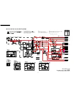
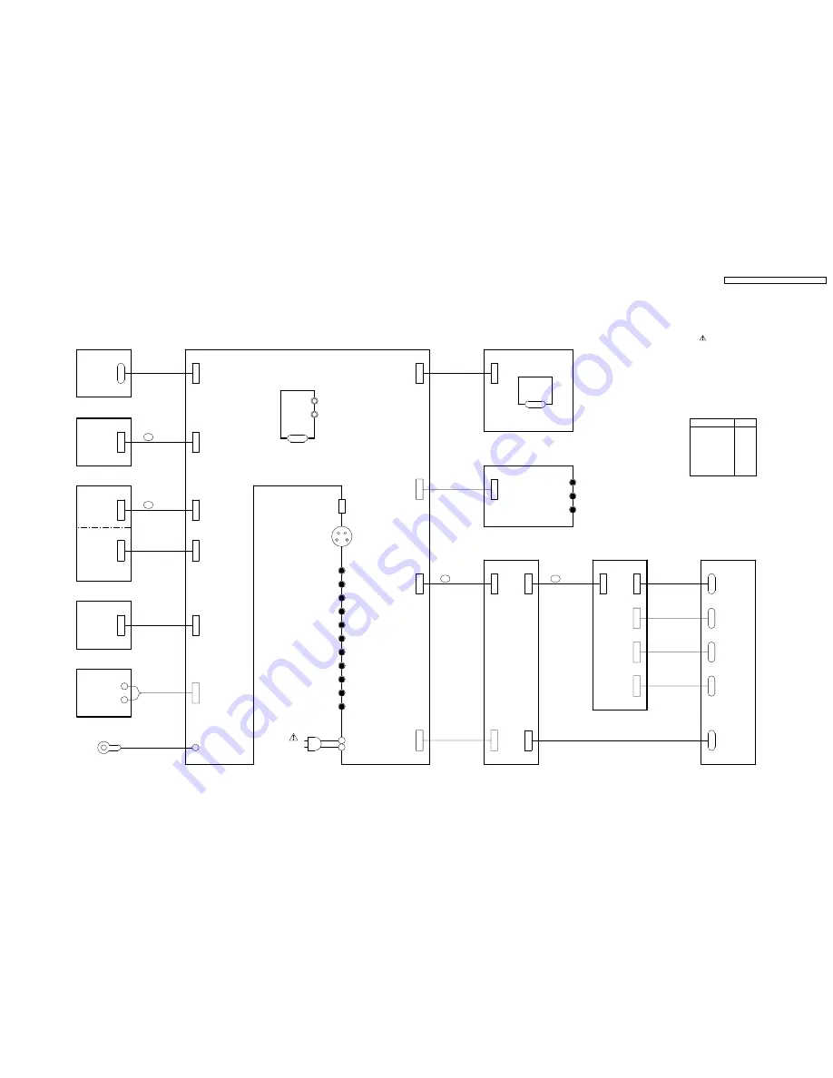
7.5. INTERCONNECTION SCHEMATIC DIAGRAM

P3002

P4591

FRONT JACK C.B.A.

(7 Pins)

P6031

P6302

OPERATION LED C.B.A.

(10 Pins)

CYLINDER UNIT

CN

P6203

(7 Pins)

752

FPC

P5002

VIDEO/Hi-Fi
AUDIO HEAD

1
2

AC CORD

P4001

AC120V

MAIN C.B.A.

PIN

FULL ERASE HEAD

P4092

P4002

AUDIO CONTROL/ERASE
HEAD UNIT

(6 Pins)

751

(2 Pins)

UHF/VHF
IN

UHF/VHF
OUT

PIN

(17 Pins)

TUNER
UHF/VHF

(3 Pins)

PIN

INFRARED
RECEIVER
UNIT

VIDEO
OUT

VIDEO
IN 1

AUDIO
OUT1 L-CH

AUDIO
IN 1 L-CH

AUDIO
OUT1 R-CH

AUDIO
IN 1 R-CH

Y
(GREEN)

PB/CB
(BLUE)

PR/CR
(RED)

P3501

GND

(1 Pin)

TO MECHANISM

   CHASSIS

(9 Pins)

OPTICAL DIGITAL
AUDIO OUT

S-VIDEO
OUT

AUDIO
OUT2 L-CH

AUDIO
OUT2 R-CH

DVD MAIN C.B.A.

P8401

P5001

(24 Pins)

309

P8801

(11 Pins)

319

DVD SUB C.B.A.

P8951

P8952

(3 Pins)

PIN

P8901

(25 Pins)

PIN

DVD MECHANISM UNIT

(11 Pins)

P8402

P1002

P6201

CAPSTAN MOTOR ASS'Y

LOADING MOTOR UNIT

(8 Pins)

(2 Pins)

P6202

P0201

+

-

P8953

(2 Pins)

PIN

P8954

(2 Pins)

PIN

P8955

(2 Pins)

PIN

VIDEO
IN 2

AUDIO
IN 2 L-CH

AUDIO
IN 2 R-CH

INTERCONNECTION SCHEMATIC DIAGRAM

INTERCONNECTION SCHEMATIC DIAGRAM

PV-D4735S/PV-D4745/PV-D4745S/PV-D4745S-K

IMPORTANT SAFETY NOTICE:
COMPONENTS IDENTIFIED BY THE SIGN      HAVE
SPECIAL CHARACTERISTICS IMPORTANT FOR SAFETY.
WHEN REPLACING ANY OF THESE COMPONENTS,
USE ONLY THE SPECIFIED PARTS.

NOTE:
FOR SCHEMATIC DIAGRAM AND CIRCUIT BOARD LAYOUT NOTES,
REFER TO BEGINNING OF SCHEMATIC SECTION.

COMPARISON CHART OF
MODELS & MARKS

PV-D4735S
PV-D4745
PV-D4745S
---------------
---------------
PV-D4745S-K

A
B
C
D
E
F

---------------

G

MODEL

MARK

PV-D4735S / PV-D4745 / PV-D4745S / PV-D4745S-K

41

Summary of Contents for OmniVision PV-D4745

Page 1: ...uthorized copying and distribution is a violation of law PV D4735S PV D4745 PV D4745S PV D4745S K DVD VCR DECK For servicing the R4 Mechanism Chassis for PV Model Please refer to the R4 Mechanism Chassis for PV Model Service Manual Order No MKE0401000C1 ORDER NO MKE0502800C1 B3 ...

Page 2: ...2 PV D4735S PV D4745 PV D4745S PV D4745S K ...

Page 3: ...ATION MARK 17 5 DISASSEMBLY ASSEMBLY PROCEDURES 18 5 1 CABINET SECTION 18 5 2 MECHANISM SECTION 21 5 3 DVD SECTION 22 6 ADJUSTMENT PROCEDURES 25 6 1 MECHANICAL ADJUSTMENT 25 6 2 ELECTRICAL ADJUSTMENT 25 6 3 TEST POINTS AND CONTROL LOCATION 26 7 SCHEMATIC DIAGRAMS 27 7 1 SCHEMATIC DIAGRAM CIRCUIT BOARD LAYOUT NOTES 27 7 2 MAIN SCHEMATIC DIAGRAMS 28 7 3 OPERATION LED FRONT JACK SCHEMATIC DIAGRAMS 35...

Page 4: ...K 1 Unplug the AC cord and connect a jumper between the two prongs on the plug 2 Measure the resistance value with an ohmmeter between the jumpered AC plug and each exposed metallic cabinet part on the equipment such as screwheads connectors control shafts etc When the exposed metallic part has a return path to the chassis the reading should be between 1 MW and 5 2 MW When the exposed metal does n...

Page 5: ... power switch is On do not place your eyes close to the front panel opening door or the other openings to look into the interior unit LASER Specification Class I level A LASER Product Class 1 level A LASER Product Wave Length 640 670 nm at DVD 770 810 nm at CD Laser Power No hazardous radiation is emitted with the safety protection 1 2 PRECAUTION OF LASER DIODE CAUTION This unit utilizes a class I...

Page 6: ...static ESD protected can generate electrical charge sufficient to damage ES devices 5 Do not use freon propelled chemicals These can generate electrical charges sufficient to damage ES devices 6 Do not remove a replacement ES device from its protective package until immediately before you are ready to install it Most replacement ES devices are packaged with leads electrically shorted together by c...

Page 7: ...In case of using high temperature soldering iron please be carefull not to heat too long Pb free solder will tend to splash when heated too high about 1100 F 600 C All products with the printed circuit board with printing must be serviced with lead free solder When soldering or unsoldering completely remove all of the solder from the pins or solder area and be sure to heat the soldering points wit...

Page 8: ...LEDs 4 1 1 Transmission check for IIC BUS The condition of IIC bus transmission before shut off is displayed 1 Press CH DOWN button on unit and 4 key on remote together in shut off or power off condition Fig 1 1 1 2 To release from this mode press any operation key on remote or turn on the power 4 SERVICE NOTES PLEASE READ Fig 1 1 2 8 PV D4735S PV D4745 PV D4745S PV D4745S K ...

Page 9: ...from this mode press any operation key on remote or turn on the power 4 1 3 Mechanism of Error Code The detecting condition and movement of mechanism is displayed 1 Press CH DOWN button on unit and 2 key on remote together in shut off or power off condition Fig 1 3 1 2 To release from this mode press any operation key on remote or turn on the power Fig 1 2 2 9 PV D4735S PV D4745 PV D4745S PV D4745...

Page 10: ...Fig 1 3 2 10 PV D4735S PV D4745 PV D4745S PV D4745S K ...

Page 11: ...t a TV Monitor 2 Set the unit to DVD mode 3 Press STOP EJECT button on the unit and 9 key on the remote controller together with no cassette inserted The unit will enter the DVD Service Mode 1 Fig 2 1 4 Press the LEFT or RIGHT key on the remote again to enter DVD Service Mode 2 Fig 2 2 Note a After replacing the DVD Unit press the CLEAR key on the remote in this mode The total elapsed Disc Motor o...

Page 12: ...onitor Fig 3 1 Note 1 After replacing the Cylinder Unit press COUNTER RESET button on remote controller in this mode Total elapsed Cylinder rotation time in hours will be cleared to 0 2 After replacing the DVD Mechanism Unit press ADD DLT button on remote controller in this mode Total elapsed DVD Play time in hours will be cleared to 0 3 To release from Usage Screen Mode press any operation button...

Page 13: ...re not to let your clothestouch the optical pickup Fig 5 1 4 6 METHOD FOR EJECTING THE DVD TRAY MANUALLY 1 Insert a Screwdriver or similar object into the Eject hole 2 Press it gently and then pull the Tray fully out Fig 6 1 4 7 SERVICE POSITION CAUTION HOT CIRCUIT Primary circuit exists on the Main C B A Use extreme care to prevent accidental shock when servicing NOTE When carring out loading of ...

Page 14: ...n the C B A and in the Service Manual Use extreme care to prevent accidental shock when servicing 4 9 SERVICE MODE In order to inhibit detection of the Supply Takeup Photo Transistors Reel Sensor and Cylinder Lock can be inhibited In this mode Mechanism movement can be confirmed When removing Cassette Up Ass y it can be confirmed without a cassette To enter Service Mode Press and hold FF and CH DO...

Page 15: ...ssette tape Set the unit into Service Mode Press CH UP button and CH DOWN button on unit together in Play back mode TRACKING CENTER will be displayed on the TV monitor In this mode the tracking is fixed at center Auto tracking and manual tracking functions are not operational Fig 11 1 To release from this mode press CH UP button and CH DOWN button on unit together again 4 12 HOW TO RESET ALL MEMOR...

Page 16: ...it and Main C B A Be careful with the direction of F F C to Connectors as shown Note 1 Insert the F F C so that it is parallel to the connector 2 After inserting the F F C check that the F F C does not incline Fig 13 2 4 14 HOW TO CONFIRM AUTO CLOCK SET FEATURE 1 Connect an RF cable from the output of one unit to the input of the test unit 2 Select corresponding RF channels 3 Playback a recording ...

Page 17: ...e above type of Power Supply Circuit a variable isolation transformer is required in order to increase the input voltage slowly 4 16 SPECIAL NOTE All integrated circuits and many other semiconductor devices are electrostatically sensitive and therefore require the special handling techniques described under the ELECTROSTATICALLY SENSITIVE ES DEVICES section of this service manual 4 17 MODEL NO IDE...

Page 18: ...assembly Flowchart Shown below When reassembling use the reverse procedure CAUTION Disconnect AC plug before disassembly or assembly 5 DISASSEMBLY ASSEMBLY PROCEDURES 5 1 CABINET SECTION 5 1 1 Disassembly Flowchart Fig C1 18 PV D4735S PV D4745 PV D4745S PV D4745S K ...

Page 19: ...Fig C2 19 PV D4735S PV D4745 PV D4745S PV D4745S K ...

Page 20: ...d tighten 7 Screws 501 502 2 Installation of Front Panel Ass y CAUTION Opener Lever may be damaged when Front Panel Ass y is installed with Cassette Door Lid of Front Panel Ass y and Opener Lever of Cassette Up Ass y set incorrectly a When installing the Front Panel Ass y swing the Cassette Door Lid all the way open until the Cassette Door tab clears the Opener Lever b Make sure that all locking t...

Page 21: ...is in the EJECT Position Fig C7 b Make sure the phase hole of the Main Cam Gear on the bottom side of Mechanism Unit is in EJECT position Fig C8 c Install the Mechanism Chassis straight onto the Main C B A so that the Photo transistor Unit 712 clears the hole in the Mechanism Chassis and that 3 Connectors P5001 P4001 P6201 are aligned and seated securely 5 2 MECHANISM SECTION Refer to the Service ...

Page 22: ...y Flowchart Perform disassembly procedures in the order described in the Disassembly Flowchart Shown below When reassembling use the reverse procedure 5 3 DVD SECTION Fig D1 22 PV D4735S PV D4745 PV D4745S PV D4745S K ...

Page 23: ...Fig D2 23 PV D4735S PV D4745 PV D4745S PV D4745S K ...

Page 24: ...ll the DVD Sub C B A with the Locking Tab and 2 bosses b Install the DVD Main C B A with the Locking Tab and the rib c Pass the leads through the slots A and B d Solder portions a b c d e f g h i j on the C B A Note Solder portions h and i while pushing down the DVD Sub C B A securely e Connect the F F C s to Connectors P8901 on the DVD Main C B A f Tighten the 2 Screws 520 5 3 1 1 Notes in chart ...

Page 25: ...rmine the Video Head Switching Point during Playback Symptom of Misadjustment May cause Head Switching Noise and or Vertical Jitter Test Point TP3001 Main C B A TP6205 Main C B A Specification T 6 H 0 5 H 0 38 ms 0 03 ms Mode SP Playback Equipment Oscilloscope VHS Alignment Tape VFMS0003H6 TV monitor 1 Insert the VHS Alignment Tape Enter service mode by pressing and holding FF and CH DOWN buttons ...

Page 26: ... Then COMP will appear on the TV monitor and adjusted value will be written to Memory IC IC6004 Fig E4 6 Press STOP button on the remote to release from EVR PG SHIFTER ADJUSTMENT MODE 6 3 TEST POINTS AND CONTROL LOCATION 26 PV D4735S PV D4745 PV D4745S PV D4745S K ...

Page 27: ...6 2V Zener Voltage 2 How to identify Connectors Each connector is labeled with a Connector No and Pin No Indicating what it is connected to in other words its counter part Use the interconnection schematic diagram to find the connection between associated connectors Example The connections between C B A s are shown below 3 Parts marked PT are not used in any models included in this service model 4...

Page 28: ...035 WA17 5 TP6205 WA7 5 TP6014 WA10 TP6004 PT TP6208 68U L6003 100U L6004 WA5 L6201 4R7U L6002 IC6001 C2CBHF000400 1 2 3 4 5 6 7 8 9 10 11 12 13 14 15 16 17 18 19 20 21 22 23 24 25 31 32 33 34 35 36 37 38 39 40 41 42 43 44 45 46 47 48 49 50 51 52 53 54 55 56 57 58 59 60 61 62 63 64 65 66 67 68 69 70 71 72 73 74 75 81 82 83 84 85 86 87 88 89 90 91 92 93 94 95 96 97 98 99 100 26 27 28 29 30 76 77 78...

Page 29: ... Main clock 12MHz OSC output terminal 40 GND OSC Digital GND for OSC circuit 41 3 58MHz IN I Not used 42 3 58MHz OUT O Not used 43 SUB CLK ST L I 5V fix 44 LC OSC IN I Input terminal of the LC Oscillation For OSD dot clock 45 LC OSC OUT O Output terminal of the LC Oscillation For OSD dot clock 46 NUB GND Connected to the GND 47 4FSC LPF I OSC Filter connection terminal for Internal sync generator ...

Page 30: ... 11 12 13 14 15 16 17 18 19 20 21 22 23 24 25 31 32 33 34 35 36 37 38 39 40 41 42 43 44 45 46 47 48 49 50 51 52 53 54 55 56 57 58 59 60 61 62 63 64 65 66 67 68 69 70 71 72 73 74 75 81 82 83 84 85 86 87 88 89 90 91 92 93 94 95 96 97 98 99 100 26 27 28 29 30 76 77 78 79 80 0 033 C4100 TP3002 WA17 5 TP3001 WA7 5 P5002 9 AR 8 A COM 7 AL 6 SP L 5 SP COM 4 SP R 3 EP L 2 EP COM 1 EP R GND VCC 75 R3100 75...

Page 31: ...AGC DET N L DE EMPH SQPB EQ Y LPF TRAP NC HP NC DEH N L EMPH ET LPF PC VIDEO AGC ATT 4dB ATT 10dB ATT 6dB ATT 10dB ATT 10dB 629 TRAP 6dBAMP C K NP CONV B D PILOT ERASE BPF PILOT ADD V AMP SQUE LCH CLEAR SYNC GCL P GCL R P R SD R SD P P R P R P R R P P R P R FEC TRAP P C ACC INT R R SVHS EXT DO DO REC SQPB R SDECK R SDECK R SDECK R SDECK SQPB R SDECK P R R ATP R P R P P R R P GND SQPB SQPB P C ACC ...

Page 32: ...00 16V C4262 1 50V C4203 10 16V C4253 10 16V C4259 10 16V C4213 1 50V C4244 2R2 50V C4208 10 16V C4206 10 16V C4235 33 6 3V C4234 10 16V 10 16V C4553 C4264 3R3 50V 10 16V C4305 10 16V C4306 Q4202 UN5115 Q4201 UN5115 Q4258 UN5215 Q4253 UN5215 Q4257 UN5215 Q4259 UN5215 Q4203 UN5215 Q4254 UN5215 Q4204 UN5215 IC4302 C1AB00001731 IC4301 C1AB00001731 TP4207 WA17 5 IC4201 AN3663FBP V 1 2 3 4 5 6 7 8 9 10...

Page 33: ...H AGC GND PREAMP SWITCH VCC REC DC2 HIFI PLAY H NOISE DET PNR RCH BPF BPF LPF FM MODULATOR DEMODULATOR AGC SWITCH MUTE REC AGC ADJ GND VCC FSC MTS MUTE IIC BUS INTERFACE REC AUDIO SIGNAL PB AUDIO SIGNAL VCC MTS MTS SAP DEMODULATOR DEMODULATOR BLOCK DBX NOISE REDUCTION TUNER SWITCH SPECTRAL DET SPECTRAL TIMING VREF WIDE BAND TIMING GND L WIDE BAND DET L R REF MTS LED IC4201 Hi Fi AUDIO MTS SAP SIGN...

Page 34: ..._ 6 5V TO DVD MAIN C B A P8402 3 3V SWITCHING REGULATOR 6 5V SWITCHING REGULATOR PRIMARY SIDE GND CONSTANT VOLTAGE CONSTANT VOLTAGE CONSTANT VOLTAGE CONSTANT VOLTAGE FEED BACK SHUNT REGULATOR 5V SWITCHING REGULATOR 46 TO M I TO M I 14 TO M I 13 TO M I 33 TO M III 81 82 TO M III 83 TO M III 8 TO M I M II M III 7 TO M I 11 TO M I 10 TO M I TO M I M II M III 1 TO M I 12 TO M I 9 51 TO M II 12V SWITCH...

Page 35: ...L VIDEO IN AUDIO IN R AUDIO_R_IN2 GND GND GND AUDIO_L_IN2 VIDEO_IN2 KEY_IN_1 VCR DVD POWER TO MAIN C B A P3002 REC AUDIO SIGNAL REC VIDEO SIGNAL NOTE FOR SCHEMATIC DIAGRAM AND CIRCUIT BOARD LAYOUT NOTES REFER TO BEGINNING OF SCHEMATIC SECTION NOTE For placing a purchase order of the parts be sure to use the part number listed in the parts list Do not use the part number on this diagram NOTE PARTS ...

Page 36: ...004 1 10 C8038 10 C8023 10 C8021 10 C8030 10 C8026 10 C8028 10 C8022 C8035 1 C8048 0 1 C8033 0 033 C8049 0 1 C8054 1 C8040 5600P C8047 0 1 C8037 1 C8057 1 C8050 0 1 C8044 0 1 C8039 1 C8051 1 C8045 0 1 C8055 1 C8042 0 018 C8058 10 C8052 10 C8071 10 TP8032 PT TP8033 PT TP8034 PT R8056 1K IC8004 1 A0 2 A1 3 A2 4 VSS 5 SDA 6 SCL 7 WP 8 VCC R8065 6R8 L8011 J0JCC0000215 L8012 J0JCC0000215 L8013 J0JCC000...

Page 37: ...5 46 47 48 49 50 51 52 53 54 VDD DQ0 VDDQ DQ1 DQ2 VSSQ DQ3 DQ4 VDDQ DQ6 VSSQ DQ7 VDD LDQM WE CAS RAS SDRAM data 5 CS I O I SDRAM chip select low DQ5 3 3V I SDRAM data 0 I O 3 3V I SDRAM data 1 I O SDRAM data 2 I O Ground SDRAM data 3 I O SDRAM data 4 I O 3 3V I I O SDRAM data 6 Ground I O SDRAM data 7 I 3 3V I Data input output mask I Write enable low I Column address strobe low I Row address stro...

Page 38: ...20 6 3V C8430 330 6 3V C8403 22 6 3V C8441 C8455 22 6 3V 100 6 3V C8452 100 6 3V C8448 100 6 3V C8453 22 6 3V C8449 22 6 3V C8445 100 6 3V C8444 C8454 22 6 3V 100 6 3V C8450 22 6 3V C8451 FL8501 PT FL8502 J0HAAG000015 PT FL8402 PT Q8501 PT Q8502 PT Q8503 Q8504 UN5215 Q8505 UN5215 IC8501 C0FBBK000035 1 BCK 2 DATA 3 LRCK 4 DGND 5 VDD 6 VCC 7 VOUTL 8 VOUTR 11 ZEROR ZEROA 12 ZEROL NA 13 MD 14 MC 15 ML...

Page 39: ... 1 MUTE3 2 BIAS1 3 MUTE1 4 MUTE2 5 SPIN 6 TRVIN 7 LDIN 8 VCC3 9 LDM 10 LDM 21 VCC45 22 FOIN 15 TK 16 TK 17 FO 18 FO 19 PGND 20 VCC12 11 TRVM 12 TRVM 23 TKIN 24 GND 13 SPM 14 SPM 25 OPIN 26 OPIN 27 OPOUT 28 BIAS2 TO DVD MECHANISM UNIT TO DVD SUB C B A P8951 SERVO DRIVER SWITCHING SWITCHING DRIVE DRIVE AMP AMP 30 TO DVD M I TO DVD M I 28 27 TO DVD M I TO DVD M I 14 TO DVD M II 44 5 TO DVD M I TO DVD...

Page 40: ...ISM UNIT TO DVD MAIN C B A P8801 TO DVD MECHANISM UNIT TO DVD MECHANISM UNIT TO DVD MECHANISM UNIT ESE31L01T NOTE FOR SCHEMATIC DIAGRAM AND CIRCUIT BOARD LAYOUT NOTES REFER TO BEGINNING OF SCHEMATIC SECTION NOTE For placing a purchase order of the parts be sure to use the part number listed in the parts list Do not use the part number on this diagram NOTE PARTS MARKED PT ARE NOT USED DVD SUB SCHEM...

Page 41: ...8401 P5001 24 Pins 309 P8801 11 Pins 319 DVD SUB C B A P8951 P8952 3 Pins PIN P8901 25 Pins PIN DVD MECHANISM UNIT 11 Pins P8402 P1002 P6201 CAPSTAN MOTOR ASS Y LOADING MOTOR UNIT 8 Pins 2 Pins P6202 P0201 P8953 2 Pins PIN P8954 2 Pins PIN P8955 2 Pins PIN VIDEO IN 2 AUDIO IN 2 L CH AUDIO IN 2 R CH INTERCONNECTION SCHEMATIC DIAGRAM INTERCONNECTION SCHEMATIC DIAGRAM PV D4735S PV D4745 PV D4745S PV ...

Page 42: ... 96 2 6 2 6 97 2 6 2 6 98 5 2 5 2 99 5 2 5 2 100 0 0 IC6002 1 1 2 1 2 2 0 0 3 0 0 4 4 7 4 7 IC6003 1 2 4 2 4 2 1 2 1 2 3 0 0 4 5 1 5 1 IC6004 1 0 0 2 0 0 3 0 0 4 0 0 5 3 0 3 0 6 3 3 3 3 7 0 0 8 5 0 5 0 IC6005 1 5 2 5 2 2 5 2 5 2 3 0 0 4 0 0 5 5 2 5 2 6 0 0 IC6201 1 11 9 11 8 2 1 8 1 8 3 0 0 4 0 3 0 3 5 0 0 6 0 0 7 16 5 16 5 8 0 0 9 2 8 2 8 10 1 6 1 6 11 1 6 1 6 12 0 7 0 7 13 1 5 1 5 14 2 5 2 5 15 ...

Page 43: ...14 0 15 0 16 2 6 17 0 8 18 2 6 19 2 5 20 2 1 21 2 1 22 2 1 23 0 24 2 1 25 5 26 2 1 27 0 28 4 1 29 1 5 30 0 8 31 0 1 32 2 5 33 2 5 34 0 7 35 2 5 36 0 37 1 7 38 0 39 40 5 41 0 42 3 6 43 3 4 44 2 3 45 0 46 3 3 47 2 2 48 2 2 49 3 4 50 3 3 51 5 52 3 3 53 6 54 2 5 55 0 56 0 57 6 58 12 2 59 5 9 60 0 2 61 2 5 62 2 5 63 2 7 64 0 6 Q1001 S 0 G 1 9 D 155 Q1002 S 155 G 161 D 111 Q1003 E 0 C 1 9 B 0 Q1004 1 0 ...

Page 44: ... 10 11 12 0 13 14 3 3 15 2 4 16 0 17 3 2 18 3 3 19 3 0 20 2 3 21 1 7 22 23 24 25 26 27 3 3 28 0 29 30 31 32 33 34 35 36 37 3 3 38 3 3 39 1 5 40 41 0 42 43 3 3 44 45 46 0 47 48 49 3 3 50 51 52 0 53 54 0 IC8004 1 0 2 0 3 0 4 0 5 3 3 6 3 2 7 0 8 3 3 IC8005 1 1 2 2 1 1 3 3 3 4 3 3 5 0 6 0 7 2 2 8 2 2 IC8401 1 5 0 2 0 1 3 0 1 4 2 1 5 5 0 6 1 0 7 0 8 1 5 9 2 2 10 0 11 1 5 12 0 13 2 1 14 5 0 15 2 2 16 4 ...

Page 45: ...59 R6061 R6068 J1003 R6060 R6062 R6171 R6065 R6050 C6156 R6058 R3028 R6158 R6166 R6172 R6114 D6001 R6109 R6115 C6072 C6405 C6406 R6069 C6071 R6071 C6080 R6080 C6078 R6075 R6087 R6100 1 30 31 50 51 80 81 100 1 13 26 14 R6220 R6222 R6223 R6225 C6223 C6225 R6219 R6224 C6201 C6208 C6213 C6212 C6209 C6210 C6098 C6092 C6096 C6211 C6206 C1305 C6219 C6215 C6222 C6203 L4804 J8005 L4801 P5001 P6203 P6202 C4...

Page 46: ...S MODELS FOR PROPER PARTS CONTENT FOR THE MODEL YOU ARE SERVICING PLEASE REFER TO THE SCHEMATIC DIAGRAM AND PARTS LIST NOTE CIRCUIT BOARD LAYOUT INCLUDES COMPONENTS WHICH ARE NOT USED NOTE FOR SCHEMATIC DIAGRAM AND CIRCUIT BOARD LAYOUT NOTES REFER TO BEGINNING OF SCHEMATIC SECTION NOTE CIRCUIT BOARD LAYOUT SHOWS COMPONENTS INSTALLED FOR VARIOUS MODELS FOR PROPER PARTS CONTENT FOR THE MODEL YOU ARE...

Page 47: ...9 C8553 C8552 L8420 L8418 L8419 L8422 L8421 L8434 L8431 L8424 L8504 L8433 L8435 L8436 L8437 R8802 R8801 C8803 C8813 C8807 C8806 C8805 C8804 C8810 C8811 Q8503 Q8502 C C E E B B C8555 C8554 R8558 R8550 C8536 R8501 R8517 R8502 L8413 R8520 R8535 R8536 C8545 L8409 C8443 C8431 R8569 TP8523 R8572 C8504 C8506 L8408 C8424 R8410 C8420 C8423 C8413 C8418 L8405 R8401 R8403 R8409 C8415 R8425 R8420 Q8401 R8407 C...

Page 48: ...PV D4735S PV D4745 PV D4745S PV D4745S K 48 ...

Page 49: ...WITCHING 12V 2 3 1 POWER ON H FROM IC6001 83 D1025 D1041 D1002 T1001 MAIN C B A C1007 D1004 L1001 3A 125V 250V F1001 KILLER SURGE RECTIFIER FILTER LINE 8 7 5 4 2 DIAGRAM BLOCK TO DVD I 10 SW 5V DVD P1002 9 SW 3 3V DVD P1002 8 SW 3 3V DVD P1002 4 P1002 M VM 6V M VM 6V 3 P1002 Q1013 30V POWER ON SWITCHING 2 3 4 10 11 14 1 3 BACK FEED REGULATOR SHUNT VOLTAGE CONSTANT D1032 L1010 Q1003 Q1005 Q1001 Q10...

Page 50: ...M IC6001 81 SP L Q4150 FROM IC6001 23 HIFI ADJUSTMENT H FROM IC6001 71 IIC CLOCK FROM IC6001 18 VIDEO HEAD SW FROM IC6001 13 V LOCK PULSE FROM IC6001 72 IIC DATA TO IC6001 9 TRACKING ENVELOPE TO IC6001 85 S VHS PB H TO IC6001 48 FSC TO IC4201 45 1 4 OSC BUFFER BUFFER BUFFER BUFFER Q3030 P5002 5 P5002 4 P5002 6 VIDEO SP L HEAD VIDEO SP R HEAD P5002 2 P5002 1 P5002 3 VIDEO SLP L HEAD VIDEO SLP R HEA...

Page 51: ...ER UNIT IC4201 Hi Fi AUDIO SIGNAL PROCESS AGC DET L R Hi Fi AUDIO L HEAD Hi Fi AUDIO R HEAD AGC AMP REC AMP AUDIO OUT2 R CH AUDIO OUT2 L CH AUDIO OUT1 R CH AUDIO OUT1 L CH R R R L L L MUTE MUTE REC AUDIO SIGNAL PB AUDIO SIGNAL AUDIO IN 2 R CH AUDIO IN 2 L CH MATRIX MUTE CONTROL FROM Q4150 C 1 4 OSC 8 P5002 9 P5002 7 P5002 P5001 15 P5001 13 DVD AUDIO R CH DVD AUDIO L CH TP4002 TP4207 FROM DVD II BL...

Page 52: ...APSTAN MOTOR ASS Y CYLINDER UNIT AUDIO CONTROL ERASE HEAD EJECT DOWN R REW LOAD REV PLAY POWER OFF STOP R STOP F FF REW FF2 PIN NO OF IC6001 MODE SW1 33 SW2 32 SW3 31 SW4 30 L L H L H L H L H L L H H H H L L H H L L L H H H L L H H H H L L H H H H L L L L L L H H H H H SW6001 MODE SELECT SWITCH TP6206 RESET RESET Q6003 Q6004 Q6005 Q6008 TP6013 TP6020 5V IR RECEIVER U6302 IIC DATA 5 34 78 D6315 DVD...

Page 53: ...OR CONTROL 22 TRACKING MOTOR CONTROL 23 75 TRAVERSE MOTOR CONTROL 6 76 SPINDLE MOTOR CONTROL 5 148 147 CLOSE OPEN SW8952 SW8951 6 5 8 59 IC8004 EEPROM 60 I2 C SERIAL CLOCK I2 C SERIAL DATA VCC I2 C SERIAL CLOCK I2 C SERIAL DATA IC8001 DVD SIGNAL PROCESSOR DVD MICROCONTROLLER P8901 3 P8901 21 V REF HFM 127 77 V REF H HFMON P8402 4 P8402 10 P8402 8 9 M VM 6V P8402 3 ACT VM 6V SW 5V SW 3 3V 8 20 21 D...

Page 54: ...FILTER MODULATOR 27MHz OSC VIDEO ENCODER DVD CD FORMATTER DVD DECODER ERROR CORRECTION ECC VIDEO I F RF SIGNAL PROCESS AUDIO I F TO AUDIO BLOCK DIAGRAM A MUTE P8401 6 TO VIDEO BLOCK DIAGRAM 57 54 56 22 26 29 35 192 195 197 200 203 204 206 208 210 212 21 23 25 27 30 33 36 37 39 43 45 47 50 51 217 220 221 223 224 226 228 230 233 237 238 2 4 5 7 8 10 11 13 42 44 45 47 48 50 51 53 1 2 4 5 7 8 10 11 13...

Page 55: ...in 30sec IC6001 will switch automatically to VCR Check the VCR mode indicator and DVD mode indicator on the Front Light up Indicators Check the voltage during the 30 seconds during which the unit remains in DVD mode First confirm that the Main C B A is O K other than DVD Mechanism Unit and DVD Main C B A by referring to Communication Timing Chart 1 and Communication Timing Chart 2 Check points 1 A...

Page 56: ...0 mV 400 mVp p Check the voltage at TP8906 on the DVD Main C B A Is it 5 0 V Replace the Q8905 and Q8906 on the DVD Main C B A Replace the IC8001 on the DVD Main C B A NG OK NG OK Note Check the voltage during 10 to 20 seconds as soon as disc has been inserted OK Repair the around circuit of SW_ 5V_DVD line NG Check the voltage at TP8903 on the DVD Main C B A Is it 5 0 V Check the voltage at Q8905...

Page 57: ...Component Side Foil Side TP8958 TP8523 Q8906 C B E IC8001 TP8011 TP8006 TP8010 TP8005 TP8809 TP8807 TP8009 TP8806 TP8813 TP8812 TP8916 TP8923 Q8905 C B E TP8906 TP8903 IC8801 TP8823 PV D4735S PV D4745 PV D4745S PV D4745S K TROUBLESHOOTING HINTS TEST POINTS LOCATION PV D4735S PV D4745 PV D4745S PV D4745S K 57 ...

Page 58: ...PV D4735S PV D4745 PV D4745S PV D4745S K 58 ...

Page 59: ...10 EXPLODED VIEWS 10 1 MECHANISM SECTION 59 PV D4735S PV D4745 PV D4745S PV D4745S K ...

Page 60: ...10 2 DVD SECTION 60 PV D4735S PV D4745 PV D4745S PV D4745S K ...

Page 61: ...10 3 CHASSIS FRAME AND CASING PARTS SECTION 61 PV D4735S PV D4745 PV D4745S PV D4745S K ...

Page 62: ...10 4 PACKING PARTS AND ACCESSORIES SECTION 62 PV D4735S PV D4745 PV D4745S PV D4745S K ...

Page 63: ...al Chassis Sub Ass y Ref No 4 consists of all the mechanical parts except the Cylinder Kit Ref No 1 and the Cassette Up Ass y Ref No 51 After replacing the Mechanical Chassis Sub Ass y be sure to perform TAPE INTERCHANGEABILITY ADJUSTMENT in Service Manual for R4 Mechanism Chassis for PV Model Order No MKE0401000C1 3 Cylinder is supplied as a Cylinder Kit Ref No 1 only Cylinder Kit consists of a C...

Page 64: ...1 VYPS7181 FRONT PANEL ASS Y B 3 71 VYPS7178 FRONT PANEL ASS Y C F 3 72 LSGP0457 CASSETTE DOOR LID A C F 3 72 LSGP0458 CASSETTE DOOR LID B 3 73 LSKM1124 TOP PANEL A C F 3 73 LSKM1125 TOP PANEL B 3 74 LSMK0858 BOTTOM COVER 3 75 LSMK0859 REAR COVER 3 76 VKA0364 FOOT 2 3 77 LSMB0310 CASSETTE DOOR SPRING 3 78 LSGP0459 DVD DOOR LID A 3 78 LSGP0464 DVD DOOR LID B 3 78 LSGP0461 DVD DOOR LID C F 3 79 LSMB...

Page 65: ...101RLL1 IC LINEAR IC1003 B1AZKD000001 IC LINEAR or IC1003 C0DAEMB00004 IC LINEAR or IC1003 C0DAEMZ00005 IC LINEAR IC1004 C0CBCDD00012 IC LINEAR IC1005 C0DBZHG00012 IC LINEAR IC1006 C0DBZGG00010 IC LINEAR IC1301 C0DBZJG00007 IC LINEAR IC1302 C0CBCDC00052 IC LINEAR IC3001 C1AB00002002 IC LINEAR IC3301 C1AB00001731 IC CMOS STANDARD LOGIC E S D IC4201 AN3663FBP V IC LINEAR IC6001 C2CBHF000400 IC 16BIT...

Page 66: ...B1ADCC000004 TRANSISTOR SI PNP CHIP or Q6009 B1ADCF000001 TRANSISTOR SI PNP CHIP or Q6009 B1ADCF000077 TRANSISTOR SI PNP CHIP DIODES Ref No Part No Part Name Description Remarks D1002 ERZV07Z361CS SURGE ABSORBER Ref No Part No Part Name Description Remarks D1004 B0EDKT000009 DIODE SI D1012 B0JANK000003 DIODE SI D1013 B0JAME000079 DIODE SI or D1013 B0JAME000049 DIODE SI or D1013 B0JANE000028 DIODE ...

Page 67: ...P 1 16W 47K R4219 ERJ3GEYJ822V MGF CHIP 1 16W 8 2K Ref No Part No Part Name Description Remarks R4220 ERJ3GEYJ822V MGF CHIP 1 16W 8 2K R4224 ERJ3GEYJ822V MGF CHIP 1 16W 8 2K R4225 ERJ3GEYJ822V MGF CHIP 1 16W 8 2K R4230 ERJ3GEYJ152V MGF CHIP 1 16W 1 5K R4231 ERJ3GEYJ152V MGF CHIP 1 16W 1 5K R4236 ERJ3GEY0R00V MGF CHIP 1 16W 0 R4237 ERJ3GEYJ393V MGF CHIP 1 16W 39K R4253 ERJ3GEYJ102V MGF CHIP 1 16W 1...

Page 68: ...5 F2A1E3310040 ELECTROLYTIC 25V 330UF C1036 ECJ1VB1C105K C CHIP 16V 1UF Ref No Part No Part Name Description Remarks C1037 F2A1E3310040 ELECTROLYTIC 25V 330UF C1038 F1J1C1050011 C CHIP 16V 1UF C1039 F1J1C1050011 C CHIP 16V 1UF C1040 ECA1VHG101I ELECTROLYTIC 35V 100UF C1041 ECA1HHG470I ELECTROLYTIC 50V 47UF C1043 ECJ1VB1C105K C CHIP 16V 1UF C1045 EEUFF1A221H ELECTROLYTIC 10V 220UF C1046 ECEA1HKAR47...

Page 69: ...5085 ECJ1VB1E103K C CHIP 25V 0 01UF C5087 ECJ1VB1E103K C CHIP 25V 0 01UF C5089 ECJ1VB1E103K C CHIP 25V 0 01UF C5091 ECJ1VB1E103K C CHIP 25V 0 01UF C6034 ECJ1VF1E104Z C CHIP 25V 0 1UF Ref No Part No Part Name Description Remarks C6037 ECEA0JKA101 ELECTROLYTIC 6 3V 100UF C6038 ECJ1VC1H180J C CHIP 50V 18PF C6039 ECJ1VC1H220J C CHIP 50V 22PF C6044 ECJ1VC1H101J C CHIP 50V 100PF C6045 ECJ1VC1H820J C CHI...

Page 70: ...A TRANSFORMER Ref No Part No Part Name Description Remarks T1001 LSTP0128 SW TRANSFORMER T4101 G2A472C00003 TRANSFORMER JACKS Ref No Part No Part Name Description Remarks JK3001 K2HA612B0035 AUDIO VIDEO JACK SOCKET JK3003 K2HZ105B0007 S VHS JACK SOCKET JK3004 K2HA507B0003 AUDIO VIDEO JACK SOCEKT JK4801 B3RAE0000030 IC LINEAR PRINTED CIRCUIT BOARD ASSEMBLY Ref No Part No Part Name Description Remar...

Page 71: ... SI NPN CHIP or Q8905 B1GBCFJJ0035 TRANSISTOR SI NPN CHIP Q8906 UNR511500L TRANSISTOR SI PNP CHIP or Q8906 B1GDCFJA0017 TRANSISTOR SI PNP CHIP or Q8906 B1GDCFJJ0025 TRANSISTOR SI PNP CHIP DIODES Ref No Part No Part Name Description Remarks D8001 MA2J111008 DIODE SI or D8001 B0ACCK000005 DIODE SI or D8001 MA2J11100L DIODE SI RESISTORS Ref No Part No Part Name Description Remarks R8001 ERJ3GEYJ102V ...

Page 72: ... 1UF C8012 ECJ1VB0J105K C CHIP 6 3V 1UF C8013 ECJ1VB0J105K C CHIP 6 3V 1UF Ref No Part No Part Name Description Remarks C8014 ECJ1VB0J105K C CHIP 6 3V 1UF C8015 ECJ1VB0J105K C CHIP 6 3V 1UF C8016 ECJ1VB0J105K C CHIP 6 3V 1UF C8017 ECJ1VB0J105K C CHIP 6 3V 1UF C8018 ECEA0JKA331 ELECTROLYTIC 6 3V 330UF C8019 F1H1C104A041 C CHIP 16V 0 1UF C8020 ECJ1VB0J105K C CHIP 6 3V 1UF C8021 ECJ2FB0J106K C CHIP 6...

Page 73: ...C1H560J C CHIP 50V 56PF C8922 ECJ1VC1H560J C CHIP 50V 56PF FILTERS Ref No Part No Part Name Description Remarks FL8502 J0HAAG000015 EMI FILTER CHIP COILS Ref No Part No Part Name Description Remarks L8001 J0JCC0000117 EMI FILTER CHIP L8002 J0JDC0000002 EMI FILTER CHIP L8005 J0JDC0000002 EMI FILTER CHIP L8006 J0JCC0000215 EMI FILTER CHIP L8007 J0JDC0000002 EMI FILTER CHIP L8008 J0JDC0000002 EMI FIL...

Reviews: