background image


Operation manual for Narrow-pitch connectors P4S Shield type


Panasonic Corporation
industrial.panasonic.com/ac/e/ 


©

 Panasonic Corporation 2017 

ACCTF24E-1   201710 


14


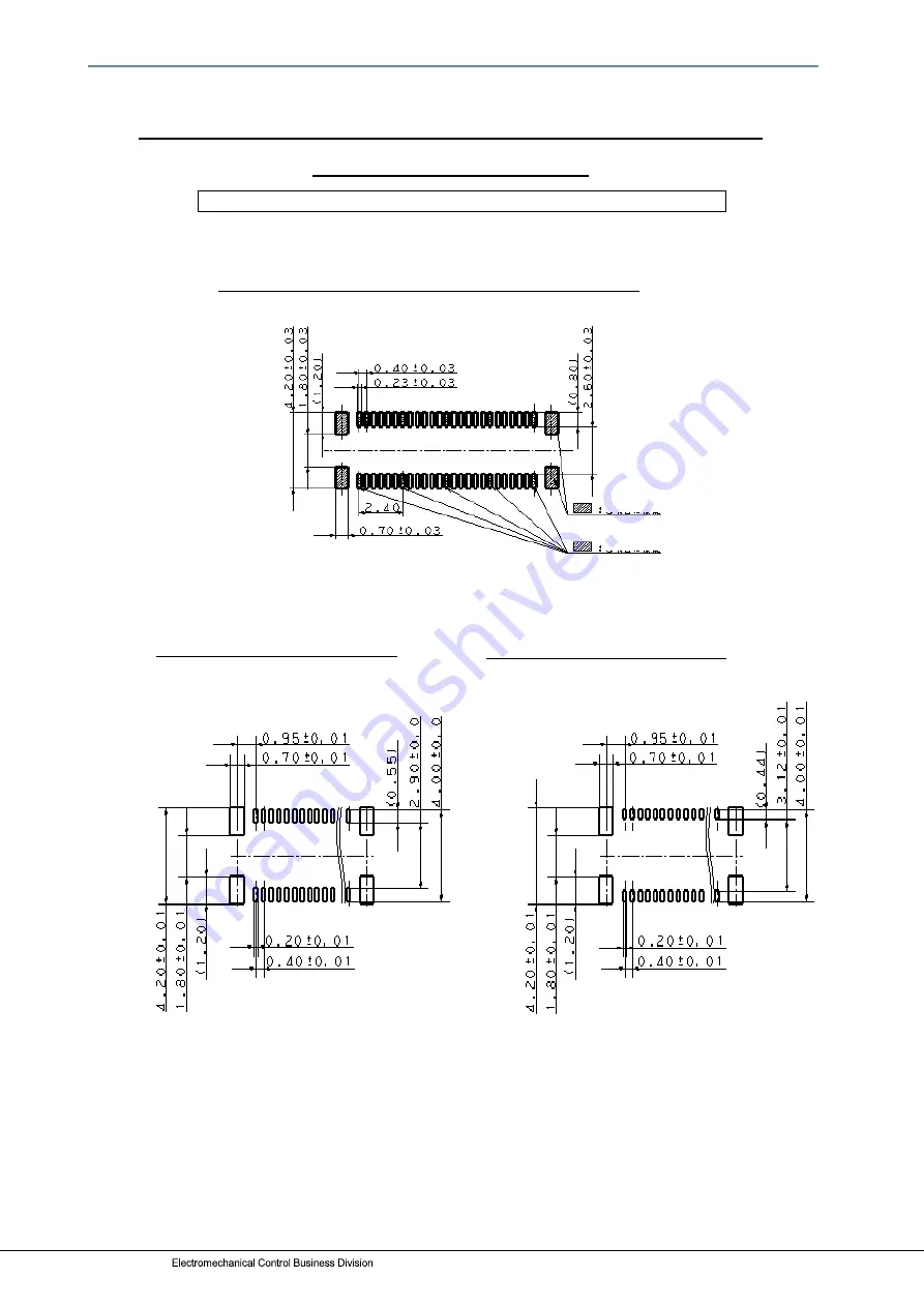
Recommended specifications of mounting pattern on PC board and  

window size of metal masking 

Please refer to the latest product specifications when designing your product.       


Product: Narrow pitch connector P4S Shield type Socket 


Recommended mounting pattern on PC board (Top view)


Thickness of metalmasking:120

μ

(Terminal part window ratio:60%) 
(Metal bracket part window ratio:100%) 

Thickness of metalmasking:150

μ

(Terminal part window ratio:48%) 
(Metal bracket part window ratio:100%) 

Connect to GND 

Connect to GND 

(2.40 mm pitch) 

Summary of Contents for P4S

Page 1: ...ACCTF24E 1 2017 10 industrial panasonic com ac e P4S Shield type Narrow pitch Connectors Operation manual ...

Page 2: ...ndustrial panasonic com ac e Panasonic Corporation 2017 ACCTF24E 1 201710 1 Contents 01 Introduction 2 02 Precautions for equipment design 3 03 Precautions for mounting and reflow soldering 15 04 Precautions for mating 23 Parts that require special confirmation are bold and underlined ...

Page 3: ...starting production Difference between P4S and P4S Shield type P4S P4S Shield type Space saving Width 3 6 mm Width 3 8 mm Contact reliability Drop resistance Bellows contact Adopted Bellows contact Adopted Mountability Requires dedicated nozzle Requires dedicated nozzle Noise immunity Multi point ground Shield construction Pin layout Unlimited Ground dedicated terminal available 3 6mm 3 8mm Pickup...

Page 4: ...isaligned connector positions may cause mating failure or product breakage Panasonic corporation does not guarantee the failures caused by using the multiple connectors 2 Solid board is tend to warp to vertical direction against mill direction of production process Some warp directions can cause poor soldering Therefore arrange the board in a direction that can minimize warp This gap causes poor s...

Page 5: ...connector be placed in a position that does not require swing motion of the mounter during pickup and mounting The inertial force of the swing motion of mounter often displaces the connectors so that connector arrangement without swing operation is required Connector arrangement with swing motion rotation during picking up and mounting Pickup positions Connector Embossed tape Main board No inertia...

Page 6: ...is not enough as the lower chart the connector is affected by the load of the inertial force and might be damaged Please consider as follows Shock of fall 1 If the both boards are not fixed sufficiently the connector is affected by the shock and might be damaged 2 If there is no gap between enclosure and sub board A B the sub board strikes against the enclosure Due to the impact of its strike the ...

Page 7: ...201710 6 3 For an easier connecting operation it is recommended that the main board be designed as follows Provide a positioning mark Place the connector in a position where a connector mating operation can be easily checked Flexible PC board Support plate Main board Positioning mark silk screening printing pattern copper leaf Positioning mark example ...

Page 8: ...r an area where through holes are prohibited is indicated on the underside of the connector Make sure to note this area Since the terminal soldering face is configured to extend to the bottom face of the molded part a defect that cannot be reworked occurs if a solder bridge is created on this part To lead out the pattern by a through hole using the bottom face of the connector design by referring ...

Page 9: ...ucted as shown in below the post is extended to the bottom of body and metal part of the terminal is exposed horizontally on the arm from the post on the bottom of body to the middle of foot pattern If an isolated through hole is placed in prohibited area the gap between pattern and contacts may become too wide so that poor soldering may be occurred interference in contiguous contacts interference...

Page 10: ...g a through hole Prevent solder from reaching the land by using a cover lay or resist 7 Please consider the following point as a pattern peeling preventive measure when removing the connector Make the foot pattern length longer than the coverlay opening In general at least 0 3 mm 8 Foot pattern dimensions indicated in the specification intended to achieve the minimum area on the premise that the r...

Page 11: ... warpage is more likely to occur if a pattern is laid in a line or if the copper foil is applied over the entire FPC board for noise prevention purposes It is difficult to keep FPC flat because FPC is flexible Example of carrier for mounting process Magic resin Daisho Denshi Silicon gum board Mitsubishi Resin Assist carrier ShinEtsu Polymer Co Ltd When mounting connector it is recommended that the...

Page 12: ...ation layer Generally the coverlay thickness is set to about 30 μm including the adhesive If the thickness exceeds 30 μm remove the coverlay under the connector from the design 3 This connector can be used for main board to FPC connection In case that the flexible board is too short excessive load affects the connector and may be shifted out Please design as the flexible board is appropriately sla...

Page 13: ...efore please make sure the support plate is sufficiently hard 4 As a rule always cut the support plate materials into pieces in the same direction otherwise some plates will warp during reflow soldering and cause poor soldering It is recommended to cut the material in the direction of the reinforcing fiber 5 Design the support plates so that the edges are 0 5 1 0 mm or more outside the tips of the...

Page 14: ...g Please make sure to adjust the amount of solder applied after checking the finish quality in a test run 2 Compared with natural air reflow soldering N2 reflow soldering can reduce oxidization of the melted solder surface This significantly improves the solder wettability Therefore please make sure to apply an appropriate amount of solder 3 Do not apply an excessive amount of solder otherwise sol...

Page 15: ...of metal masking Please refer to the latest product specifications when designing your product Product Narrow pitch connector P4S Shield type Socket Recommended mounting pattern on PC board Top view Thickness of metalmasking 120μm Terminal part window ratio 60 Metal bracket part window ratio 100 Thickness of metalmasking 150μm Terminal part window ratio 48 Metal bracket part window ratio 100 Conne...

Page 16: ...ow size of metal masking Product Narrow pitch connector P4S Header When using shield type socket Stacking height 1 5 mm type Recommended mounting pattern on PC board Top view Thickness of metalmasking 120μm Terminal part window ratio 60 Metal bracket part window ratio 100 Thickness of metalmasking 150μm Terminal part window ratio 49 Metal bracket part window ratio 100 Connect to GND Insulation are...

Page 17: ...an the connector s weight Theoretical lifting force gr Vacuum pressure mmHG 760 10 33 Nozzle area mm2 Sample vacuum pressure of machines 480 to 520 mmHG 1 Nozzle for picking up sockets 1 The width that can be used for pickups is 0 70mm The pickup face is in the bottom between the contacts If it is difficult to secure the positioning accuracy we recommend to use the nozzle which can cover the matin...

Page 18: ... the cover in calculation theory However there is difference in socket s speed of moving or rolling Conformation is needed 2 Nozzle tip shape example for header side Circular nozzle tip Oval shaped nozzle Note It is possible to pick up the cover in calculation theory However there is difference in socket s speed of moving or rolling Conformation is needed Circular nozzle tip Oval shaped nozzle Siz...

Page 19: ...hery it is possible that the amount of solder applied was excessive or that wicking has occurred In this case check the amount of solder applied and the temperature at the connector mounting position Special care is required with an N2 reflow oven 4 Larger front fillets can be achieved by extending the screen opening outward and shifting the solder application position outward 5 Take the following...

Page 20: ...t 2 During solder rework solder should be supplied at and the soldering iron should be applied to the tip of each pattern trace on the PC board in order to minimize contact with the terminals 3 When carrying out manual soldering or solder rework avoid using flux if possible in order to prevent it from rising to the contact section For details see the next page 4 When using flux apply as little as ...

Page 21: ... amount of solder to be applied is recommended e g BON 102F made by Japan Bonkote Co Ltd 2 Selection of soldering iron for lead free solder in particular Recommendation for 0 4 mm narrow pitch connectors Cutter blade shaped iron tip BJ7 KF made by Japan Bonkote Co Ltd Iron tip with a temperature sensor Temperature controllable iron tip In addition it is necessary to check whether or not the displa...

Page 22: ...de the iron tip on the foot pattern along the terminals without touching them Apply the soldering iron to the foot pattern to heat it Complete soldering in 1 or 2 seconds Connector s resistance to soldering heat 300 C 5 sec max 350 C 3 sec max Thin wire solder with a diameter of 0 3 0 4 mm is recommended Final soldering is recommended after provisionally soldering the terminals at both ends Note t...

Page 23: ...perations prepare equipment for cleaning process beginning with boil cleaning ultrasonic cleaning and then vapor cleaning 2 Carefully oversee the cleanliness of the cleaning fluids to make sure that the contact surfaces do not become dirty from the cleaning fluid itself 3 Since some powerful cleaning solutions may dissolve molded components of the connector and wipe off or discolor printed letters...

Page 24: ...The positioning mark described in Page 5 will help this tentative positioning 2 Slightly move the connector of the flexible PC board in the X and Y directions to check that the connector position is correct 3 Lightly press the connector until mating between the simple locking sections and mating between the contacts and posts are completed A snapping sound will indicate that the simple locking sec...

Page 25: ... of the contacts and post Generation of molded resin deformation and resin particles causing contact failures due to debris and spring return failures due to resin deformation Extreme caution is required for fitting dual sided PC boards as it is difficult to confirm their fitting position Please avoid especially the slant fitting longer direction Press fitting with the socket and header out of ali...

Page 26: ...the same time the angle should be within 40 for making the next operation 2 easier 2 Setting within 20 and press the header in the image of making the slant flat In case that the mating operation is too tight please note that there is a possibility that the angle is over 20 3 Mating completion can be confirmed by the flat gap between the boards In case of mated height 1 5 2 5 mm the angle should b...

Page 27: ...f an unmating jig shown on the following page is also recommended 4 If the unmating method described above is not feasible due to the lack of space around the connector lift around the holding metal piece as shown below to unmate the connector If the number of pins is small lift around the holding metal piece on one side to unmate If the number of pins is large e g 60 pins or more lift around the ...

Page 28: ...ctors P4S Shield type Panasonic Corporation industrial panasonic com ac e Panasonic Corporation 2017 ACCTF24E 1 201710 27 Amendment history Manual No Date Changes ACCTF24E June 2015 First version ACCTF24E 1 Oct 2017 Revised Index P 3 P 14 15 ...

Page 29: ...ACCTF24E 1 201710 2017 ...

Reviews: