PAN1740/1740A Bluetooth Module
3 Reference Design
Design Guide Rev. 1.0
Page 11
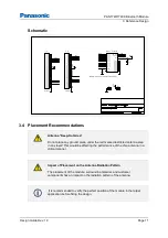
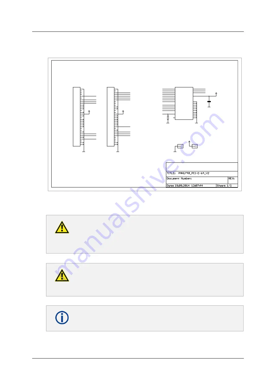
Schematic
3.4 Placement Recommendations
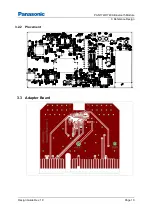
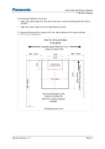
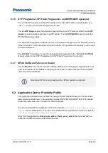
Antenna
“Keep-Out Area”
Do not place any ground plane under the red marked restricted antenna area
in any layer! This would be affecting the performance of the chip antenna in a
critical manner.
Impact of Placement on the Antenna Radiation Pattern
The placement of the module, surrounding material, and customer
components has an impact on the radiation pattern of the antenna.
It is recommended to verify the perfect position of the module in the target
application before fixing the design.
V
C
C
PCI-E-64
PCI-E-64
V
C
C
V
C
C
0.1
V
C
C
n
.c
./
0
VCC
8
VPP
14
SW_CLK
16
SW_DIO
18
P0.0
12
P0.1
11
P0.2
10
P0.3
9
P0.4
6
P0.5
5
P0.6
4
P0.7
3
P1.0
24
P1.1
23
P1.2
22
P1.3
21
N.C.
13
RST
2
GND
1
GND
7
GND
15
GND
17
GND
19
GND
20
GND
A
GND
B
GND
C
GND
D
MOD1
PAN1740
A1
A2
A3
A4
A5
A6
A7
A8
A9
A10
A11
A12
A13
A14
A15
A16
A17
A18
A19
A20
A21
A22
A23
A24
A25
A26
A27
A28
A29
A30
A31
A32
J1_A
B1
B2
B3
B4
B5
B6
B7
B8
B9
B10
B11
B12
B13
B14
B15
B16
B17
B18
B19
B20
B21
B22
B23
B24
B25
B26
B27
B28
B29
B30
B31
B32
J1_B
C1
R
1
1
JP1
1
JP2
P0.0
P0.0
P0.1
P0.1
P0.2
P0.2
P0.3
P0.3
P0.4
P0.4
P0.5
P0.5
P0.6
P0.6
P0.7
P0.7
P1.0
P1.0
P1.1
P1.1
P1.2
P1.2
P1.3
P1.3
RST
RST
VPP
VPP
SWCLK
SWCLK
SWDIO
SWDIO
Reset PIN resistor is not mounted if the module is empty


