background image


PAN9420 Wi-Fi Module 


3 PAN9420 Module 


Design Guide Rev. 1.0 


Page 10 


3.6  Placement 


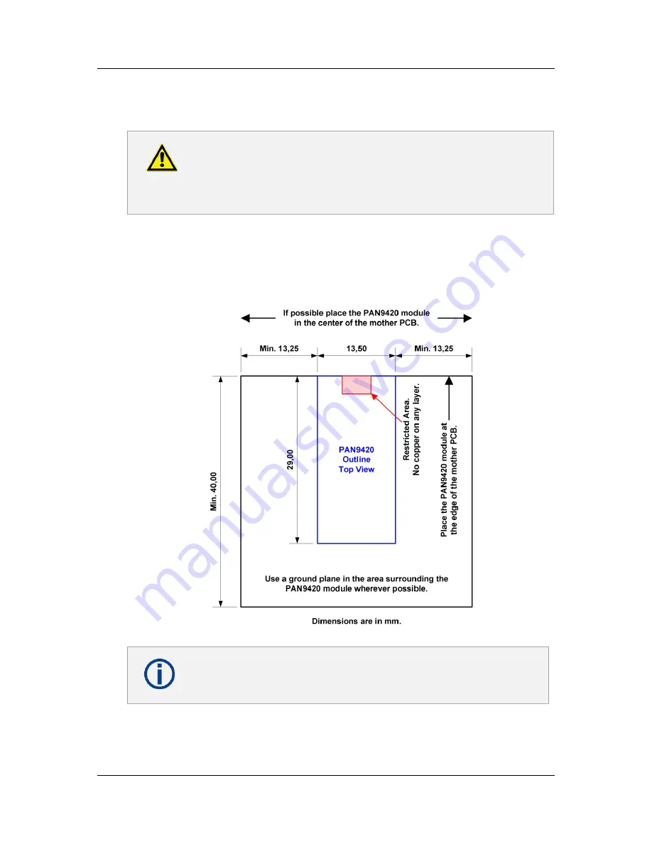
Antenna Keep-out Area 

Do not place any ground plane under the marked restricted antenna area in 
any layer! This would be affecting the performance of the chip antenna in a 
critical manner. 


The following requirements must be met: 


Keep this product away from heat. Heat is the major cause of decreasing the life of these 
products. 


Keep this product away from other high frequency circuits. 


The above recommendation for the ground plane is based on a FR4 4-Layer 
PCB. 


Summary of Contents for PAN9420

Page 1: ...PAN9420 Fully Embedded Stand Alone Wi Fi Module Design Guide Rev 1 0 Wireless Modules...

Page 2: ...and transparent data Integrated QSPI flash memory for customer web contents and configuration file Programming via standard JTAG Evaluation kit with pre installed web application for quick prototypin...

Page 3: ...have the status Engineering Samples This means that the design of this product is not yet concluded Engineering Samples may be partially or fully functional and they may differ from the published Prod...

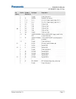
Page 4: ...5 Solder and Resist Mask 9 3 6 Placement 10 3 7 Power Supply 11 3 8 RF Path 11 4 PAN9420ETU Easy To Use 14 4 1 PAN9420ETU Live View 14 4 2 Functional Blocks 15 4 3 Pinning 16 4 4 Part Placement 18 4...

Page 5: ...e of Symbols Symbol Description Note Indicates important information for the proper use of the product Non observance can lead to errors Attention Indicates important notes that if not observed can pu...

Page 6: ...egrate our module PAN9420 in their product This Design Guide describes the hardware integration and gives useful hints This document is structured into two main parts The hardware integration of the P...

Page 7: ...dule 3 1 Block Diagram Chip Antenna SPDT 88MW300 MCU Radio SoC Crystal 32 768 kHz QSPI Flash 32 Mbit SPI UART0 UART1 GPIOs Status LEDs MCU Ready Resetn Factory Reset V SPDT Wake Ups JTAG Vcc 3 3 V LPF...

Page 8: ...QSPI D0 QSPI D1 NC NC WAKE UP1 QSPI CLK QSPI D3 NC BT FREQ BT GRANT BT REQ BT STATE NC NC NC NC 3 3V 3 3V UART1 CTSn UART1 RTSn UART1 TXD UART1 RXD QSPI CS2 GND STAT LED2 STAT LED1 STAT LED3 UART0 RXD...

Page 9: ...mm E1 E2 E3 E4 E5 D1 D2 D3 D4 D5 C1 C2 C3 C4 C5 B1 B2 B3 B4 B5 A1 A2 A3 A4 A5 2 3 4 5 6 7 8 9 10 11 12 13 14 35 34 33 32 31 30 29 28 27 26 25 24 23 5 0 mm Mother PCB edge 16 PCB footprint recommendati...

Page 10: ...area in any layer This would be affecting the performance of the chip antenna in a critical manner The following requirements must be met Keep this product away from heat Heat is the major cause of de...

Page 11: ...und of at least 47 F directly at the module The supply voltage should not be exceedingly high or reversed It should not carry noise and or spikes Make sure that the power up sequence meets the require...

Page 12: ...distances of the trace to the ground layers and the material of the PCB The following requirements shall be met Trace impedance of 50 Trace length shall not exceed 2 cm Via fence around the trace Cros...

Page 13: ...20 Module Design Guide Rev 1 0 Page 13 Example 2 50 Coplanar Waveguide with Ground and Micro Vias Trace width Trace distance to ground Substrate thickness Effective Permittivity Loss Tangent W 300 m S...

Page 14: ...No ENW49C01AZKF is a sample application of the PAN9420 module It is designed for mounting on the PAN9420 mother board Order No ENW49C01AYKF 4 1 PAN9420ETU Live View 4 1 1 PAN9420 Mother Board Live Vi...

Page 15: ...e Design Guide Rev 1 0 Page 15 4 2 Functional Blocks Functional Block Description A Vcc LED is active when Vcc is supplied B Reset button C Status LED s D PAN9420 module E On board antenna or U FL con...

Page 16: ...Y RESET Factory reset valid after 10 seconds active high 4 5 38 WAKE UP0 Wake up signal for MCU WLAN SoC active high 6 C3 WAKE UP1 Wake up signal for MCU WLAN SoC active high 7 8 9 UART1 CTS CTSn for...

Page 17: ...for JTAG 8 E3 TMS TMS for JTAG 9 D2 TRSTn TRSTn for JTAG 10 28 UART0 RXD DUAL SW RXD for UART0 UART1 toggle switch for the control of the state 11 27 UART0 TXD DUAL STAT TXD for UART0 UART1 state bina...

Page 18: ...dule 4 PAN9420ETU Easy To Use Design Guide Rev 1 0 Page 18 4 4 Part Placement MOD1 R6 R7 LED2 LED3 R8 R10 LED4 LED5 R2 R3 R4 R5 C1 R13 R9 C3 R15 LED6 R1 X2 X3 S1 JP1 JP2 LED1 R1 C2 S4 R2 R17 R18 R19 R...

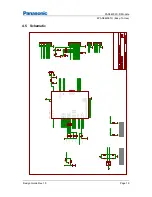
Page 19: ...GPIO 27 _ _BOOT2 6 GPIO 46 _ _SSP2_CLK 32 GPIO 47 _ _SSP2_FRM 31 STATUS_LED3 35 STATUS_LED2 34 STATUS_LED1 33 RESETN 37 WAKE_UP0 38 GPIO 48 _ _SSP2_TXD 30 MCU_READY 41 FACTORY_RESET 42 WAKE_UP1 C3 QS...

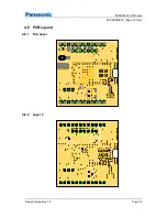
Page 20: ...PAN9420 Wi Fi Module 4 PAN9420ETU Easy To Use Design Guide Rev 1 0 Page 20 4 6 PCB Layout 4 6 1 Top Layer 4 6 2 Layer 2...

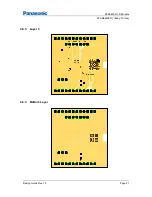
Page 21: ...PAN9420 Wi Fi Module 4 PAN9420ETU Easy To Use Design Guide Rev 1 0 Page 21 4 6 3 Layer 3 4 6 4 Bottom Layer...

Page 22: ...ld Design Guide Rev 1 0 Page 22 5 PAN9420 Arduino Shield The PAN9420 Arduino Shield Order No ENW49C01AXKF is a further sample application of the PAN9420 module It is designed for mounting on the Ardui...

Page 23: ...en Vcc is supplied D GPIO pins 4 5 of the PAN9420 module E IP connectivity pin allocated IP F Status LED s G MCU ready pin H Wake up 1 pin K Wake up 0 pin L JTAG Interface M Ground pins N General purp...

Page 24: ...e not used for this Arduino shield 5 4 Part Placement 1 2 20 GREEN GREEN YELLOW RED BLUE WHITE R5 R6 LED1 LED2 R7 R8 LED3 LED4 R13 R14 R15 R16 C4 R12 R2 C1 R1 LED5 C2 SV1 R4 R9 R11 R17 R18 R19 R20 LED...

Page 25: ...LED5 C2 SV1 1 3 5 7 9 11 13 15 17 19 2 4 6 8 10 12 14 16 18 20 R4 R9 R11 R17 R18 R19 R20 LED6 R21 1 JP1 1 JP2 1 JP3 1 JP4 1 JP5 1 JP6 1 JP7 1 JP8 1 JP9 1 JP10 1 JP11 1 JP12 1 JP13 1 JP14 1 JP15 1 JP16...

Page 26: ...PAN9420 Wi Fi Module 5 PAN9420 Arduino Shield Design Guide Rev 1 0 Page 26 5 6 PCB Layout 5 6 1 Top Layer 5 6 2 Bottom Layer...

Page 27: ...result in a significant personal injury to the user or as a critical component in any life support device or system whose failure to perform can be reasonably expected to cause the failure of the lif...

Page 28: ...Wi Fi module IEEE 802 11 b g n Regulatory notice ETSI for EU and other Supported channel Channel 1 13 2412 2472 MHz 500 ENW49C01AZKF PAN9420ETU PAN9420 Easy To Use pin header board with the module EN...

Page 29: ...sit the Panasonic Sales Support website to find assistance near you at https na industrial panasonic com distributors Please visit the Panasonic Wireless Technical Forum to submit a question at https...

Reviews: