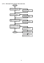
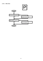
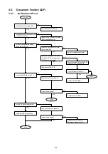
153
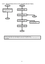
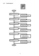
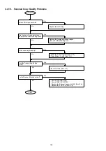
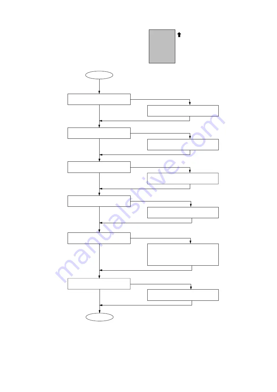
4.4.7.
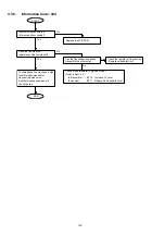
Dark Background
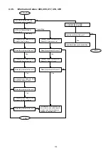
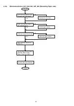
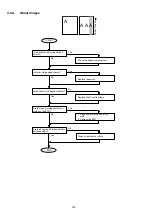
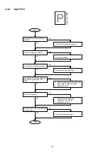
Is the LSU normal?
No
Yes
Replace the LSU.
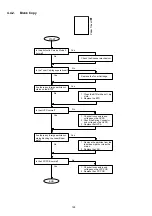
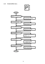
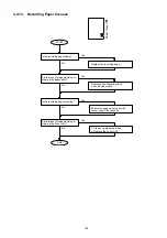
START
No
Yes
Is the printout in Service Mode 3
normal?
Check the Scanner mechanism.
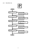
Is the Toner Cartridge operational?
No
Yes
Is the recording paper damp?
Yes
No
Replace the paper.
Replace the Toner Cartridge.
Is the HVPS normal?
1. Check all connectors and
voltages on the HVPS.
2. Check the Spring Connector
and voltage on the HVPS.
3. Replace the HVPS.
Yes
No
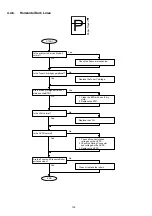
END
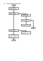
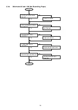
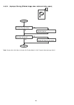
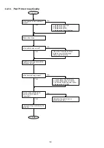
No
Yes
Clean or replace the rollers.
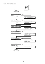
Paper Travel
P
Are the Fuser and Pressure Roller
surfaces clean?
Summary of Contents for Panafax DX-2000
Page 2: ......
Page 27: ...27 9 1 Screw 19 10 Release two Latch Hooks 11 Remove the SNS Assembly 121 9 10 11 ...
Page 49: ...49 2 15 Screw Identification Template ...
Page 57: ...57 3 7 3 Option Cassette Circuit 555 748 728 744 928 953 730 731 731 952 944 930 931 931 ...
Page 58: ...58 3 7 4 LAN Control Circuit 522 CN50 1102 1104 1101 N C N C RD N C N C RD TD TD ...
Page 59: ...59 3 7 5 Page Description Language Printer Interface Kit ...