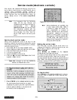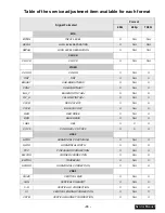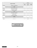
- 48 -
Service Manual
4.
Apply
the
following
signal
from
the
RF
signal generator:
Video: 100 IRE flat field, 30% modulation.
Audio: 3KHz, 30% modulation, stereo (left only).
(70dB ± 5dB, 75
Ω
OPEN, P/S 10dB).
Note: Set the 30% modulation with the P.L and
N.R. switches OFF then turn them ON while
testing.
5.
Adjust MTS High-Level Separation “SEPAH” DAC
data until the amplitude of the waveform measured
on the scope is minimum.
6.
Repeat above steps 2 through 5 until the amplitude
is at minimum for both signals.
Clock Adjustment (CLOCK)
Preparation:
Connect the frequency counter from IC001 MPU
Pin 10 or TPA009, to cold ground (
).
Note:
Frequency Counter probe capacitance should
be 8pF or less.
Procedure:
1.
Turn the PTV “ON” with the AC power applied.
2.
Measure TPA009 IC001 MPU pin 10 for frequency
and record the reading.
Note:
Pin 10 measurement must have at least four
digits of resolution following the decimal point.
Example: 000.0000
3.
Place the PTV into service mode for making
electronic adjustment, select the clock adjustment
DAC CLOCK and change value to 128.
4.
Calculate
and
set
CLOCK
based
on
the
following formula:
Note:
Pin
10
measurement
will
not
change
regardless of the value stored in CLOCK.
CLOCK
128
0.450x106x
732.422
p
Ð
in
10
( )
Hz
[
]
{
}
732.4220
------------------------------------------------------------
+
=
-
Summary of Contents for PT47WX52F - 47" PROJECTION TV HD
Page 65: ... 65 Notes PARTS LIST ...
Page 66: ... 66 D Board Schematic ...
Page 67: ... 67 D Board Schematic ...
Page 68: ... 68 D Board Schematic ...
Page 69: ... 69 Jumper between pin 7 and pin 1 D Board Schematic ...
Page 70: ... 70 D Board Schematic ...
Page 71: ... 71 D Board Schematic ...
Page 73: ... 73 NOTES NOTES ...
Page 74: ... 74 D Board Layout ...
Page 75: ... 75 D Board Layout ...
Page 76: ... 76 A Board Schematic ...
Page 77: ... 77 A Board Schematic ...
Page 78: ... 78 A Board Schematic ...
Page 79: ... 79 A Board Schematic ...
Page 80: ... 80 A Board Schematic ...
Page 81: ... 81 A Board Schematic ...
Page 82: ... 82 A Board Schematic ...
Page 83: ... 83 A Board Schematic ...
Page 84: ... 84 Board section Top A Board Layout Top left portion ...
Page 85: ... 85 Board section Top A Board Layout Top right portion ...
Page 86: ... 86 Board section Top A Board Layout Bottom left portion ...
Page 87: ... 87 Board section Top A Board Layout Bottom right portion ...
Page 88: ... 88 Board section Bottom side A Board Layout Top left portion ...
Page 89: ... 89 Board section Bottom A Board Layout Top right portion ...
Page 90: ... 90 Board section Bottom A Board Layout Bottom left portion ...
Page 91: ... 91 Board section Bottom A Board Layout Bottom right portion ...
Page 92: ... 92 LG Board schematic TNP2AA112 LG Board schematic ...
Page 94: ... 94 LR Board schematic TNP2AA111 LR Board schematic ...
Page 96: ... 96 LB Board schematic TNP2AA110 LB Board schematic ...
Page 98: ... 98 K Board schematic TNP2AA089 K Board layout TNP2AA089 K Board schematic and layout ...
Page 99: ... 99 G Board schematic TNP2AA090 G Board layout TNP2AA090 G Board schematic and layout ...
Page 104: ...Printed in USA K02042127PL0429 ...


