UNUSED ITEM NUMBERS
18, 19, 20, 27, 31, 32, 33, 34, 37, 39, 40, 46, 47, 48, 49,
52, 53, 60,
61, 65, 68, 72, 75, 76, 101, 102, 103, 104, 105, 106, 107,
110, 111,
113, 114, 115, 116, 117, 118, 119, 120, 121, 122, 123,
402, 407, 412,
417, 420, 426, 428, 432, 433, 436, 437, 438, 439, 441,
443, 445, 446,
448, 450, 451, 452, 453, 454, 457, 463, 464, 465, 466,
467, 468, 469,
470, 472, 473, 475, 476, 477, 478
8.2. ELECTRICAL REPLACEMENT PARTS LIST
USE ONLE ORIGINAL VIDEO REPLACEMENT PARTS LIST: To maintain original
FUNCTION and RELIABILITY of repaired units, use only ORIGINAL REPLACEMENT
PARTS which are listed with their part numbers in the parts list section of the Service
Manual.
Special Note:
All integrated circuits and many other semiconductor devices are electrostatically
sensitive and therefore require the special handling techniques described under the
"ELECTROSTATICALLY SENSITIVE (ES) DEVICES" Section of this service manual.
Note:
1. Be sure to make your orders of replacement parts according to this list.
2. IMPORTANT SAFETY NOTICE
Components identified by the sign have special characteristics important for
safety. When replacing any of these components, use only the specified parts.
3. Unless otherwise specified;
All resistors are in OHMS, 1/4W, +-5%, carbon, K=1,000 OHM, M=1,000K OHM.
All capacitors are in MICROFARADS(UF), P=UUF, +-10%. All coils are in
MICROHENRIES(UH), M=103UH, +-10%.
4. C.B.A.: Circuit Board Assembly.
5. P.C.B.: Printed Circuit Board.
6. E.S.D.: Electrostatically Sensitive Devices.
7. ITEM NUMBERS WITH CAPITAL LETTER E
Item numbers with capital letter E (Example: E1, E2,...) in the Ref. No. column are
128
Summary of Contents for PV-4601 A
Page 14: ...Fig 2 3 14 ...
Page 27: ...Fig 11 1 1 27 ...
Page 40: ...Fig D1 40 ...
Page 42: ...Fig D2 42 ...
Page 43: ...Fig D3 43 ...
Page 44: ...Fig D4 44 ...
Page 45: ...Fig D5 45 ...
Page 46: ...Fig D7 46 ...
Page 47: ...Fig D8 47 ...
Page 51: ...Fig M2 1 Fig M2 2 51 ...
Page 53: ...Fig M4 1 53 ...
Page 77: ...Fig M19 77 ...
Page 84: ...Fig J5 84 ...
Page 85: ...Fig J6 85 ...
Page 87: ...Fig J9 87 ...
Page 88: ...Fig J10 88 ...
Page 89: ...Fig J11 89 ...
Page 90: ...Fig J12 90 ...
Page 91: ...Fig J13 91 ...
Page 92: ...Fig J15 92 ...
Page 93: ...93 ...
Page 96: ...96 ...
Page 102: ...with the holes on the Pinch Lift Cam as shown in Fig A6 102 ...
Page 103: ...103 ...
Page 105: ...Fig K1 105 ...
Page 106: ...Fig K2 106 ...
Page 107: ...Fig K3 107 ...
Page 109: ...Fig B1 109 ...
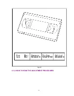
Page 114: ...Fig E1 4 3 2 HOW TO READ THE ADJUSTMENT PROCEDURES 114 ...
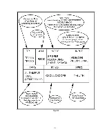
Page 115: ...Fig E2 115 ...
Page 134: ...R6004 ERJ6GEYJ333V MGF CHIP 1 10W 33K 134 ...
Page 136: ...R6085 ERJ6GEYJ223V MGF CHIP 1 10W 22K 136 ...
Page 140: ...C4601 ECEA1CKA100 ELECTROLYTIC 16V 10 140 ...
Page 147: ...R6065 ERJ6GEYJ223V MGF CHIP 1 10W 22K 147 ...
Page 167: ...9 11 Operation Block Diagrams 1 167 ...
Page 178: ......
Page 204: ......
Page 205: ......


