shown in the exploded views. The E item numbers are also printed on the same
page at the top of the column.
8. The parts with "
Û
" mark are supplied individually or as a unit.
The parts with "
ÛÛ
" mark are supplied individually or as a unit, and are included in
"
Û
" parts listed directly above in the parts list.
9. RTL: Retention Time Limited
This indicates that the retention time is limited for this item. After the
discontinuation of this item in production, it will no longer be available.
10. NR: Non Repairable Board Ass'y
11. SERVICE OF CHIP PARTS
When servicing chip parts, please use a soldering iron of less than 30 watts.
Refer to "IC, TRANSISTOR AND CHIP PART INFORMATION" page.
12. List of Abbreviations for Part Names & Descriptions:
MGF CHIP: METAL GLAZE FILM CHIP
C CHIP: CERAMIC CHIP
COMPLX CMP: COMPLEX COMPONENT
W FLMPRF: WIREWOUND FLAMEPROOF
13. The parts with "•" are 0 OHM resistor. When replacing, a wire can be
substituted for a 0 OHM resistor.
14. Parts different in shape or size may be used. However, only interchangeable
parts will be supplied as service replacement parts.
Model: D, E
Hi-Fi Audio C.B.A. replacements note:
The following parts on the Hi-Fi Audio C.B.A. (VEPS4003A1) is not supplied
separatery. Please order and replace with the circuit board assembly instead of
individual parts.
IC4201 R4223 R4224 R4225 R4226 R4227 R4236
Model: B
Power supply C.B.A. replacements note:
VEPS1002B2 or VEPS01046G2 is used for Power supply C.B.A.. However, for parts
standardization, VEPS1002B2 will be supplied as a replacement for this model.
Please note that VEPS1002B2 and VEPS01046G2 are interchangeable. Only
129
Summary of Contents for PV-4601 A
Page 14: ...Fig 2 3 14 ...
Page 27: ...Fig 11 1 1 27 ...
Page 40: ...Fig D1 40 ...
Page 42: ...Fig D2 42 ...
Page 43: ...Fig D3 43 ...
Page 44: ...Fig D4 44 ...
Page 45: ...Fig D5 45 ...
Page 46: ...Fig D7 46 ...
Page 47: ...Fig D8 47 ...
Page 51: ...Fig M2 1 Fig M2 2 51 ...
Page 53: ...Fig M4 1 53 ...
Page 77: ...Fig M19 77 ...
Page 84: ...Fig J5 84 ...
Page 85: ...Fig J6 85 ...
Page 87: ...Fig J9 87 ...
Page 88: ...Fig J10 88 ...
Page 89: ...Fig J11 89 ...
Page 90: ...Fig J12 90 ...
Page 91: ...Fig J13 91 ...
Page 92: ...Fig J15 92 ...
Page 93: ...93 ...
Page 96: ...96 ...
Page 102: ...with the holes on the Pinch Lift Cam as shown in Fig A6 102 ...
Page 103: ...103 ...
Page 105: ...Fig K1 105 ...
Page 106: ...Fig K2 106 ...
Page 107: ...Fig K3 107 ...
Page 109: ...Fig B1 109 ...
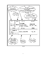
Page 114: ...Fig E1 4 3 2 HOW TO READ THE ADJUSTMENT PROCEDURES 114 ...
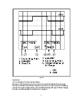
Page 115: ...Fig E2 115 ...
Page 134: ...R6004 ERJ6GEYJ333V MGF CHIP 1 10W 33K 134 ...
Page 136: ...R6085 ERJ6GEYJ223V MGF CHIP 1 10W 22K 136 ...
Page 140: ...C4601 ECEA1CKA100 ELECTROLYTIC 16V 10 140 ...
Page 147: ...R6065 ERJ6GEYJ223V MGF CHIP 1 10W 22K 147 ...
Page 167: ...9 11 Operation Block Diagrams 1 167 ...
Page 178: ......
Page 204: ......
Page 205: ......


