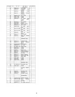

16
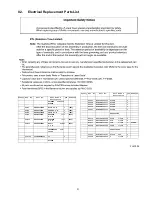
6.2.
MAIN CIRCUIT (2/6)
15
16
17
18
19
20
21
22
23
24
25
26
27
28
B
MAIN CIRCUIT
SCHEMATIC DIAGRAM - 3
RX-D55EE MAIN CIRCUIT
2/6
3/6
5/6
1/6
4/6
6/6
TO MAIN
SECTION (1/6)
TO MAIN
SECTION (5/6)
TO MAIN
SECTION (3/6)
P1
2
4
3
1
P1
AA
P1
AB
D
TO
PANEL CIRCUIT
(ZJ903*)
IN SCHEMATIC
DIAGRAM - 9
: FM/AM SIGNAL LINE
: FM SIGNAL LINE
: +B SIGNAL LINE
: AM SIGNAL LINE
: MUSIC PORT AUDIO INPUT SIGNAL LINE
: AUDIO OUTPUT SIGNAL LINE
: CD/TAPE AUDIO INPUT SIGNAL LINE
5
10K
R4159
10K
R4158
L4108
J0JBC0000019
L4107
J0JBC0000019
L4106
J0JBC0000019
R4156
220
R4157
220
7
6
3
2
4
1
5
JK4101
PHONES
C4146
16V10
C4154
25V3300
C4187
25V2200
PGND
FP4100
5A
C4145
25V100
C4185
16V10
C4186
16V10
DGND
TUNER_GND
MUTE_A
M+9VGND
2
1
4
3
CN4104
R-
R+
L+
L-
13
8
5
1
2
3
4
6
7
9
10
11
12
14
IC4101
C1BA00000420
POWER AMPLIFIER
R4165
4.7K
C4120
16V47
2.2
R4143
0
R4126
R4146
2.2
C4143
2700P
C4144
2700P
C4157
0.22
R4148
2.2
C4163
0.22
C4156
0.22
2.2
R4147
C4161
0.22
12VCC
STDBY
12VCC
PWRGND
LCH_IN
LOUT(+)
LOUT(-)
PWRGND
ROUT(+)
ROUT(-)
RCH_IN
RIP_FIL
PRE_GND
SIGNAL
MUTE
0.1
C4152
R4161
22K
R4162
22K
2
3
1
5
4
6
MUTING
B1HBECA00004
Q4109
Summary of Contents for RX-D55EE
Page 14: ...14 ...