background image

100 mA (FM & AM)
180 mA (FM REC & AM REC)
150 mA (TAPE Playback)
240 mA (CD)
290 mA (CD REC)
Volume maximum :
300 mA (FM & AM)
380 mA (FM REC & AM REC)
440 mA (TAPE Playback)
590 mA (CD)
690 mA (CD REC)

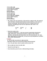
The voltage value and waveforms are the reference voltage of this unit measured 

by DC electronic voltmeter (high impedance) and oscilloscope on the basis of 
chassis. Accordingly, there may arise some error in voltage values and 
waveforms depending upon the internal impedance of the tester or the 
measuring unit.

No mark

...Playback

< >

...FM

(( ))

...CD

( )

...AM

Importance safety notice:

Components identifed by    mark have special characteristics important for 
safety. Furthermore, special parts which have purposes of fire-retardant 
(resistors), high-quality sound (capacitors), low-noise (resistors), etc. are used. 
When replacing any of components, be sure to use only manufacturer’s specified 
parts shown in the parts list.

Caution!

IC, LSI and VLSI are sensitive to static electricity.
Secondary trouble can be prevented by taking care during repair.

Cover the parts boxes made of plastics with aluminium foil.

Put a conductive mat on the work table.

Ground the soldering iron.

Do not touch the pins of IC, LSI or VLSI with fingers directly.

25

Summary of Contents for RXD10 - RADIO CASSETTE W/CD

Page 1: ...Order No MD0105085C1 A6 Portable Stereo CD System RX D10 Color A Blue Type PC Canada Tape Deck SG20 Mechanism Series Traverse Deck RAE0152Z 1C Traverse Deck Series SPECIFICATIONS 1 ...

Page 2: ... pole magnet Monitor system Variable sound monitor Frequency range Normal position 50 Hz 12 kHz CD PLAYER Sampling frequency 44 1 kHz Decoding 16 bit linear Beam source Semiconductor laser wavelength 780 nm No of channels 2 channel stereo Wow and flutter Less than possible measurement data D A converter MASH 1 bit DAC GENERAL Power Requirement AC 120 V 60 Hz Battery 9 V six R20 LR20 D UM 1 batteri...

Page 3: ... power discharge Power Supply Capacitors C120 C220 C317 through a 10 5 W resistor to ground DO NOT SHORT CIRCUIT DIRECTLY with a screw driver blade for instance as this may destroy solid state devices After repairs are completed restore power gradually using a variac to avoid over current Current consumption at AC 120 V 60 Hz in NO SIGNAL mode should be 75 mA respectively 2 Protection Circuitry Th...

Page 4: ...s follow the procedure outlines below 1 Turn off the power 2 Determine the cause of the problem and correct it 3 Turn on the power once again after one minute Note When the protection circuitry functions the unit will not operate unless the power is first turned off and then on again 3 Accessories AC power cord Battery Service Life UM 1 D size Batteries Approximately 28 hrs of Tape Recording EIAJ ...

Page 5: ...g pin is inserted into the flexible board FFC board 3 Take care not to apply excessive stress to the flexible board FFC board When removing or connecting the short pin finish the job in as short time as possible 4 Do not turn the variable resistor laser power adjustment It has already been adjusted Grounding for electrostatic breakdown prevention 1 Human body grounding Use the anti static wrist st...

Page 6: ...6 ...

Page 7: ...set variable resistor on the pickup lens 4 Do not disassemble the optical pickup unit 5 If the optical pickup is replaced use the manufacturer s specified replacement pickup only 6 Use of control or adjustments or performance of procedures other than those specified herein may result in hazardous radiation exposure CAUTION THIS PRODUCT UTILIZES A LASER USE OF CONTROLS OR ADJUSTMENTS OR PERFORMANCE...

Page 8: ...6 Controls 8 ...

Page 9: ...9 ...

Page 10: ...tic mode 3 At the state of T display operate as follows Open the CD lid and close it right away Start recording TAPE and STOP it at once 4 Press CLEAR key Self diagnostic results i e the memorized errors during actual operations and the result of above mentioned operation shall be displayed alternately If there is no error the aforementioned display T shall be kept If the operation in the above me...

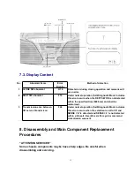
Page 11: ...the specified time 5000 ms and shall be memorised 3 Transmission error between CD servo LSI and micon F26 Under normal operation Self Diagnostic Mode inclusive this error occurs when the selection is set to CD and SENSE H is detected and SENSE L is not detected within a fail safe time 20 ms after system command transmission was sent 8 Disassembly and Main Component Replacement Procedures ATTENTION...

Page 12: ... required 4 Refer the Parts No on the page of Main component Replacement Procedures if necessary Content Disassembly Procedure for each major P C B 1 ing for the Main Panel1 Panel2 Speaker Terminal P C B P g 7 8 2 Checking for the CD Servo P C B P g 8 Main Component Replacement Procedures 1 Replacement of the Traverse Deck P g 9 2 Installation of the CD Servo P C B after Replacement P g 10 Warning...

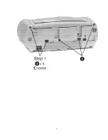
Page 13: ...13 ...

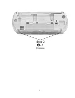
Page 14: ...14 ...

Page 15: ...15 ...

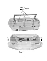
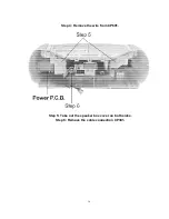
Page 16: ...Step 4 Remove the wire from CP601 Step 5 Take out the speaker box cover on both sides Step 6 Remove the cable connection CP301 16 ...

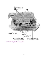
Page 17: ...8 1 2 Checking for CD Servo P C B 17 ...

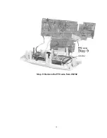
Page 18: ...Step 9 Remove the FFC wire from CN702 18 ...

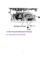
Page 19: ...8 2 Main Component Replacement Procedures 8 2 1 Replacement of the Traverse Deck 19 ...

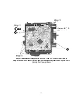
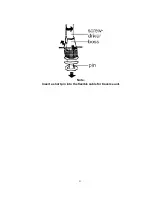
Page 20: ...Step 2 Desolder the 4 legs of the 2 motors and pull out the Servo P C B Step 3 Widen the 3 bosses with a flat screwdriver and pull out the 3 pins Then remove the Traverse Deck 20 ...

Page 21: ...Note Insert a short pin into the flexible cable for traverse unit 21 ...

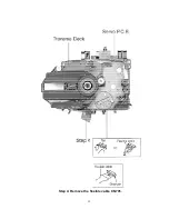
Page 22: ...Step 4 Remove the flexible cable CN701 22 ...

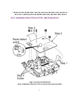
Page 23: ...tor in the direction of the arrow 1 and the pull out the flexible cable in the direction of the arrow 2 8 2 2 Installation of the CD Servo P C B after Replacement Step 1 Connect the FFC board Step 2 Install the CD servo P C B in the traverse deck assembly 23 ...

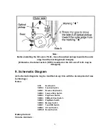
Page 24: ... 9 Schematic Diagram All schematic diagrams may be modified at any time with the development of new technology Notes S701 Rest Switch SW302 Function Switch SW601 Reverse Skip Switch SW602 Forward Skip Switch SW603 Play Pause Switch SW604 FM Mode Clear Switch SW605 Play Mode Switch SW606 Memory Switch SW607 Tone XBS Switch SW802 CD Leaf Switch SW1001 Record Switch Battery Current Volume minimum 24 ...

Page 25: ... mark Playback FM CD AM Importance safety notice Components identifed by mark have special characteristics important for safety Furthermore special parts which have purposes of fire retardant resistors high quality sound capacitors low noise resistors etc are used When replacing any of components be sure to use only manufacturer s specified parts shown in the parts list Caution IC LSI and VLSI are...

Page 26: ...26 ...

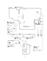
Page 27: ...10 Printed Circuit Board 11 Wiring Connection Diagram 27 ...

Page 28: ...28 ...

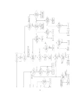
Page 29: ...12 Troubleshooting Guide 29 ...

Page 30: ...30 ...

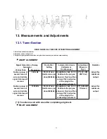
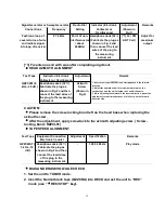
Page 31: ...turns of wire and radiate signal into loop of receiver 540 kHz Point of non interference on about 600kHz Headphone Jack 32 Fabricate the plug as shown in Fig 2 and then connect the lead wires of the plug to the measuring instrument 1 L3 AM ANT Coil Adjust for maximum output Fashion a loop of several turns of wire and radiate signal into loop of receiver 1400 kHz Point of non interference on about ...

Page 32: ...Screw Shown in Fig 3 1 Insert a test tape QZZCFM and start playback in the forward direction 2 Adjust the azimuth screw for maximum waveform on the oscilloscope and the similar output on L and R channels 3 When adjusting the azimuth in the reverse direction repeat the adjustment several times because of a little slip on the forward direction side CAUTION Please remove the screw locking bond left o...

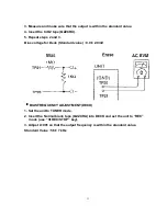
Page 33: ...eps 2 and 3 Bias voltage for Deck Standard value 9 0 2 0mV BIAS FREQUENCY ADJUSTMENT DECK 1 Set the unit to TUNER mode 2 Insert the Normal blank tape QZZCRA into DECK and set the unit to REC mode use REC STOP key 3 Adjust L1001 so that the output frequency is within the standard value Standard Value 56 7 kHz 33 ...

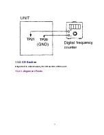
Page 34: ...13 2 CD Section Alignment is unneccessary for CD section of this unit 13 2 1 Alignment Points 34 ...

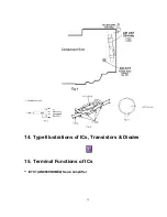
Page 35: ...14 Type Illustrations of ICs Transistors Diodes 15 Terminal Functions of ICs IC701 AN8839NSBE2 Servo Amplifier 35 ...

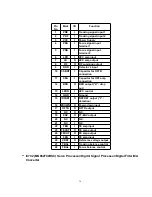
Page 36: ...Capacitor for HPF amp connection 12 BDO O BDO output H drop out 13 LDON I APC control 14 GND Ground 15 RFDET O NRFDET output L detection 16 PDOWN O Power down input 17 OFTR O OFTR output 18 NC O N C 19 ENV O 3T ENV output 20 NC I N C 21 NC I N C 22 TEN I TE amp input 23 TEOUT O TE amp output 24 FEOUT O FE amp output 25 FEN I FE amp input 26 VREF O Reference voltage output 27 TBAL I Tracking balanc...

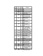
Page 37: ...nput 10 SENSE O Sense signal output OFT FESL MAGEND NAJEND POSAD SFG Not used open 11 FLOCK O Focus servo feeding signal output L Feed 12 TLOCK O Tracking servo feeding signal output L Feed 13 BLKCLK O Sub code block clock signal output 14 SQCK I External clock signal input for sub code Q resistor 15 SUBQ O Sub code Q code output 16 DMUTE I Muting input H Mute 17 STAT O Status signal output CRC CU...

Page 38: ...22 TVD O Traverse drive output 38 ...

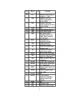
Page 39: ...AL O Tracking balance adjustment output 32 FE I Focus error signal input analog input 33 TE I Tracking error signal input analog input 34 RFENV I RF envelope signal input 35 VDET I Vibration detection signal input H detection 36 OFT I Off track signal input H off track 37 TRCRS I Track cross signal input 38 RFDET I RF detection signal input L detection 39 BDO I Dropout signal input H Dropout 40 LD...

Page 40: ...al mode must use other circuit 55 SUBC N C 56 SBCK I Clock input for sub code serial data 57 VSS I Gnd 58 X1 I Crystal oscillating circuit input f 16 9344MHz 59 X2 O Crystal oscillating circuit output f 16 9344MHz 60 VDD I Power supply input for oscillating circuit 61 BYTCK N C 62 CLDCK N C 63 FCLK N C 64 IPFLAG N C 65 FLAG N C 66 CLVS N C 67 CRC N C 68 DEMPH N C 69 RESY N C 70 IOSEL I Mode Switch...

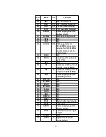
Page 41: ...il Tracking Coil Traverse Motor Spindle Motor Driver Pin No Mark I O Function 1 RST N C 2 NC N C 3 IN2 I Motor Drive 2 input 4 PC2 I Turn table motor drive signal L ON 5 NC N C 6 IN1 I Motor Driver 1 input 7 NC I N C 8 PVCC1 I Power supply 1 for driver 9 PGND1 Ground connection 1 for driver 10 NC N C 11 D1 O Motor driver 1 reverse action output 12 D1 O Motor driver 1 forward action output 13 D2 O ...

Page 42: ...r 3 input 27 RSTIN I Reset terminal 28 NC N C IC801 M38224M6H104 Microprocessor Pin No Mark I O Function 1 VLCD2 LCD power source 2 VLCD1 LCD power source 3 KEY_1 A D Key 1 input 4 REM_CTL O Control on off of remote sensor 5 REG_2 A D Region setting 2 6 REG_1 A D Region setting 1 7 R_CTL O Region control 8 P DET A D Power detect input 9 REG_3 I Region setting 3 10 N C N C 11 CD_SEL I CD mode selec...

Page 43: ...N 4 19MHz ceramic OSC input 31 OSC OUT 4 19MHz ceramic OSC output 32 VSS GND 33 MBP1 O Microcomputer beatproof control 1 34 MBP2 O Microcomputer beatproof control 2 35 MUTE_A O Audio mute 36 PLL DO I PLL if count input 37 CLOSE_SW I CD close detect SW 38 STAT I CD status input 29 CD RESET O CD RST output 30 REST_SW I CD limit SW input for the most inner point 41 MCLK O CD signal processor control ...

Page 44: ...rtant safety notice Components identified by mark have special characteristics important for safety Furthermore special parts which have purposes of fire retardant resistors high quality sound capacitors low noise resistors etc are used When replacing any of these components be sure to use only manufacturers s specified parts shown in the parts list The parenthesized indications in the Remarks col...

Page 45: ... with the lows govening part and product retention After the end of this period the assembly will no longer be available M indicates in the Remarks columns indicates parts that are supplied by MESA The SF mark denotes the standard part Reference for O I book languages are as follows Ar Arabic Cf Canadian French Cz Czech Da Danish Du Dutch En English Fr French Ge German It Italian Ko Korean Po Poli...

Page 46: ...071 1 SWING LEVER M 122 RML0072 1 AS RELEASE LEVER M 123 RML0073 1 AS PROTECT LEVER M 124 RML0074 1 IDLER LEVER M 125 RML0076 EJECT SELECTION LEVE M 126 RML0077 1 LOCK PLATE M 127 RML0078 FUNCTION PLATE M 128 XTN2 4F EARTH LUG SCREW M 129 RML0081 2 RECORD SAFETY LEVER M 130 RML0082 PAUSE LEVER M 131 RMM0023 1 PLAY ROD M 132 RMM0024 REW ROD M 133 RMM0025 FF ROD M 134 RMM0026 STOP ROD M 135 RMM0027 ...

Page 47: ...8 RHD26002 MOTOR SCREW M 159 XTN2 8F R P SCREW M 160 RMG0102 1 MOTOR RUB CUSHION M 162 RFM179ZA DC MOTOR ASS Y M 163 RMA0108 MOTOR BK M 164 XTN26 8J MOTOR BK SCREW M 165 RME0098 2 E SLIDE LEVER SPRING M 166 RJR0033 EARTH LUG M 167 RML0080 ERASE HEAD ARM M 168 RSH1A006 U LEAF SWITCH M 16 2 Cabinet CD Loading Mechanism 16 2 1 Cabinet CD Loading Machanism Parts Location 16 2 2 Cabinet CD Loading Mach...

Page 48: ...G M 19 RMA1007 SHIELD PLATE M 20 RMB0509 SPRING CD BUTTON M 21 RDG0288 DUMPER GEAR M 22 RMCX0018 RECORD SPRING M 24 RMNX0032A LCD HOLDER M 25 RMVX0050 SPEAKER BOX COVER M 26 RMVX0051 SPEAKER BOX COVER R M 27 RKQX0010 S TOP CABINET M 28 SUX102 REVOLVING ROD M 29 RFKNXDT39GCK CD HOLDER ASS Y M 30 RJC511XB BATT SPRING M 31 RJC70031ZC BATT SPRING M 32 RJCX0005 BATT TERMINAL M 33 RJRX0006 UN3 TERMINAL ...

Page 49: ...AVERSE CHASSIS M 362 RMS0627 FIXED PIN B M 363 XTN2 6G SCREW M 364 RMS0350 FIXED PIN A M 16 3 Components Parts List Ref No Part No Part Name Description Remarks P C B REP2880A N CD SERVO P C B M RTL REPX0196G MAIN TUNER P C B PANEL 1 P C B PANEL 2 P C B SPEAKER TERMINAL P C B BATTERY P C B POWER P C B M RTL INTEGRATED CIRCUITS IC1 TA2008AN IC TUNER M IC2 LC72131D U IC PLL M IC302 S81252SGY Z IC 5 ...

Page 50: ...TRANSISTOR M Q811 RVTDTC143EST DIGITAL TRANSISTOR M Q813 RVTDTC143EST DIGITAL TRANSISTOR M Q1001 KTC3199BLTA TRANSISTOR M DIODES D1 KV1520ATS2 VARICAP M D2 KV1360NTM VARICAP M D3 KV1360NTM VARICAP M D301 RVD1SS133TA SWITCHING DIODE M D302 RB441QT 77 DIODE M D303 RVD1SS133TA SWITCHING DIODE M D304 MTZJ7R5CTA ZENER DIODE M D305 RVD1SS133TA SWITCHING DIODE M D306 RVD1SS133TA SWITCHING DIODE M D307 RV...

Page 51: ...NNECTOR M CP301 RJP3G9YA 3P CONNECTOR M CP303 RJP4G18ZA TAPE HERD CONNECTOR M CP601 RJP3G9YA 3P CONNECTOR M TRIMMER CT1 RCVFMA10T01S TRIMMER CAPACITOR M COILS TRANSFORMERS L2 RLQY30S1W F FM COIL M L3 RLV2C046 0 FERRITE ANT M L4 RLD4Y45 F FM OSC COIL M L6 RL02B131 T AM OSC COIL M L7 RLQA101KT G INDUCTOR M L8 RLQY30S1W F FM COIL M L801 RLQA2R2KT G INDUCTOR M L819 RLQA2R2KT G INDUCTOR M L1001 RL09B17...

Page 52: ...7TK09 JK HEADPHONE M JK501 RJJ1SM02 X JK AC INLET SW501 M WIRES W301 REXX0218 TRANSFORMER TO MAIN M W302 RWJ9003220SS MAIN TO SPEAKER WIRE M W307 REXX0221 PANEL TO MAIN WIRE M W401 RWJ9002080SS RANEL TO PANEL WIRE M W501 RWJ8902170SS POWER TO BATT WIRE M W502 REU08H240QS POWER TO BATT WIRE M RESISTORS R2 ERDS2TJ103T 10K 1 4W M R3 ERDS2TJ332T 3 3K 1 4W M R4 ERDS2TJ472T 4 7K 1 4W M R5 ERDS2TJ221T 22...

Page 53: ... M R114 ERDS2TJ562T 5 6K 1 4W M R115 ERDS2TJ472T 4 7K 1 4W M R116 ERDS2TJ102T 1K 1 4W M R117 ERDS2TJ471T 470 1 4W M R123 ERDS2TJ472T 4 7K 1 4W M R125 ERDS2TJ680T 68 1 4W M R127 ERDS2TJ181T 180 1 4W M R140 ERDS2TJ102T 1K 1 4W M R208 ERDS2TJ562T 5 6K 1 4W M R210 ERDS2TJ682T 6 8K 1 4W M R211 ERDS2TJ562T 5 6K 1 4W M R213 ERDS2TJ183T 18K 1 4W M R214 ERDS2TJ562T 5 6K 1 4W M R215 ERDS2TJ472T 4 7K 1 4W M ...

Page 54: ...V 4 7 1 10W M R702 ERJ6GEYJ103V 10K 1 10W M R704 ERJ6GEYJ102V 1K 1 10W M R705 ERJ6GEYJ154V 150K 1 10W M R706 ERJ6GEYJ102V 1K 1 10W M R707 ERJ6GEYJ393V 39K 1 10W M R708 ERJ6GEYJ223V 22K 1 10W M R709 ERJ6GEYJ683V 68K 1 10W M R711 ERJ6GEYJ823V 82K 1 10W M R712 ERJ8GEYJ221V 220 1 8W M R714 ERJ6GEY0R00V 0 1 10W M R715 ERJ6GEYJ102V 1K 1 10W M R717 ERJ6GEYJ102V 1K 1 10W M R718 ERJ6GEYJ102V 1K 1 10W M R72...

Page 55: ...K 1 4W M R833 ERDS2TJ103T 10K 1 4W M R834 ERDS2TJ103T 10K 1 4W M R835 ERDS2TJ103T 10K 1 4W M R837 ERDS2TJ333T 33K 1 4W M R838 ERDS2TJ473T 47K 1 4W M R839 ERDS2TJ474T 470K 1 4W M R841 ERDS2TJ102T 1K 1 4W M R842 ERDS2TJ102T 1K 1 4W M R843 ERDS2TJ102T 1K 1 4W M R845 ERDS2TJ102T 1K 1 4W M R846 ERDS2TJ472T 4 7K 1 4W M R847 ERDS2TJ103T 10K 1 4W M R848 ERDS2TJ472T 4 7K 1 4W M R849 ERDS2TJ472T 4 7K 1 4W M...

Page 56: ...JC5 10 50V M C12 ECBT1H331KB5 330 50V M C13 ECA1CM100B 10 16V M C14 ECBT1H102KB5 1000P 50V M C15 ECFR1C683MR 0 068 16V M C16 ECFR1C823MR 0 082 16V M C17 ECFR1C823MR 0 082 16V M C18 RCQB2A273KTM 0 027 100V M C19 RCQB2A273KTM 0 027 100V M C20 RCE1HM010BP 1 50V M C21 RCE1HM010BP 1 50V M C22 ECA1HM4R7B 4 7 50V M C23 ECFR1C333MR 0 033 16V M C24 ECFR1C333MR 0 033 16V M C30 ECBT1H331KB5 330 50V M C31 ECB...

Page 57: ...0 015 16V M C140 ECBT1H102KB5 1000P 50V M C209 ECA1HM0R1B 0 1 50V M C210 RCE1HMR22BP 22 50V M C212 RCE1HM2R2BP 2 2 50V M C213 ECBT1H560J5 56 50V M C215 RCE1HM010BP 10 50V M C216 ECBT1H102KB5 1000P 50V M C217 ECA1AM101B 100 10V M C218 ECA1AM101B 100 10V M C220 ECA1AM471B 470 10V M C221 ECBT1H102KB5 1000P 50V M C225 RCQB2A104KM 0 1 100V M C230 ECFR1C153MR 0 015 16V M C240 ECBT1H102KB5 1000P 50V M C3...

Page 58: ... 820P 50V M C717 ECUVNE104ZFN 0 1 25V M C718 ECUVNC224KBN 0 22 16V M C721 ECUV1H100DCN 10P 50V M C722 ECUV1H100DCN 10P 50V M C723 ECEA1AKA221I 220 10V M C724 ECUVNE104MBN 0 1 25V M C725 ECUV1H102KBN 1000P 50V M C726 ECUV1H102KBN 1000P 50V M C727 ECEA1HPK010I 1 50V M C728 ECEA1HPK010I 1 50V M C730 ECUVNE104ZFN 0 1 25V M C731 ECEA0JKA221I 220 6 3V M C732 ECEA0JKA221I 220 6 3V M C733 ECUVNE104MBN 0 1...

Page 59: ... ECBT1H470J5 47 50V M C846 ECBT1H470J5 47 50V M C847 ECBT1H102KB5 1000P 50V M C858 ECBT1C103MS5 0 01 16V M C859 ECBT1H102KB5 1000P 50V M C864 ECBT1H102KB5 1000P 50V M C870 ECBT1H102KB5 1000P 50V M C871 ECBT1H561KB5 560 50V M C900 ECA1EM470B 47 25V M C1001 RCQB2A392KM 3900P 100V M C1002 ECA1AM101B 100 10V M C1003 ECBT1C682MR5 3800P 16V M C1004 ECBT1H102KB5 1000P 50V M C1006 RCE1HM2R2BP 2 2 50V M C1...

Page 60: ...EY0R00V 0 1 10W M RJ724 ERJ6GEY0R00V 0 1 10W M RJ727 ERJ6GEY0R00V 0 1 10W M RJ728 ERJ6GEY0R00V 0 1 10W M RJ731 ERJ6GEY0R00V 0 1 10W M RJ732 ERJ6GEY0R00V 0 1 10W M RJ734 ERJ6GEY0R00V 0 1 10W M RJ750 ERJ6GEY0R00V 0 1 10W M TEST JUMPER TJ701 EYF8CU TEST JUMEPR M 16 4 Packing Materials Accessories Parts List Ref No Part No Part Name Description Remarks PACKING MATERIALS P1 RPGX0807 GIFT BOX M P2 RPNX0...

Page 61: ...A2 O I BOOK Printed in Singapore M010500001FLE H C D J 1 2001 Matsushita Electronics S Pte Ltd All rights reserved Unauthorized copying and distribution is a violation of law 61 ...

Page 62: ... KV1520ATS2 S81252SGY Z PST9123T 1 2 3 S1NB20 4101 BA3313L 2SB709STX KTA1046 RVD1SS133TA RB441QT 77 MTZJ5R1BTA MTZJ6R2CTA MTZJ7R5CTA MTZJ18BTA 2SA1515STPQ MN662790RSC 80P M38224M6H104 100P RVTDTC143EST KTA12710YTA KV1360NTM 1 KRA102MTA KRC104MTA KTC3199BLTA KTC3199GRTA ...

Page 63: ...7 J503 J414 J413 J419 J400 J301 J300 1 19 J418 Q811 R852 R848 R851 Q810 R849 R846 Q813 C121 C221 C858 R831 R832 R833 R834 R821 J205 R835 R847 R822 J208 J408 J409 J328 J209 J410 J600 J411 R839 Q806 J502 C802 C804 R837 C835 KEY_1 GND J341 J340 J338 J332 J333 J324 J325 J311 J317 L801 J214 C859 J107 J102 J105 J123 J122 J128 J138 J146 J149 J133 J135 J144 J158 J159 J320 J127 J124 J125 J167 J164 J215 J16...

Page 64: ...00 J301 J300 Q811 R852 R848 R851 Q810 R849 C121 C221 R802 J202 J201 R801 C858 R831 R832 R833 R834 R821 R835 R847 J209 R808 Q806 J203 J505 J506 J507 J402 J403 J404 J405 J502 C318 R323 C871 R804 R837 C864 C835 LEAF SW MOTOR _1 SW302 J334 J335 J341 J340 J338 J342 J339 J207 J206 J343 J322 J326 J316 J315 J314 J210 L801 J200 R823 R311 J111 J137 J100 J101 J104 J108 J106 7 J110 J109 J115 J114 J113 J112 J1...

Page 65: ...P C B REPX0196K SPEAKER TERMINAL P C B REPX0196K CP601 W302 1 2 3 1 2 3 SW601 SW602 SW603 R603 R601 R602 BAND REV SKIP FWD SKIP W401 W307 CD PLAY PAUSE 1 2 1 2 SW604 SW605 SW606 SW607 R606 R605 R604 XBS MEMORY PROGRAM PLAY TUNE MODE FM MODE STOP CLEAR W401 R607 1 2 ...

Page 66: ...03 C501 JK501 W301 F501 125V 1 25A W501 W502 X J350 W501 1 2 1 2 3 4 1 2 2 1 3 AC IN 120V 60HZ X X COM DC J349 UM 1 TYPE BATTERIES 1 5 X 6 9V UM 3 TYPE BATTERIES 1 5V X 2 3 0V T501 POWER TRANSFORMER PRIMARY TOUCH THIS PCB AC VOLTAGE LINE PLEASE DO NOT RISK OF ELECTRIC SHOCK CAUTION SW501 AC F502 125V 1 25A FH503 FH504 ...

Page 67: ...2 C743 TJ701 C702 IC702 J707 J708 C745 R744 TP26 TP24 Q701 C736 C738 R741 C722 C721 R711 C724 C718 R709 R712 R742 J721 C723 X701 C728 IC701 J722 J709 J728 J710 J701 R749 C751 C750 J712 C753 J703 J702 J727 J704 C754 IC703 R725 C715 R729 C739 C747 C710 R702 R708 C733 TP33 TP42 C701 S701 TP2 TP12 J750 J732 TP8 C752 J734 TP22 R753 C744 TP6 M702 1 28 14 15 M701 TRV MOTOR 1 21 41 60 80 15 14 28 SPL MOTO...

Page 68: ... 6 3V100 C734 10V220 M M702 M M701 1 3 5 7 9 8 6 4 2 10 11 12 13 14 15 16 CN701 Q701 2SB709STX 15 21 20 19 18 17 16 24 23 22 28 27 26 25 14 13 12 11 10 9 8 7 6 5 4 3 2 1 AN8839NSBE2 SP MOTOR TRV MOTOR VCC IN1 NC IN4 VREF IN3 RSTIN NC PVCC2 NC NC PVCC1 PC2 NC IN2 RST GND GUARD GND GND PGND2 D4 D4 D3 D3 PGND1 D2 D2 D1 D1 NC F F T T LPD VREF NA NB GND LD GND LD PDE PDF VCC NC Q701 IC701 IC703 GND GUA...

Page 69: ...820P C724 0 1 C726 1000P C725 1000P C730 0 1 C754 470P C745 1000P C732 6 3V220 C727 50V1 C728 50V1 C731 6 3V220 C723 10V220 S701 X701 16 9344 MHz SPEED MLD M DATA MCLK P GND 7 5V TX D GND LD SW 3 3V REST SW RST STAT SUBQ SQCK RESY SSEL BYTCK DEMPH IN DVSS1 DVDD1 VDD AVSS2 AVDD2 OUT CLDCK FCLK IPFLAG FLAG CLVS CRC TEST AVDD1 AVSS1 RSEL PSEL MSEL BCLK LRCK SRDATA TX MCLK MDATA MLD SENSE FLOCK TLOCK ...

Page 70: ...L4 OSC ST FM LEVEL 8 7 6 5 4 IF AM IF 12 11 10 9 LED DET BUFF SW REQ 1 8 DIV MIX AM DET AM Buff Buff IF BUFF AGC AM FM MPX AF AM FM ST MONO SW FM DET MUTE C19 C18 C20 50V1 50V1 C21 M0 082 330 16V10 C12 K330P K1000P R32 17 18 19 20 21 FM C13 13 14 15 16 M0 068 C10 J10P C15 C16 M0 082 R11 22K X2 C17 4 2 C4 K1000P 3 1 L3 KV1520ATS2 R9 100K R3 3 3K R8 100K CT1 100K 12P R6 C7 D1 M0 022 C3 1 R2 10K K100...

Page 71: ...7 5V CD_5V CD_SEL SEL_IN TUNER_SEL 5V REG_3 7 5V TUNERSEL T_MUTE FREQ_REF NC REM_C REM_IN COM 0 COM 1 COM 2 COM 3 VLCD VLCD 2 M SQCK SUBQ B P 1 REC H AD P D AD RE P CNT 1 L 3 H VLCD AD RE KEY1 SEL_IN FREQ_ BLKCK NC TUNER TAPE_S CD_SE NC NC R_CTL E HD Rch Lch R1203 R1103 220K REC_LCH SEG 0 SEG 1 R860 4 7K C864 C844 1000P 1000P IC802 Q1001 KTC3199BLTA BIAS SWITCH Q807 Q806 SCHEMATIC DIAGRAM 4 MAIN C...

Page 72: ... P CNT 1 L 3 H VLCD AD REG_2 KEY1 SEL_IN FREQ_REF_IN BLKCK NC NC NC NC NC NC NC NC NC TUNER_SEL TAPE_SEL CD_SEL NC NC PLL CE PLL CLK PLL DATA R_CTL SEG 0 SEG 1 SEG 0 SEG 2 SEG 3 SEG 4 SEG 5 SEG 6 SEG 7 SEG 8 SEG 9 SEG 10 SEG 11 SEG 12 SEG 13 COM 0 COM 1 COM 2 COM 3 SEG 0 SEG 1 SEG 0 SEG 2 SEG 3 SEG 4 SEG 5 SEG 6 SEG 7 SEG 8 SEG 9 SEG 10 SEG 11 SEG 12 SEG 13 60 7K C342 1000P VDD BU5V R865 4 7K C8 4...

Page 73: ...0 01 C216 1000P C116 1000P 1 2 W307 1 2 W307 JK301 C225 0 1 C125 0 1 7 8 9 10 11 12 6 5 3 4 2 1 IC303 TA8227P SW603 SW602 SW601 SW604 R CH L CH REST_SW KEY1 MUTE_A FM MODE CD PLAY PAUSE LDSW D GND TX 7 5 V SPEED BLKCK SQCK SUBQ STATUS RST REST SW Headphone MLD MDATA MCLK PWR GND 3 3 V CD RCH A GND CD LCH KEY_1 FWD SKIP REW SKIP R_OUT R_BS STBY R_IN R_NF R_FIL L_OUT L_BS VCC L_NF L_IN C846 47P C845...

Page 74: ...2 16V10 C1204 10V100 C1104 10V100 C1006 50V2 2 C1008 10V220 C1106 680P C1201 2700P C1101 2700P C1206 680P C1103 0 022 C1203 0 022 1 2 3 4 5 6 7 8 9 10 11 12 PB REC SW1001 5 PB REC SW1001 6 PB REC SW1001 4 PB REC SW1001 3 PB REC SW1001 2 PB REC SW1001 1 NON SH NON SH R1203 220K R1103 220K R1102 2 7K R1202 2 7K C1222 3300P C1122 3300P IC1001 BA3313L REC_LCH REC_RCH NF1 IN1 Vcc IN2 NF2 FILT ALC OUT2 ...

Page 75: ...H TAPE_LCH NER_SEL 5V E_SEL REC_LCH REC_RCH TONE_1 SEL_IN P_DET 5V 7 5V 3 3V CD_5V P_CNT BU5V NC NC T_MUTE TONE_1 REM_IN STATUS NC PLL DO MLD MCLK MDATA RESET_SW CD RESET CLOSE_SW MUTE_A MBP2 MBP1 VSS OSC OUT OSC IN X OSC OUT 32k X OSC IN 32k RESET SQCK SUBQ B P 1 REC H P CNT SEL_IN FREQ_REF_IN BLKCK NC NC NC NC TAPE_SEL NC PLL CE PLL CLK PLL DATA IN GND OUT R208 5 6K R108 5 6K R1104 6 8K 5 R1006 ...

Page 76: ...2 1 IC303 TA8227P SW603 SW602 SW601 SW605 SW604 SW606 SW607 JK501 L CH M T501 RTP1K1C011 X C502 0 01 C504 0 01 C503 0 01 C501 0 01 REST_SW KEY1 MUTE_A UM3 X 2 3V UM1 X 6 9V FM MODE CD PLAY PAUSE DC Headphone KEY_1 FWD SKIP REW SKIP R_OUT R_BS STBY R_IN R_NF R_FIL TUNE PLAY MODE MEMORY TONE XBS L_OUT L_BS VCC L_NF L_IN GND 3V VCC 9V VCC 9V GND 3V AC GND CD R T 7 3 6 4 5 2 1 F501 STOP CLEAR 125V 1 2...

Reviews: