background image

ORDER NO. MD0201002C1

A6

CD Stereo System

SA-AK100P / SA-AK100PC

Colour

(K)... Black Type

TAPE SECTION :

SG-2W MECHANISM SERIES

CD SECTION :

RAE0152Z-3 TRAVERSE DECK SERIES

1

Summary of Contents for SA-AK100P

Page 1: ...ORDER NO MD0201002C1 A6 CD Stereo System SA AK100P SA AK100PC Colour K Black Type TAPE SECTION SG 2W MECHANISM SERIES CD SECTION RAE0152Z 3 TRAVERSE DECK SERIES 1...

Page 2: ...0 kHz steps 87 5 108 0 MHz 100 kHz steps Sensitivity 2 5 V IHF S N 26 dB 2 2 V Antenna terminal s 75 unbalanced AM TUNER SECTION Frequency range 520 1710 kHz 10 kHz steps Sensitivity S N 20 dB at 1000...

Page 3: ...upply AC 120 V 60Hz Power consumption 120 W Power consumption in standby mode 0 49 W Dimensions W x H x D 250 x 315 x 345 mm 9 27 32 x 12 13 32 x 13 19 32 Mass 6 4 kg 14 1 lb SYSTEM SC AK100 P Music C...

Page 4: ...e sure to restore the lead dress insulation barriers insulation papers shields etc 5 Before returning the serviced equipment to the customer be sure to make the following insulation resistance test to...

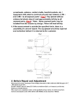
Page 5: ...e the specified limits there is a possibility of a shock hazard The equipment should be repaired and rechecked before it is returned to the customer Fig 1 Fig 2 2 Before Repair and Adjustment Disconne...

Page 6: ...n the indicated rated impedance of the amplifier are used If this occurs follow the procedure outlines below 1 Turn off the power 2 Determine the cause of the problem and correct it 3 Turn on the powe...

Page 7: ...o 4 LD and No 5 GND pins on the flexible board FFC is shorted with a solder build up to prevent damage to the laser diode To connect to the PC board be sure to open by removing the solder build up and...

Page 8: ...to remove the solder from the short point before making connections 6 Precaution of Laser Diode CAUTION This unit utilizes a class 1 laser Invisible laser radiation is emitted from the optical pickup...

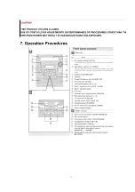
Page 9: ...CAUTION THIS PRODUCT UTILIZES A LASER USE OF CONTROLS OR ADJUSTMENTS OR PERFORMANCE OF PROCEDURES OTHER THAN THOSE SPECIFIED HEREIN MAY RESULT IN HAZARDOUS RADIATION EXPOSURE 7 Operation Procedures 9...

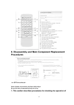
Page 10: ...d Main Component Replacement Procedures ATTENTION SERVICER Some chassis components may have sharp edges Be careful when disassembling and servicing 1 This section describes procedures for checking the...

Page 11: ...C B 1 Checking of the Main Panel Transformer Deck P C B 2 Checking of Power P C B Main Component Replacement Procedures 1 Replacement of the Traverse Deck 2 Replacement of the Power Amplifier IC Disa...

Page 12: ...Step 2 Remove the Top Cabinet Step 3 Push the lever in the direction of the arrow 12...

Page 13: ...Step 4 Pull out the CD tray as shown and remove the CD lid Push back the CD tray after the CD lid has been removed 13...

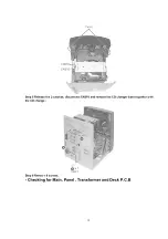
Page 14: ...Step 5 Release the 2 catches disconnect CN310 and remove the CD changer base together with the CD changer Step 6 Remove 8 screws Checking for Main Panel Transformer and Deck P C B 14...

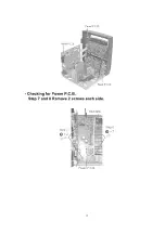
Page 15: ...Checking for Power P C B Step 7 and 8 Remove 2 screws each side 15...

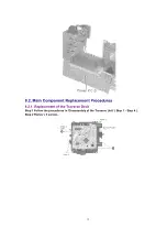
Page 16: ...8 2 Main Component Replacement Procedures 8 2 1 Replacement of the Traverse Deck Step 1 Follow the procedures in Disassembly of the Traverse Unit Step 1 Step 4 Step 2 Remove 3 screws 16...

Page 17: ...3 bosses with a flat screwdriver and pull out the 3 pins Then remove the Traverse Deck Step 5 Remove the flexible cable CN701 Removal of the flexible cable Push the top of the connector in the directi...

Page 18: ...he traverse deck assembly Step 3 Remove 3 screws Note Before installing the CD servo P C B move the optical pickup towards the outer edge from the marking black triangle Otherwise the reset detect swi...

Page 19: ...Step 2 Remove the wires at CN302 CN303 and CN304 and pull out the Main PCB Step 3 Remove the 2 screws fixed to the Power Amplifier IC 19...

Page 20: ...mponent 8 3 Disassembly and assembly of the Traverse Unit Step 1 Push the lever from position A to B Step 2 Pull the stopper black in the direction of arrow 1 and push the lever in the direction of ar...

Page 21: ...Unit Step 1 Place the traverse unit as shown Step 2 Press in the lever shaft in the direction of arrow 1 as shown and push the traverse unit into the position in the direction of arrow 2 Step 3 Pull t...

Page 22: ...tep 5 Push the lever to the initial position indicated 8 4 Disassembly and assembly of the Disc Tray Step 1 Remove 3 screws Step 2 With lifting the claw in the direction of arrow 1 draw the clamp SW P...

Page 23: ...gonal wrench into the hole Step 5 Rotate the hexagonal wrench in the direction of arrow clockwise and then open the disc tray fully Step 6 Upset the CD changer unit again Step 7 Release both the claws...

Page 24: ...cing the left guide bar manually because the left guide bar interferes with claw draw the disc tray Installation of the disc tray after replacement Step 1 Slide the drive rack fully in the direction o...

Page 25: ...Step 2 Holding the drive rack not to move install the disc tray Step 3 Align the drive rack with the drive gear 25...

Page 26: ...nd then push the disc tray 9 Self Diagnostic Function 9 1 Self diagnostic display This unit is equipped with a self diagnostic display function which if a problem occurs will display an error code cor...

Page 27: ...ode H01 H02 H03 F01 F02 1 Press TAPE DECK 1 2 to select Deck 2 2 Load a cassette tape with the erasure prevention tab remove from left side only and close the cassette holder 3 Press FAST FORWARD MEMO...

Page 28: ...TUNE MODE is pressed e g H01 H03 F01 etc 10 Press TAPE DECK 1 2 to select Deck 1 11 Repeat step 2 to 9 to test Deck 1 Tape Deck 1 will not check H02 because of no recording function 9 4 CD Mechanism T...

Page 29: ...sette mechanism Faulty contact or short circuit of mechanism mode switch S951 S971 2 REC INH SW detection error H02 Recording not possible Faulty contact or short circuit of REC INH switch S974 S975 3...

Page 30: ...detect switch or Tray 2 detect switch NG Replace 6 Cannot insert CD F28 Tray 1 detect switch NG Check Replace 7 Cannot eject CD F29 Check if disc is stuck Tray 2 detect switch NG Confirm Replace 8 The...

Page 31: ...er CD test mode pressing the numeric key 0 on the remote controller will display the auto adjustment result FLOCK TLOCK and CLVS status shall be shown as below During the above display executing CD PL...

Page 32: ...NORMAL position 2 Insert the test tape QZZCWAT to DECK 2 and playback FWD side the middle portion of it 3 Adjust Motor VR DECK 2 for the output value shown below Adjustment target 2940 3060 Hz NORMAL...

Page 33: ...justment Deck 1 2 1 Set the unit to AUX position 2 Insert the Normal blank tape QZZCRA into DECK 2 and set the unit to REC mode use REC STOP key 3 Adjust L1002 so that the output frequency is within t...

Page 34: ...AL SETTING INDICATOR ELECTRONIC VOLTMETER OSCILLOSCOPE ADJUSTMENT Shown in Fig 1 REMARKS CONNECTIONSFREQUENCY Fashion a loop of several turns of wire and radiate signal into loop of receiver 520 kHz T...

Page 35: ...Tuner Section 13 Illustration of IC s Transistors and Diodes 14 Terminal Function of IC s 14 1 IC701 AN8885SBE1 Servo Amplifier 35...

Page 36: ...citor for HPF amp connection 12 BDO O BDO output H drop out 13 LDON I APC control 14 GND Ground 15 RFDET O NRFDET output L detection 16 PDOWN O Power down input 17 OFTR O OFTR output 18 NC O N C 19 EN...

Page 37: ...MLD I Microprocessor command load signal input 10 SENSE O Sense signal output OFT FESL MAGEND NAJEND POSAD SFG Not used open 11 FLOCK O Focus servo feeding signal output L Feed 12 TLOCK O Tracking ser...

Page 38: ...or drive signal output forced mode output 25 ECS O Spindle motor drive signal output servo error signal output 26 KICK O N C 27 TRD O Tracking drive output 28 FOD O Focus drive output 29 VREF I D A dr...

Page 39: ...6 DRF I DSL bias terminal Not used open 47 DSLF I O DSL loop filter terminal 48 PLLF I O PLL loop filter terminal 49 VCOF I O VCO loop filter terminal 50 AVDD2 I Power supply input for analog circuit...

Page 40: ...ignal output fCLK 7 35 kHz double 14 7 kHz 64 IPFLAG Interpolation flag output H Interpolation 65 FLAG Flag output 66 CLVS Spindle servo phase synchronizing signal output H CLV L rough servo 67 CRC Su...

Page 41: ...Motor Spindle Motor Driver Pin No Mark I O Function 1 RST RESET output terminal 2 NC N C 3 IN2 I Motor Drive 2 input 4 PC2 I Turntable motor drive signal L ON 5 NC N C 6 IN1 I Motor driver 1 input 7...

Page 42: ...C2BBGF000313 System Microprocessor Pin No Mark I O Function 1 DECK2 I Tape mecha condition input Half2 Reci_F Mode Reci_R 2 KEY3 I Key 3 input 3 KEY2 I Key 2 input 4 KEY1 I Key 1 input 5 NC NC 6 CHG_...

Page 43: ...1 26 MBP2 O MPU beat proof output 2 27 MCLK PLLCK O CD command clock output tuner PLL clock output 28 MDATA PLLDA O CD command data output tuner PLL data output 29 RMT I Remote control input 30 BLKCK...

Page 44: ...D 9 O Digital drive output Grid drive output For regional setting function selection use 81 88 REG8 GRID8 REG1 GRID1 O Digital drive output Grid drive output For regional setting function selection us...

Page 45: ...elopment of the new technology Note S600 Power switch S601 Display switch S602 Disc 1 switch S603 Disc 2 switch S604 Disc 3 switch S605 Disc 4 switch S606 Disc 5 switch S607 CD Open Close switch S701...

Page 46: ...22 Stop Demo switch S923 REW switch S924 Deck 1 Eject switch S925 Deck 1 2 switch S926 Rec Stop switch S928 Preset EQ Subwoofer switch S951 Mode switch S952 Half switch S953 CR02 switch S971 Mode swit...

Page 47: ...by mark have special characteristics important for safety Furthermore special parts which have purposes of fire retardant resistors high quality sound capacitors low noise resistors etc are used When...

Page 48: ...17 Printed Circuit Board Note Circuit board diagrams may be modified at any time with the development of new technology 18 Wiring Connection Diagram 19 Troubleshooting Guide 48...

Page 49: ...20 Parts Location and Replacement Parts List Notes 49...

Page 50: ...ads Resistance values are in ohms unless specified otherwise 1K 1 000 OHM The marking RTL indicates that the Retention Time is limited for this items After the discontinuation of this assembly in prod...

Page 51: ...20 1 Deck Mechanism RAA4501 1S 20 1 1 Deck Mechanism Parts Location 51...

Page 52: ...20 1 2 Deck Mechanism Parts List 52...

Page 53: ...ING LEVER M 119 RML0374 EJECT LEVER M 120 RMM0131 BRAKE ROD M 121 RMM0133 EJECT ROD M 122 RMQ0519 REEL HUB M 123 RMS0398 MOVING CORE M 124 RSJ0003 PLUNGER ASS Y M 125 RMC0061 PACK SPRING M 126 RXF0049...

Page 54: ...54...

Page 55: ...20 2 2 CD Loading Mechanism Parts List 55...

Page 56: ...0257 TRAY LOCK LEVER SPRI M 323 RML0520 TRAY LOCK M 324 RMM0202 SLIDE PLATE 2 M 325 XTB3 10J SCREW M 326 RMR0334 FIXED PLATE M 327 RMR0624 W2 CLAMPER M 328 RMB0561 ASSIST LEVER SPRING M 329 RMR1121 K...

Page 57: ...339 TRAVERSE MOTOR ASSY M 358 7 RXQ0304 1 NUT PLATE ASSY M 358 8 XQN17 CG5 NUT PLATE ASSY SCREW M 358 9 XQS2 A3FZ SPINDLE MOTOR SCREW M 358 10 XQS17 A35FZ TRAVERSE MOTOR SCREW M 359 RME0142 FLOATING S...

Page 58: ...58...

Page 59: ...20 3 2 Cabinet Parts List 59...

Page 60: ...L M 22 RKFX0092 1K CASS LID R M 23 RKFX0093 K CASS HOLDER L M 24 RKFX0094 K CASS HOLDER R M 25 RKMX0066 K TOP CABINET BENT M 26 RKWX0163 H CASS WINDOW L M 27 RKWX0164 H CASS WINDOW R M 28 RKWX0165 H R...

Page 61: ...IC IF MPX M IC102 LC72131MDTRM IC PLL M IC300 C1BB00000654 IC ASP M IC302 C0AABB000117 IC OP AMP HP AMP M IC500 RSN35H1A P IC POWER M IC600 C2BBGF000313 IC MICROPROCESSOR M IC701 AN8885SBE1 IC SERVO A...

Page 62: ...Q512 2SD2144STA TRANSISTOR M Q513 KTA1267GRTA TRANSISTOR M Q600 KRC103MTA TRANSISTOR M Q603 KTC3199GRTA TRANSISTOR M Q604 KTC3199GRTA TRANSISTOR M Q605 KRC102MTA TRANSISTOR M Q608 KTC3199GRTA TRANSIS...

Page 63: ...D317 UDZSTE177R5B DIODE M D402 MA728TX DIODE M D404 DA204KT146 DIODE M D405 MA728TX DIODE M D500 MTZJ15CTA DIODE M D503 MTZJ10BTA DIODE M D504 RVD1SS133TA DIODE M D505 RVD1SS133TA DIODE M D506 RVD1SS1...

Page 64: ...2 EVQ21405R SW DISC 1 M S603 EVQ21405R SW DISC 2 M S604 EVQ21405R SW DISC 3 M S605 EVQ21405R SW DISC 4 M S606 EVQ21405R SW DISC 5 M S607 EVQ21405R SW CD OPEN CLOSE M S701 RSH1A043 U SW REST M S910 EVQ...

Page 65: ...01 RJS2A8616 16P FPC CONNECTOR M CN702 RJS1A6719 1Q 19P FFC CONNECTOR M CN900 RJT066H08D 8 PIN B B CONNECTOR M CN951 RJP13G4YA 13P CONNECTOR M CN952 RJP7G18ZA 7P CONNECTOR M CN1001 52151 0810 8P WIRE...

Page 66: ...F202 RLFFETWND01M FM CF M RELAY RL950 RSY0040M 0 PRIMARY RELAY M OSCILLATORS X102 RLFDFT22DD DISCRIMINATOR M X103 RSXC7M20S05T CRYSTAL OSCILLATOR M X600 RSXD32K7S02 CRYSTAL OSCILLATOR M X601 RSXZ4M19B...

Page 67: ...H601 RMR0317 8P CABLE HOLDER M 67...

Page 68: ...WIR M RESISTORS R1 ERDS2TJ102T 1K 1 4W M R1 ERDS2TJ104T 100K 1 4W M R2 ERDS2TJ104T 100K 1 4W M R3 ERDS2TJ221T 220 1 4W M R4 ERDS2TJ104T 100K 1 4W M R5 ERDS2TJ564T 560K 1 4W M R6 ERDS2TJ391T 390 1 4W...

Page 69: ...R116 ERJ3GEYJ102V 1K 1 16W M 69...

Page 70: ...2 ERJ3GEYJ682V 6 8K 1 16W M R143 ERJ3GEYJ223V 22K 1 16W M R144 ERJ3GEYJ121V 120 1 16W M R145 ERJ3GEYJ104V 100K 1 16W M R146 ERJ3GEYJ104V 100K 1 16W M R151 ERJ3GEYJ820V 82 1 16W M R152 ERJ3GEY0R00V 0 1...

Page 71: ...07 ERJ3GEYJ473V 47K 1 16W M R308 ERJ3GEYJ473V 47K 1 16W M R309 ERJ3GEYJ223V 22K 1 16W M R310 ERJ3GEYJ123V 12K 1 16W M R311 ERJ3GEYJ103V 10K 1 16W M R312 ERJ3GEYJ221V 220 1 16W M R313 ERJ3GEYJ223V 22K...

Page 72: ...J473V 47K 1 16W M R407 ERJ3GEYJ820V 82 1 16W M R408 ERJ3GEYJ562V 5 6K 1 16W M R409 ERJ3GEYJ104V 100K 1 16W M R410 ERJ3GEYJ822V 8 2K 1 16W M R411 ERJ3GEYJ823V 82K 1 16W M R412 ERJ3GEYJ334V 330K 1 16W M...

Page 73: ...S2TJ332T 3 3K 1 4W M R514 ERDS2TJ334T 330K 1 4W M R515 ERDS2TJ563T 56K 1 4W M R516 ERDS2TJ102T 1K 1 4W M R517 ERDS2TJ102T 1K 1 4W M R521 ERDS2TJ563T 56K 1 4W M R531 ERDS2TJ123T 12K 1 4W M R532 ERDS2TJ...

Page 74: ...1 4W M R617 ERDS2TJ104T 100K 1 4W M R618 ERDS2TJ104T 100K 1 4W M R619 ERDS2TJ104T 100K 1 4W M R620 ERDS2TJ104T 100K 1 4W M R621 ERDS2TJ104T 100K 1 4W M R622 ERDS2TJ104T 100K 1 4W M R623 ERDS2TJ104T 1...

Page 75: ...2V 1K 1 16W M R705 ERJ3GEYJ154V 150K 1 16W M R706 ERJ3GEYJ102V 1K 1 16W M R707 ERJ3GEYJ393V 39K 1 16W M R708 ERJ3GEYJ223V 22K 1 16W M R709 ERJ3GEYJ473V 47K 1 16W M R711 ERJ3GEYJ823V 82K 1 16W M R712 E...

Page 76: ...61 ERDS2TJ332T 3 3K 1 4W M R962 ERDS2TJ2R2T 2 2 1 4W M R964 ERC12UGK335D 3 3M 1 2W M R972 ERDS2TJ821T 820 1 4W M R973 ERDS2TJ393T 39K 1 4W M R1001 ERJ3GEYJ1R0V 1 1 16W M R1003 ERJ3GEYJ103V 10K 1 16W M...

Page 77: ...R1060 ERJ3GEYJ391V 390 1 16W M R1061 ERJ3GEYJ2R7V 2 7 1 16W M R1062 ERJ3GEYJ2R7V 2 7 1 16W M R1063 ERJ3GEYJ102V 1K 1 16W M R1064 ERJ3GEYJ102V 1K 1 16W M R1065 ERJ3GEYJ102V 1K 1 16W M R1066 ERJ3GEYJ10...

Page 78: ...V1H080DCV 8P 50V M C109 ECUV1H102KBV 1000P 50V M C110 ECUV1E103KBV 0 01 25V M C111 ECEA1HKA4R7B 4 7 50V M C112 ECUV1E103KBV 0 01 25V M C113 ECUV1H102KBV 1000P 50V M C114 ECEA1HKA3R3B 3 3 50V M C115 EC...

Page 79: ...M C222 ECEA1CKA100B 10 16V M C224 ECUV1C823KBV 0 082 16V M C225 ECUV1H101KCV 100P 50V M C226 ECEA1HKAR68B 0 68 50V M C227 ECUV1H101KCV 100P 50V M C228 ECUV1H470JCV 47P 50V M C229 ECEA1CKA100B 10 16V...

Page 80: ...C416 ECEA1HKAR22B 0 22 50V M C417 ECEA1HKA0R1B 0 1 50V M C418 ECUVNA154KBV 0 15 10V M C419 ECUVNA154KBV 0 15 10V M C420 ECUV1H182KBV 1800P 50V M C421 ECEA1HKA2R2B 2 2 50V M C422 ECEA1CKA100B 10 16V M...

Page 81: ...M102B 1000P 10V M C605 ECBT1H102KB5 1000P 50V M C606 ECBT1H561KB5 560P 50V M C607 ECBT1H561KB5 560P 50V M C608 ECBT1H561KB5 560P 50V M C609 ECBT1H561KB5 560P 50V M C610 ECBT1H561KB5 560P 50V M C611 EC...

Page 82: ...027 25V M C710 ECUV1H121KCV 120P 50V M C711 ECUV1C104ZFV 0 1 16V M C712 ECUV1C104ZFV 0 1 16V M C713 ECUV1C104KBV 0 1 16V M C714 ECEA0JKA101I 100 6 3V M C715 ECUV1H272KBV 2700P 50V M C716 ECUV1H821KBN...

Page 83: ...472JZT 4700P 100V M C1008 ECEA1HKA010B 1 50V M C1009 ECEA1CKA470B 47 16V M C1010 ECA1EM101B 100 25V M C1011 ECQV1H473JL3 0 047 50V M C1012 ECUV1H102KBV 1000P 50V M C1013 ECUV1H102KBV 1000P 50V M C1014...

Page 84: ...C1041 ECEA1CKA100B 10 16V M 84...

Page 85: ...W M RJ704 ERJ6GEY0R00V 0 1 10W M RJ710 ERJ6GEY0R00V 0 1 10W M RJ712 ERJ6GEY0R00V 0 1 10W M RJ713 ERJ6GEY0R00V 0 1 10W M RJ714 ERJ6GEY0R00V 0 1 10W M RJ721 ERJ3GEY0R00V 0 1 16W M RJ722 ERJ3GEY0R00V 0 1...

Page 86: ...P P1 RPGX0919 PACKING CASE M PC P2 RPNX0141 POLYFOAM M P3 RPFX0007 MIRAMAT BAG M ACCESSORIES A1 N2QAGB000016 REMOTE CONTROL M A1 1 BBN11M202A R C BATTERY COVER M A2 RJA0065 1D AC CORD M A3 RQT6351 P O...

Page 87: ...Printed in Singapore P020100001 D K J N L PRT 87...

Page 88: ...430 C230 C231 C431 R231 R431 R232 R432 Q203 R233 Q403 R433 J315 R337 9 15 C401 C201 R401 R402 C402 R202 R201 C202 C333 J285 7 R346 339 J234 J231 R436 R435 R437 R434 C433 C233 R234 R235 R236 R237 Q407...

Page 89: ...M DECK2 P C B REPX0108F FWD CS971 J2 R972 MODE HALF D971 R973 J3 IC971 Z971 J1 CR02 S974 PL PL 1 2 3 4 1 2 3 4 5 6 7 8 9 7 6 5 4 3 2 1 SOLENOID REV S973 S972 S971 S975 CS951 R952 MODE HALF D951 R953 I...

Page 90: ...2 C651 J669 R635 R636 R659 R660 R631 J685 J649 C653 R630 D613 D614 R678 R679 R680 R681 R682 J606 J605 R633 J607 J602 J601 J636 J603 C670 J628 J915 J929 J674 R675 J676 J675 J921 J689 C671 J922 C672 L60...

Page 91: ...2 C658 R673 R683 C657 Q605 C643 Q600 C644 C645 D617 R629 R628 J650 J618 J690 J652 R676 R677 J625 J629 J620 J619 J642 R609 J901 J626 J648 Q608 DISPLAY 6 5 J641 J640 J639 R655 R658 J638 J637 R657 R652 R...

Page 92: ...51 D950 Q953 R961 Q950 C954 C953 R952 R951 D952 R950 D953 R953 R954 D954 CN951 C964 R549 R550 C524 R556 C538 J501 J502 J503 R584 J504 J505 J506 J507 J508 J509 R962 J515 J513 J520 J523 J524 J517 J529 J...

Page 93: ...C743 TJ701 C702 IC702 J707 J708 C745 R744 TP26 TP24 Q701 C736 C738 R741 C722 C721 R711 C724 C718 R709 R712 R742 J721 C723 X701 C728 IC701 J722 J709 J728 J710 J701 R749 C751 C750 J712 C753 R750 J702 J7...

Page 94: ...913 S923 RE S912 TUNER BAND D903 S914 TAPE PLAY S911 CD PLAY S910 STO S922 F S921 DECK2_OP S920 D902 CP900 R914 R915 R916 R917 R918 R919 R920 R910 R911 R912 R913 R922 R925 R924 8 7 6 5 4 3 2 1 DEMO SS...

Page 95: ...0 13 12 11 10 9 8 7 6 5 4 3 2 1 2 1 3 4 1 2 5 4 3 CAUTION RISK OF ELECTRIC SHOCK AC VOLTAGE LINE PLEASE DO NOT TOUCH THIS P C B RISK OF FIRE REPLACE FUSE AS MARKED 1 2 3 4 5 6 7 8 PRIMARY SECONDAR X X...

Page 96: ...5 390 R715 1K R724 18K R735 100 C735 0 1 C734 10V220 R736 100 F SCHEMATIC DIAGRAM 1 CD SERVO CIRCUIT OPTICAL PICKUP CIRCUIT B SIGNAL LINE M M IC703 VCC NC NC RSTIN IN3 IN4 VREF NC RST GND GND PVCC2 PG...

Page 97: ...1 6V 0V 1V 0V 1 6V 0V 0V 0V 1 5V 0V 0V 0V SCHEMATIC DIAGRAM 2 CD SERVO CIRCUIT B SIGNAL LINE CD SIGNAL LINE DVSS1 DVDD1 BCLK LRCK SRDATA TX MCLK MDATA MLD SENSE FLOCK TLOCK BLKCK SQCK SUBQ DMUTE STAT...

Page 98: ...C131 150P C137 3300P C118 0 01 C117 0 01 C142 50V1 R142 6 8K C141 50V1 R141 6 8K R126 1K R125 470 R129 27K R127 470 C124 100P R132 10K C148 0 01 R124 33 X102 RLFDFT22DD C122 50V1 R122 2 7K C121 50V0 4...

Page 99: ...2 KTA12710YTA CD MOTOR SUPPLY SWITCH Q302 IC300 C1BB00000654 AUDIO SOUND PROCESSOR 50V2 2 C211 50V2 2 C212 50V4 7 R386 0 R219 5 6K R220 2 2K C221 50V2 2 R446 0 R419 5 6K R420 2 2K C421 50V2 2 C309 10V...

Page 100: ...R249 470 Q207 Q407 KTD1304TA HEADPHONE MUTING SWITCH R337 47K Q307 Q307 KRA102STA AUDIO MUTING CONTROL SWITCH C310 50V4 7 R339 33K R318 100 R319 100 R320 100 C323 1000P C321 1000P R321 100K R322 100K...

Page 101: ...047 C234 0 047 C434 0 047 MAIN CIRCUIT SCHEMATIC DIAGRAM 6 8 69V 8 64V 1 42V 1 39V 2 06V 2 04V 8 69V 8 75V 1 37V 1 38V 2V 2 02V JK310 FULL RANGE LO_L LO_R OUT_L OUT_R GND_L GND_R GND_R GND_R GND_L GN...

Page 102: ...MO S921 FF S920 DECK2 OPEN R917 1 8K R916 1 2K R915 1K R914 1K D903 SLR325YCT31 D902 SLR325YCT31 R922 270 S600 POWER S601 DISPLAY S602 DISC 1 S603 DISC 2 S604 DISC 3 S605 DISC 4 S606 DISC 5 S607 CD OP...

Page 103: ...2V 32 8V 24 5V 32 8V 26V 0 02V 37 3V 37 7V 28V 32 8V 34V 37 7V 23 2V 27 5V 28 1V 32 8V 27 4V 37 7V 23 2V 28 7V 28 1V 37 7V 23V 32 8V 27 6V 37 6V 29V 32 9V 30 8V 32 9V 27V 16 96V 27 6V 22 9V 21V 22 3V...

Page 104: ...AD1 CHG_AD2 SW1 CHG_CCW CHG_CW CHG_HALF CHG_PLGR SUBQ STATUS CDRST RESTSW PLLCE D GND PCONT SYS6V FL2 FL1 VP D GND SYNC D616 MTZJ5R6BTA R607 22K C639 50V3 3 C642 100P C643 100P R609 100K C644 50V1 R67...

Page 105: ...10K C1026 6 3V47 C1016 2200P C1017 2200P C1013 1000P C1011 0 047 C1018 0 01 R1013 4 7K R1012 4 7K C1014 1000P C1022 1000P C1021 470P C1023 1000P C1027 1000P C1031 10V100 R1016 47 C1033 0 018 R1019 3...

Page 106: ...5 2 2K R1079 4 7K R1066 1K R1065 1K R1061 2 7 R1062 2 7 R1063 1K R1064 1K R1089 22K R1088 22K R1060 390 C1055 50V0 1 R1059 10K R1058 2 7K R1057 2 2K R1056 220 C1054 50V3 3 R1091 2 2K R1094 1K R1085 47...

Page 107: ...TCH C522 0 01 R552 3 3K Q513 R547 27 C528 50V2200P C529 50V2200P VCC IC500 RSN314H41A P HIC IC500 POWER CIRCUIT SCHEMATIC DIAGRAM 12 34 9V 35V 13 96V 13 97V 14 56V 14 57V 38V 38V 12 62V 12 6V 13 2V 13...

Page 108: ...AGE REGULATOR VP C961 100V10 C956 0 01 R960 150 R959 4 7K R958 4 7 C957 63V100 D956 RL1N4003N02 D955 1D3E Q953 Q953 2SD2144STA PCONT SWITCH AC GND 13 12 11 10 2 4 6 8 9 7 5 3 1 H950 W950 FP951 1000 R9...

Page 109: ...ICAL PICKUP CS1001 10 1 H1001 W1001 CN1001 1 8 CP1002 1 9 1 2 3 4 5 1 9 CP1001 CS1002 1 2 3 4 5 X X 7 1 1 13 SOLDER SIDE H POWER P C B CN500 CN501 CN952 CN951 12 1 12 1 D TACT SWITCH P C B C PANEL P C...

Page 110: ...102STA KTC3875GRTA KTD1304TA 2SA1037AKSTX 2SC2412KT96R KTC3199GRTA RVTDTC143EST 2SC2786MTA 2SC2787FL1TA 2SD2144STA 1D3E RL1N4003N02 MTZJ4R7BTA MTZJ5R6BTA MTZJ6R8BTA MTZJ10BTA MTZJ15CTA MTZJ16BTA MTZJ3...

Page 111: ...R MASH LOGIC RST BLKCK SQCK SUBQ TLOCK 14 18 13 12 15 MCLK MDATA MLD 8 7 9 STAT 17 MICROCOMPUTER INTERFACE CRCC CHECK SUB CODE DEMODULATOR 62 CLDCK 56 55 SBCK SUBC 75 OUTR RCH DIGITAL DE EMPHASIS PEAK...

Page 112: ...23 22 ALC BUFFER 6 Z120 RF AMP 5 1 OSC MIXER 8 FM Q101 IF AMP 7 CF201 CF202 13 16 15 14 DECODER STEREO SWITCH AM DET AM IF TUNING DRIVE AM FM IF BUFFER COMP FF FF REG VCO AM MIX AM RM AMP AGC 21 20 19...

Page 113: ...G_CCW CHG_CW STATUS 35 9 34 INTERFACE SWITCH BLKCK ST DO SUBQ Q303 Q304 STATUS Q305 38 CHG_HLF 36 6 CHG_SW1 CHG_AD2 CHG_AD1 7 39 SW5 SW4 CHG_PGR CHG_SW2 37 Q301 SW3 SW1 SW2 Q302 6 IN2 5 IN1 RM1 1 4 7...

Page 114: ...022 9 11 MUTING Q1014 Q1015 NOR CrO HI LO LOGIC LOGIC REC PB RIPPLE REJECTION LOGIC L H ALC 13 14 16 10 18 7 20 5 BUFFER AMP Q1012 Q1013 19 20 X600 XCOUT XCIN FL DISPLAY FL600 81 88 REG8 GRID8 52 78 R...

Page 115: ...17 26 VOL IN1 2 18 25 IC600 C2BBGF000313 MICROPROCESSOR B IC302 C0AABB000117 20 VCC VOLTAGE REGULATOR Q320 D311 HP_L R HEADPHONE MUTING SWITCH Q407 Q207 MUTEH 44 HP_L R CD 42 MUTEH CD 46 SSEQ_LED 18 Q...

Page 116: ...D950 D951 D953 Q950 VOLTAGE REGULATOR RL950 JK950 AC INLET B B FP950 D965 D968 B B D955 D956 D957 FP951 D618 VOLTAGE STABILISER B BACK UP TRANSFORMER Q500 VOLTAGE SUPPLY SWITCH Q501 CURRENT STABILISER...

Page 117: ...578A N CD DETECT P C B REP2578A N SPINDLE POSITION P C B REP2578A N TUNER PACK P C B REP1999B 1 IC1 J3 J1 SW3 R1 D2 Q1 SW1 SW2 W2 W1 CN1 C2 J4 C1 J2 C E B 1 2 3 4 5 6 7 8 9 10 1 2 3 2 3 4 5 6 7 8 9 10...

Page 118: ...93 R1094 R1091 Q1020 R1095 R1092 Q1021 R1096 C1054 C1064 J1028 J1016 J1019 J1021 J1022 J1029 J1034 J1039 J1040 J1043 J1073 J1051 J1052 J1053 J1056 J1057 J1061 J1062 J1067 J1069 J1070 J1074 J1082 J1083...

Page 119: ...C441 R470 R471 R248 C242 R347 CN300 R309 R310 R307 R308 R311 R315 R313 R314 Q301 Q302 R312 C320 J250 R316 R317 Q303 Q304 Q305 R330 C326 R331 C325 R332 C324 R335 R333 R329 R336 R328 R344 C321 C323 C322...

Reviews: