background image

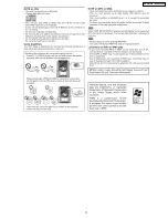
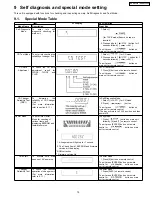
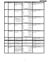
With reference to page 15 of the operating instruction manual.

Note:

* represent tray number (from 1 ~ 5)

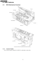
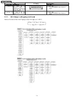
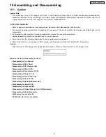
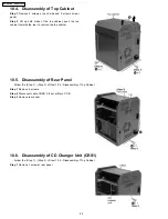
8.1.4. New CD Mechanism (CRS1)

Note:

This service manual does not contain the following information for the mention CD Mechanism drive:


·


Schematic Diagram, Block Diagram and P.C.B. layout of CD Loading P.C.B.


·


Part List for individual parts of the mechanism.


·


Exploded View and Parts List for individual parts of the CD Mechanism drive.

Please refer to the original service manual (Order No. MD0509368C0) for the CD Mechanism Drive CRS1.
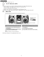
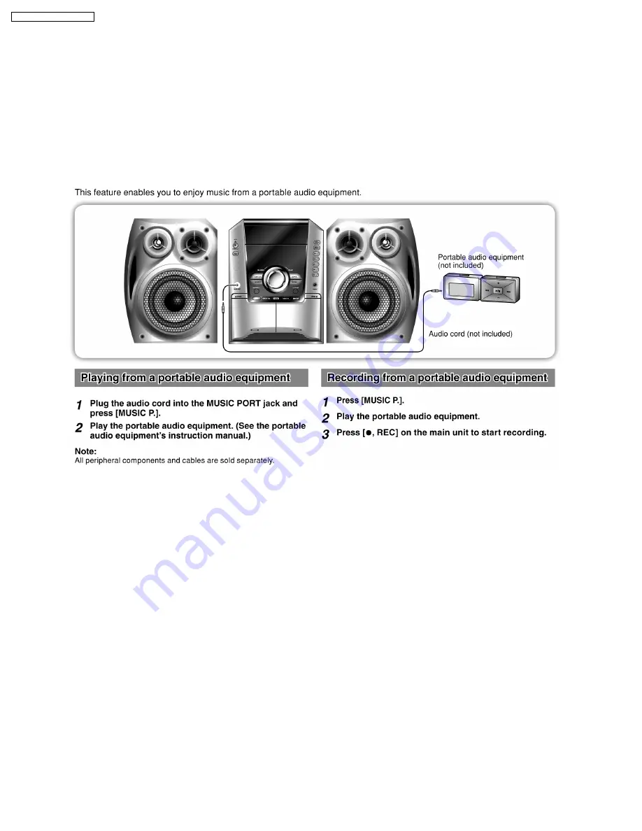
8.2. Music Port

14

SA-AK340P / SA-AK340PC

Summary of Contents for SA-AK340P

Page 1: ...f law SA AK340P SA AK340PC Colour S Silver Type S N 26dB 2 2 µV Antenna terminal s 75 Ω unbalanced Amplitude Modulation AM Frequency range 520 to 1710 kHz 10 kHz step Sensitivity S N 20dB at 1000 kHz 560 µV m Music Port input jack Terminal Stereo 3 5 mm 1 8 jack Sensitivity 100 mV 4 7 kΩ Phone jack Terminal Stereo 3 5 mm 1 8 jack n CASSETTE DECK SECTION Track system 4 track 2 channel Heads Record ...

Page 2: ...Hz Power consumption 125 W Power consumption in standby mode 0 28 W Dimensions W x H x D 250 x 330 x 343 mm 9 27 32 x 13 x 13 1 2 Mass 6 6 kg 14 6 lb Operating temperature range 5 to 35 C 41 to 95 F Operating humidity range 5 to 90 RH no condensation n SYSTEM SC AK340 P Music center SA AK340 P Speaker SB AK340 P SC AK340 PC Music center SA AK340 PC Speaker SB AK340 P Notes 1 Specifications are sub...

Page 3: ...uit G Deck Mechanism Circuit 71 19 Printed Circuit Board 73 19 1 A CD Servo P C B 74 19 2 B Main P C B 75 19 3 C Panel P C B 76 19 4 D Transformer P C B 77 19 5 E Power P C B 78 19 6 F Deck P C B G Deck Mechanism P C B 79 20 Terminal Function of IC s 81 20 1 IC7001 MN6627954MA Servo Processor Digital Signal Processor Digital filter and D A Converter 81 20 2 IC7003 BA5948FPE2 IC 4CH Drive 82 20 3 I...

Page 4: ...ance value between the jumpered AC plug and each exposed metallic cabinet part on the equipment such as screwheads connectors control shafts etc When the exposed metallic part has a return path to the chassis the reading should be between 1MΩ and 5 2MΩ When the exposed metal does not have a return path to the chassis the reading must be Fig 1 1 1 2 Leakage Current Hot Check See Figure 1 1 Plug the...

Page 5: ...rior to applying power to the unit under test 2 After removing an electrical assembly equiped with ES devices place the assembly on a conductive surface such as aluminium foil to prevent electrostatic charge build up or exposure of the assembly 3 Use only a grounded tip soldering iron to solder or unsolder ES devices 4 Use only an anti static solder remover device Some solder removal devices not c...

Page 6: ...riable resistor on the optical pickup lens 4 Do not disassemble the optical optical pickup unit 5 If the optical pickup is replaced use the manufacturer s specified replacement pickup only 6 Use of control or adjustments or performance of procedures other than those specified herein may result in hazardous radiation exposure CAUTION THIS PRODUCT UTILIZES A LASER USE OF CONTROLS OR ADJUSTMENTS OR P...

Page 7: ...elting point is 50 70 F 30 40 C higher Please use a high temperature soldering iron In case of soldering iron with temperature control please set it to 700 20 F 370 10 C Pb free solder will tend to splash when heated too high about 1100 F 600 C When soldering or unsoldering please completely remove all of the solder on the pins or solder area and be sure to heat the soldering points with the Pb fr...

Page 8: ... pin finish the job in as short time as possible 4 Do not turn the variable resistor for laser power adjustment It is pre adjusted during production time Grounding for electrostatic breakdown prevention 1 Human body grounding Use the anti static wrist strap to discharge the static electricity from your body 2 Work table grounding Put a conductive material sheet or steel sheet on the area where the...

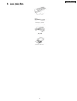
Page 9: ...6 Accessories Remote Control FM Indoor Antenna AC Cord AM Loop Antenna 9 SA AK340P SA AK340PC ...

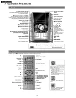
Page 10: ...7 Operation Procedures 10 SA AK340P SA AK340PC ...

Page 11: ...11 SA AK340P SA AK340PC ...

Page 12: ...8 New Features 8 1 CRS1 Mechanism Overview 8 1 1 General Feature This is a five disc changer mechanism for CD DVD The outline figure is shown below 12 SA AK340P SA AK340PC ...

Page 13: ...men 8 1 3 Mechanism Operation This mechanism has the following state 1 Driving of a tray to open close 2 Up down operation of a traverse performs a state changes of tray By using the plunger to lift release of a switching gear and the cam gear to lift release the function gear the motor can be link to several gear trains to perform various operations The functions that can be perform in this mecha...

Page 14: ...ing information for the mention CD Mechanism drive Schematic Diagram Block Diagram and P C B layout of CD Loading P C B Part List for individual parts of the mechanism Exploded View and Parts List for individual parts of the CD Mechanism drive Please refer to the original service manual Order No MD0509368C0 for the CD Mechanism Drive CRS1 8 2 Music Port 14 SA AK340P SA AK340PC ...

Page 15: ... Changer Unit For more information refer to section 9 1 1 In Self Diagnostic Mode 1 Select for CD mode 2 Press button To exit press button on main unit or remote control The tray will return to PLAY position and then power off Doctor Mode To enter into Doctor Mode for checking of various items and displaying EEPROM and firmware version 1 2 1 All segments will light up for 1 second 2 The Check Sum ...

Page 16: ...D will blink at 0 5 second interval In doctor mode 1 Press PROGRAM button on remote control Tape Eject Test To check on the tape eject function For deck 1 2 In doctor mode 1 Press PROGRAM button on remote control 9 1 1 CD changer unit ageing test mode Below is the process flow chart of ageing for the CD changer unit CRS1 16 SA AK340P SA AK340PC ...

Page 17: ...refer Section 9 1 provides information on any problems occuring for the unit and its respective components by displaying the error codes These error code such as U H and F are stored in memory and held unless it is cleared 17 SA AK340P SA AK340PC ...

Page 18: ...Low a fail safe time after system command transmission is sent For CD unit For Traverse Press on main unit for next error F61 Power Amp IC output abnormal Upon power on PCONT HIGH DCDET L after checking LSI For power Press on main unit for next error IHMS Cam gear abnormality Cam gear does not rotate to HOME position For CD changer unit CRS1 Press SINGLE CHANGE on main unit for next error ICSL Cam...

Page 19: ...main unit for next error PDRV Cam gear gear assembly abnormal Cam gear does not move from HOME to PLAY drive position For CD changer unit CRS1 Press SINGLE CHANGE on main unit for next error UDU UD base asssembly abnormal UD Base assembly does not move upwards from tray 5 to tray 2 For CD changer unit CRS1 Press SINGLE CHANGE on main unit for next error UDD UD base asssembly abnormal UD Base assem...

Page 20: ...SINGLE CHANGE on main unit for next error CRS1 Error Code display 1 The errors that occured in CRS1 Mechanism can be recalled and displayed in the order of the occurence under self diagnostic Refer to Section 9 1 1 for procedures to enter this mode Only the first 5 errors will be memorized in backup memory The subsequence error shall be ignored and not memorize For system with EEPROM as memory bac...

Page 21: ...acement reverse the respective procedures Special reassembly procedures are described only when required 3 Select items from the following index when checks or replacement are required 4 Refer to the Parts No on the page of Parts Location and Replacement Parts List Section 22 if necessary Caution After replacing of CD Changer Unit ageing test is necessary Please confirm operation for CD Changer Un...

Page 22: ...The following chart is the procedure for disassembling the casing and inside parts for internal inspection when carrying out the servicing To assemble the unit reverse the steps shown in the chart as below 22 SA AK340P SA AK340PC ...

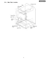
Page 23: ...10 3 Main Parts Location 23 SA AK340P SA AK340PC ...

Page 24: ...emove 5 screws Step 2 Disconnect cable CN2810 Fan at Main P C B Step 3 Remove rear panel Step 1 Remove 1 screw at rear panel 10 4 Disassembly of Top Cabinet 10 5 Disassembly of Rear Panel Follow the Step 1 Step 2 of Item 10 4 Disassembly of Top Cabinet 10 6 Disassembly of CD Changer Unit CRS1 Follow the Step 1 Step 2 of Item 10 4 Disassembly of Top Cabinet 24 SA AK340P SA AK340PC ...

Page 25: ... to remove it Disassembly of Mecha Chassis Step 5 Remove 2 screws Step 6 Remove the Mecha Chassis Note For disassembly assembly of traverse unit please refer to section 10 14 of this service manual Please refer to original Service Manual for the Disassembly and Assembly of the CD Changer Unit CRS1 25 SA AK340P SA AK340PC ...

Page 26: ... CN2809 Step 3 Remove Main P C B Follow the Step 1 Step 2 of Item 10 4 Disassembly of Top Cabinet Follow the Step 1 Step 4 of Item 10 6 Disassembly of CD Changer Unit Follow the Step 1 Step 3 of Item 10 5 Disassembly of Rear Panel 10 8 Disassembly of Transformer P C B Follow the Step 1 Step 2 of Item 10 4 Disassembly of Top Cabinet Follow the Step 1 Step 3 of Item 10 5 Disassembly of Rear Panel Fo...

Page 27: ... screws to Voltage Regulator Step 5 Cut the joints with a metal cutter as shown below Step 6 Desolder the terminals to replace the components Step 7 Fix back the cut portion with a screw as shown 10 9 Disassembly of Power P C B Follow the Step 1 Step 2 of Item 10 4 Disassembly of Top Cabinet Follow the Step 1 Step 4 of Item 10 6 Disassembly of CD Changer Unit Follow the Step 1 Step 3 of Item 10 5 ...

Page 28: ...n each side of bottom chassis to be aligned to front panel s slot Assembly is secured upon hearing clicking sound 10 10 Disassembly of Front Panel Unit Follow the Step 1 Step 2 of Item 10 4 Disassembly of Top Cabinet Follow the Step 1 Step 4 of Item 10 6 Disassembly of CD Changer Unit 10 11 Disassembly for Panel P C B Follow the Step 1 Step 2 of Item 10 4 Disassembly of Top Cabinet Follow the Step...

Page 29: ...p 2 Remove 11 screws Step 3 Release 2 catches Step 4 Remove Panel P C B 10 11 1 Disassembly of Lid Step 1 Lift the spring sideward Step 2 Remove Lid Note Do not misplace the spring 29 SA AK340P SA AK340PC ...

Page 30: ...k mechanism unit refer to Section 10 15 Step 2 Desolder wire at deck motor terminals W1002 Step 3 Remove Deck P C B 10 12 Disassembly of Deck mechanism unit Follow the Step 1 Step 2 of Item 10 4 Disassembly of Top Cabinet Follow the Step 1 Step 4 of Item 10 6 Disassembly of CD Changer Unit Follow the Step 1 Step 4 of Item 10 10 Disassembly of Front Panel Unit 10 13 Disassembly of Deck P C B Follow...

Page 31: ...ep 2 Push the traverse slide plate as arrow shown to release the traverse unit Caution Do not exert strong force on the traverse slide plate Step 3 Remove the traverse unit as arrow shown Assembly of Traverse Unit Step 1 Turn over the unit and install the traverse unit 31 SA AK340P SA AK340PC ...

Page 32: ...Pull out FFC Step 2 Widening the catch push the pin in Step 3 Remove 4 pins 10 15 Disassembly of optical pickup unit CD mechanism Follow the Step 1 Step 2 of Item 10 4 Disassembly of Top Cabinet Follow the Step 1 Step 4 of Item 10 6 Disassembly of CD Changer Unit 32 SA AK340P SA AK340PC ...

Page 33: ...t over Note Insert a short pin into FFC of the optical pickup Step 7 Rotate the traverse deck B to the arrow direction and shift the optical pickup to the furthest backward Step 8 Remove the catch of the drive rack and take out the drive rack Step 9 Place the convex part of an optical pickup to the concave part of a traverse base then take out the optical pickup 33 SA AK340P SA AK340PC ...

Page 34: ...34 SA AK340P SA AK340PC ...

Page 35: ... block Step 4 Remove 3 screws for deck 1 2 Step 5 Remove capstan belt A B 10 16 Disassembly of deck mechanism Follow the Step 1 Step 2 of Item 10 4 Disassembly of Top Cabinet Follow the Step 1 Step 4 of Item 10 6 Disassembly of CD Changer Unit Follow the Step 1 Step 4 of Item 10 10 Disassembly of Front Panel Unit Follow the Step 1 Step 5 of Item 10 12 Disassembly of Deck Mechanism Unit 10 16 1 Dis...

Page 36: ...ss and marking should be positioned horizontally Step 2 Put the winding belt on the pulley temporarily Step 3 Install the flywheel F Step 4 Put the winding belt on the flywheel F Step 5 Install the winding lever and spring while pressing the winding arm in the direction of arrow Step 6 Install the flywheel R 36 SA AK340P SA AK340PC ...

Page 37: ...anism and then tighten screws Step 1 Lift up the lever upward open the cassette deck For DECK1 and DECK2 Step 10 Install 3 screws Step 11 Put the capstan belt B as shown below Step 12 Put the capstan belt A on the motor ass y pulley 10 17 Replacement for cassette lid Follow the Step 1 Step 2 of Item 10 4 Disassembly of Top Cabinet 37 SA AK340P SA AK340PC ...

Page 38: ...e flywheel F in the direction of the arrow to remove it Step 2 Push the lever upward and open the cassette lid Remove the cassette tape Step 2 Push up the cassette lid L R in the direction of arrow For DECK1 and DECK2 10 18 Rectification for tape jam problem Follow the Step 1 Step 2 of Item 10 4 Disassembly of Top Cabinet 38 SA AK340P SA AK340PC ...

Page 39: ... FFC A Deck P C B Main P C B REEX0485 14 Pins B Panel P C B Deck Mechanism P C B REEX0484 10 Pins 12 Service Positions Note For description of the disassembly procedures see the Section 10 12 1 Checking and Repairing of Main P C B 39 SA AK340P SA AK340PC ...

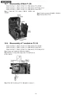
Page 40: ...12 2 Checking and Repairing of Transformer P C B 40 SA AK340P SA AK340PC ...

Page 41: ...12 3 Checking and Repairing of Panel Deck Deck Mechanism P C B 41 SA AK340P SA AK340PC ...

Page 42: ...12 4 Checking and Repairing of Power P C B 42 SA AK340P SA AK340PC ...

Page 43: ... frequency of the DECK 1 FWD are within 60 Hz of the value of the output frequency of DECK 2 FWD Fig 1 13 1 2 Bias Voltage Check 1 Set the unit AUX position 2 Insert the Normal blank tape QZZCRA into DECK 2 and the unit to REC mode use l REC STOP key 3 Measure and make sure that the output is within the standard value Bias voltage for Deck 2 14 4mV Normal Fig 2 Fig 3 13 Measurements and Adjustment...

Page 44: ...requency is maximized at 450kHz in Fig 6 Fig 5 Fig 6 13 2 2 AM RF Adjustment 1 Set up the equipments as shown in Fig 7 2 Select TUNER on selector and set to AM mode 3 Set AM SG to 520kHz 4 Receive 520kHz in the unit 5 Adjust L2601 OSC so that the EVM AC is maximized 6 Set AM SG to 600Hz 7 Receive 600Hz in the unit 8 Adjust L2601 ANT so that the EVM SG is maximized 9 Set AM SG to 520kHz 10 Receive ...

Page 45: ...Fig 7 13 2 3 Adjustment Point Below is the locations of alignment points on the Main Tuner P C B 45 SA AK340P SA AK340PC ...

Page 46: ...escribed herein shall be regarded as reference information when probing defect point because it may differ from an actual measuring value due to difference of Measuring instrument and its measuring condition and product itself 14 1 Main P C B 46 SA AK340P SA AK340PC ...

Page 47: ...14 2 Power P C B and Transformer P C B 47 SA AK340P SA AK340PC ...

Page 48: ...14 3 Waveform Chart 48 SA AK340P SA AK340PC ...

Page 49: ...Ca A Cathode Anode B3AAA0000583 B0ADCC000002 B0BC7R500001 Cathode Ca A Anode B0BC9R000008 A Ca Cathode Anode C1BB00001121 100P C2CBYY000053 100P C0HBB0000057 44P MN6627954MA 100P 1 B0BA01500003 B0BA01900005 A Ca Anode Cathde 1 28 15 14 7 21 22 8 BA5948FPE2 A Ca Cathode Anode MAZ80560ML E C B E C B B1CECC000003 C1BA00000407 1 18 B0EAMM000038 A Ca Anode Cathode B0AACK000004 B0EAKM000122 C0GAG0000007...

Page 50: ...TOR M7301 A CD SERVO P C B M M CN7002 1 2 16 17 PbF SOLDER SIDE SOLDER SIDE B MAIN P C B FM ANT AM ANT JK2601 H TUNER PACK P C B TUNER PACK PbF CN2809 1 12 1 12 CN2808 CN2803 14 2 13 1 CN2951 10 2 9 1 CN2811 1 7 2 8 29 1 30 2 CN2806 CN2805 1 15 2 14 1 2 17 16 CN2801 1 2 To Fan CN2810 FAN MOTOR 2 1 BLACK RED SENSOR Z6481 JK6551 JK6751 VOLUME VR6491 CN6601 30 2 29 1 JK5101 JK5102 E POWER P C B SOLDE...

Page 51: ...RST LPD ARFF PC SPOUT TRVP TRP FOP ARFOUT ARFDC RFOUT RFIN CENV CTRCRS OSCIN VREF RFENV PC SPOUT TRVP TRP FOP LD PD A B C D E F NSRVMONON NTEST2 MDATA ARFIN ARFF BLKCK IREF DSLF PLLF PLLFO TXTCK SBCK PRAMVDD33 PRAMVSS33 D0 D15 A0 A11 BA0 BA1 TXTD DQSY SUBC TXNCLDCK BLKCK FLAG 65 71 20 18 83 92 94 99 1 7 11 15 16 17 NWE NCAS 8 9 63 64 62 NRAS SDRCK LRCK BCLK SRDATA EXT0 EXT2 EXT1 10 100 DVDD2 76 MC...

Page 52: ...1004 Q1003 SWITCHING BEAT PROOF RECH L1002 95 PHOTO_2 IC951 PHOTO INTERRUPTER CNB13030R2AU IC971 PHOTO INTERRU CNB13030R 97 PHOT0_1 6 19 15 12 21 4 22 3 17 8 1 2 24 23 3 5 2 4 Q2980 DECK MOTOR SWITCH M1002 S951 MODE 52 HALF_1 53 MODE_1 S952 HALF Z971 INTERFACE 91 DECK2 S972 HALF S975 RECINH_F S971 MODE DECK 2 R P HEAD LCH Q1017 MOTOR SWITCH M DECK 2 ERASE HEAD DECK 1 P B HEAD LCH MLD MCLK CE MDATA...

Page 53: ... R P HEAD LCH B Q1017 MOTOR SWITCH M DECK 2 ERASE HEAD DECK 1 P B HEAD LCH IC2803 C1BB00001121 AUDIO SOUND PROCESSOR JK2801 AUX S6101 S6108 S6201 S6207 S6302 S6307 Q2317 Q METER CONTROL SWITCH MUTING CONTROL MUTING CONTROL MUTIN CONTR AGC CONTROL SWITCH Q2511 Q2411 Q2311 Q2142 Q2242 DATA 40 CLK 39 26 ASP_DAT 27 ASP_CLK 47 DCDET IN L1 R1 IN L3 R3 IN L2 R2 1 2 3 4 REC L R 53 17 GV OUT L R 54 16 IN_L...

Page 54: ...5 Q5952 SYSTEM 6V VOLTAGE REGULATOR JK5950 AC INLET L5950 LINE FILTER D5950 D5953 FP5950 FP5940 SUB TRANSFORMER D5954 D5957 Q5112 Q5114 5 7V VOLTAGE REGULATOR 15V VOLTAGE REGULATOR CURRENT STABLISER LIMITER SWITCH 11V VOLTAGE REGULATOR Q5101 Q5110 Q5111 FP5920 Q5102 Q5108 Q5109 Q2950 Q2952 C1BA00000407 2 CH DIGITAL AMP IC5301 11 13 VSSP1 2 8 16 VDDP1 2 IN1 IN1 2 3 IN2 21 IN1 3 IN2 21 IN2 22 OSC 1 ...

Page 55: ...measured by DC electronic voltmeter high impedance and oscilloscope on the basis of chassis Accordingly there may arise some error in voltage values and waveforms depending upon the internal impedance of the tester or the measuring unit Importance safety notice Components identified by mark have special characteristics important for safety Furthermore special parts which have purposes of fire reta...

Page 56: ...56 SA AK340P SA AK340PC ...

Page 57: ... 056 W7027 0 C7315 0 47 R7323 3 3K R7327 1K R7335 100 C7335 0 1 C7334 10V220 R7336 10 F C7670 0 1 C7626 0 1 R7315 3 3K R7325 330 IC7002 BA5948FPE2 4 CH DRIVE VCC NC NC NC IN3 IN4 VREF NC GND GND PVCC2 PGND2 D4 D4 D3 D3 PGND1 PVCC1 NC D2 D2 D1 D1 IN1 NC NC PC2 PC1 IN2 NC 3 4 5 6 24 25 26 27 28 8 1 2 23 21 9 20 10 19 1 11 18 2 13 17 16 15 22 7 14 R7339 1K A 12 11 10 2 4 6 8 9 7 5 3 1 13 14 15 16 CN7...

Page 58: ...SA AK340P SA AK340PC 58 ...

Page 59: ...V10 R2621 22K R2602 4 7K C2639 50V4 7 C2618 0 01 C2617 0 01 C2642 50V1 R2642 6 8K C2641 50V1 R2641 6 8K R2626 1K R2625 470 R2629 27K R2627 470 C2624 100P R2632 10K C2648 0 01 R2624 33 X2602 H3F1065A0002 C2622 50V1 R2622 2 7K C2621 50V0 47 R2631 120 R2644 120 R2633 W2919 0 1K C2629 6 3V100 C2649 0 1 C2623 50V1 R2645 100K C2643 6800P C2644 6800P R2646 100K TO MAIN CIRCUIT 2A ON SCHEMATIC DIAGRAM 3 1...

Page 60: ...SA AK340P SA AK340PC 60 ...

Page 61: ...2 REC 59 MTR 58 DECK_H R2675 Q2978 B1GDCFJJ0047 REC ON OFF CONTROL SWITCH Q2980 B1GDCFJJ0047 SUPPLY CONTROL SWITCH DECK MOTOR Q2501 B1ABCF000176 LEVEL METER CONTROL SWITCH R2248 6 8K 2 3 4 7 6 5 R2702 1K Q2341 Q2441 B1ABCF000176 HEADPHONE MUTING R2345 10K R2445 10K R2357 100K R2457 100K C2344 0 47 C2444 0 47 R2447 1 R2446 3 3K R2346 3 3K R2347 1 R R R2442 0 R2444 0 R R R2342 0 R2344 0 Q2511 B1GDCF...

Page 62: ...2334 0 R2326 0 R2430 0 R2328 15K R2317 18K R2356 180K R2456 180K R2417 18K C2343 0 47 C2443 0 47 R2416 2 2K C2331 4700P C2321 1 R2318 100K W2508 0 R2418 100K R2333 15K R2323 39K R2423 39K W2512 0 R2435 1K R2429 3 3K C2431 4700P R2421 0 C2421 1 1 2 3 4 5 6 7 8 9 10 11 12 HIGH_L IN 15V MUTE D AMP T GND F_HOP CN2809 A_GND LOW_R IN FAN LOW_L IN ASP_GND HIGH_R IN C2333 1 C2323 0 015 R2434 0 Q2341 Q2441...

Page 63: ...004 R2803 10K R2861 100 R2955 270K R2866 47K R2865 47K R2854 47K R2857 47K R2856 47K R2855 47K R2863 47K R2950 470K R2965 4 7K R2952 1K SW5V SPEED VREF R2873 22K R2871 22K R2874 4 7K C2871 330P C2874 330P W2532 0 C2872 0 022 1 2 3 4 8 7 6 5 NC VCC EE_CS EE_CLK NC IC2871 GND EE DAT IC2871 C3EBEG000073 E EPROM IC R2936 1K B0EAKM000117 D2936 W2559 0 W2560 0 W2555 0 W2556 0 W2539 0 R2937 10K CN2806 Q2...

Page 64: ... 000053 CESSOR W2557 0 R2846 4 7K R2845 10K R2844 10K R2842 10K W2523 0 R2841 10K R2820 100K R2819 100K R2818 100K R2817 100K R2830 100K R2831 100K R2832 100K R2833 100K W2547 0 W2537 0 W2536 0 W2576 0 W2548 0 W2549 0 R2810 22K R2802 100 C2821 100P R2882 10M W2552 0 R2883 330K C2883 18P R2886 1M R2881 220 C2803 1 C2852 16V100 C2853 0 1 R2851 47K C2940 0 1 R2940 820K D2803 B0ACCK000005 D2801 B0ACCK...

Page 65: ...6 7 8 9 10 11 12 13 14 15 16 17 18 19 20 21 22 23 24 25 26 27 28 29 30 31 32 33 34 35 36 37 38 39 40 41 42 43 44 1 2 3 4 5 6 8 7 9 S6101 POWER S6102 SINGLE DISC CHANGE R6103 2 2K S6103 OPEN CLOSE R6104 1 8K S6104 CD1 CD2 CD3 CD4 CD5 R6105 2 2K S6105 R6106 2 7K S6106 R6107 4 7K S6107 R6108 6 8K R6109 10K R6110 22K S6108 S6302 TAPE S6303 STOP S6304 REC S6305 TUNER BAND S6306 MUSIC P S6308 MULTI DISC...

Page 66: ...SA AK340P SA AK340PC 66 ...

Page 67: ...A6R800008 C5963 50V4 7 R5958 10K R5957 10K C5954 0 01 JK5950 FL2 VP FL1 SYS6V SYS6V PCONT SYNC D_GND TO POWER CIRCUIT H5104 W5104 ON SCHEMATIC DIAGRAM 6 TO PANEL CIRCUIT H6555 W6555 ON SCHEMATIC DIAGRAM 4 Q5951 2SB0621AHA Q5952 Q5952 B1GACFJJ0018 SYNCHRONISATION SWITCH T5951 RTP1H3E002 C5960 D5952 D5950 D5951 D5953 0 1 D5954 D5955 D5956 D5957 C5959 0 01 Z5950 ERZV10V511CS L5950 ELF15N035AN C5961 1...

Page 68: ...SA AK340P SA AK340PC 68 ...

Page 69: ...00001 L5604 G0B9R5K00001 R5405 22 C5432 220P C5430 220P C5418 0 1 C5420 0 1 C5423 0 1 R5407 10 R5408 10 C5406 0 47 C5404 0 47 C5436 1000P R5403 5 6K R5404 5 6K C5405 330P C5401 0 47 R5401 5 6K C5403 0 47 C5437 1000P R5402 5 6K C5402 330P C5422 0 1 2 3 1 4 C5117 35V470P C5118 35V470P HL_L LQ_L C5431 220P C5433 220P R5154 100 Q5154 B1ADCF000063 PCONT SWITCH Q5153 Q5153 B1ABCF000176 MODE SWITCH Q5173...

Page 70: ...210 220P R5209 10 C5208 6 3V680P C5204 100P X5201 H2A415300001 X5202 H2A375300003 Q5202 Q5201 C5701 F_HOP AGND AGND 100 IC5201 C0JBAB000011 LOGIC IC5201 1 14 2 3 4 5 13 12 11 10 6 9 8 7 R5406 22 C5424 0 68 C5427 0 68 L5603 G0B9R5K00001 L5604 G0B9R5K00001 R5405 22 C5432 220P C5430 220P R5407 10 R5408 10 C5406 0 47 C5404 0 47 C5436 1000P R5403 5 6K R5404 5 6K C5405 330P C5401 0 47 R5401 5 6K C5403 0...

Page 71: ... 0 047 C1008 50V1 C1034 50V3 3 R1032 10K R1055 2 2K C1038 220P C1042 16V22 R1031 27K R1035 10K R1030 100 5 11 12 TAPE B INPUT TAPE B INPUT TAPE A INPUT TAPE A INPUT PB AMP NF PB AMP NF PB AMP EQ PB AMP EQ PB AMP OUTPUT PB AMP OUTPUT AB SW T REC IN REC IN REC OUT REC OUT REC PB SW AB SW RIPPLE FILTER OUTPUT GND VCC CRO NOR HI LO ALC T ALC LOW CUT IC1001 SW GND CTRL2 CTRL1 3 C1058 1000P R1100 0 R110...

Page 72: ...SA AK340P SA AK340PC 72 ...

Page 73: ...19 Printed Circuit Board Note Circuit board diagrams may be modified at any time with the development of new technology SA AK340P SA AK340PC 73 ...

Page 74: ...028 C7243 TP4 X C7234 R7254 W7009 W7001 CN7002 W7010 C7235 W7011 TP3 X TP31 X TP1 X R7332 TP39 X TP10 X TP8 X TP7 X TP9 X M7301 TRV MOTOR TP38 X TP11 X TP36 X M7302 SPL MOTOR TP37 X R7335 R7325 R7315 TP2 X S7201 REST SW C7264 R7214 R7220 X7201 C7263 C7166 C7230 C7216 R7212 W7013 C7241 C7217 R7211 C7244 W7012 C7223 C7203 W7014 W7015 C7204 TP51 RF C7161 C7102 C7142 C7107 IC7001 R7331 C7165 C7315 R73...

Page 75: ...C2301 C2172 C2171 R2172 R2173 C2173 C2174 C2175 C2183 C2181 C2431 W2319 C2182 R2182 C2101 C2433 R2434 R2435 W2510 C2333 R2334 R2326 C2325 W2136 W2137 K2302 W2130 W2140 W2141 C2425 C2943 CN2809 W2132 W2131 R2111 R2112 R2104 C2113 R2102 C2124 W2178 W2179 C2224 C2122 C2112 C2114 C2212 C2214 C2222 C2132 C2232 R2183 R2181 C2252 C2152 IC2803 C2401 C2402 R2401 C2275 C2195 C2194 R2195 R2196 R2194 C2193 R2...

Page 76: ...R6204 W6054 W6085 W6059 W6051 W6050 W6048 C6481 W6402 FL6602 R6605 W6044 W6045 W6046 W6047 D6462 VR6491 D6457 C6492 C6491 W6052 R6492 K6104 QR6457 K6051 P K6002 AK340 R6205 S6204 H BASS S6202 DISPLAY DEMO R6206 W6081 W6080 R6491 W6040 R6457 W6049 W6043 W6038 W6503 W6504 W6505 IC6601 R6458 R6604 R6603 R6601 C6604 C6603 C6601 R6493 W6004 W6082 W6003 W6002 W6017 W6014 W6012 R6199 W6032 CN6601 W6018 W...

Page 77: ...61 C5961 C5951 C5962 D5962 R5957 C5963 Q5952 R5958 R5951 Q5951 CN5951 W5923 W5922 W5906 W5904 CN5950 W5920 W5907 W5908 W5902 C5940 W5930 W5901 C5956 D5959 D5958 C5955 D5951 D5953 C5920 W5903 FP5920 7A FP5940 7A W5909 C5958 C5957 D5960 W5905 R5960 Q5953 R5961 D5966 C5954 C5952 R5963 D5964 C5953 Q5950 D5952 D5950 C5950 D5956 D5957 D5955 D5954 C5959 FP5950 4A W5910 C5960 D5965 R5950 SUB TRANSFORMER R...

Page 78: ...5 W5136 W5140 C5415 C5417 W5139 W5141 C5418 C5421 C5420 C5118 C5405 R5418 W5505 R5112 R5113 R5303 C5304 W5123 W5127 W5126 R5152 C5303 C5301 R5301 Q5104 C5105 C5155 R5111 W5131 W5132 W5130 R5302 W5151 J5103 W5148 C5403R5402 C5306 R5304 W5507 C5437 W5150 C5337 W5149 C5401 R5401 R5404 W5506 C5406 C5404 R5403 W5133 L5401 W5156 L5402 R5135 R5136 R5137 D5109 C5113 R5134 W5508 Q5111 Q5114 Q5113 R5147 D51...

Page 79: ...008 Q1003 J1002 C1007 C1002 C1026 J1003 C1011 C1040 C1034 Q1017 C1044 C1043 J1016 J1008 J1009 C1010 J1111 J1011 J1020 J1012 J1013 J1022 J1028 J1038 J1014 J1033 J1023 J1021 J1015 C1046 Q1005 R1007 W1002 CS1002 TO R P HEAD CS1001 TO P B HEAD L1002 IC1004 C1041 CN1001 J1010 J1004 C1030 C1032 C1045 C1033 C1037 C1056 C1031 C1035 C1042 J1064 J1051 L1001 Q1004 J1006 J9999 R1005 R1003 C1021 R1010 R1097 R1...

Page 80: ...SA AK340P SA AK340PC 80 ...

Page 81: ...ARF Feedback Signal I P 51 ARFIN I Audio RF Signal I P 52 DSLF I Loop Filter Terminal For DSL Pin No Mark I O Function 53 IREF I Reference I P 54 PLLF I PLL Loop Filter Terminal Phase Compare 55 PLLF0 O PLL Loop Filter Terminal Speed Compare 56 OUTL O Audio O P LCH 57 AVSS1 I GND 58 AVDD1 I Analog Power Supply Voltage 1 59 OUTR O Audio O P RCH 60 DVSS3 I GND3 Digital Circuit 61 NSRVMONON I Servo M...

Page 82: ...dio Mute 41 EE_CS EFP EPH O EEPROM Chip Select 42 EE_CLK O EEPROM CLOCK Pin No Mark I O Function 15 D3 O Motor Drive 3 reverse action output 16 D3 O Motor Drive 3 forward action output 17 D4 O Motor Drive 4 reverse action output 18 D4 O Motor Drive 4 forward action output 19 PVCC2 Power Supply 2 for Driver 20 PGND2 Ground Connection 2 for Driver 21 24 N C O No Connection 25 VCC I Power Supply term...

Page 83: ...R I UD Sensor for CRS1 91 DECK2 I DECK CONDITION INPUT 2 R_INHF MODE2 HALF2 92 KEY3 I KEY3 INPUT 93 KEY2 I KEY2 INPUT 94 KEY1 I KEY1 INPUT 95 PHOTO_2 I Rotation Detection Signal Deck 2 96 AVSS Analog Power Supply Input Connect to GND 97 PHOTO_1 I Rotation Detection Signal Deck 1 98 VREF Reference for A D 5V 99 AVCC Analog Power Supply Input 100 DEMO I H default demo on L default demo off 83 SA AK3...

Page 84: ...84 SA AK340P SA AK340PC ...

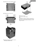
Page 85: ...21 Exploded Views 21 1 Cabinet Parts Location SA AK340P SA AK340PC 85 ...

Page 86: ...SA AK340P SA AK340PC 86 ...

Page 87: ...SA AK340P SA AK340PC 87 ...

Page 88: ...21 2 Packaging SA AK340P SA AK340PC 88 ...

Page 89: ...MB0312 TRIGGER LEVER SPRING M 111 RMB0400 REEL SPRING M 112 RMB0403 HEAB PANEL SPRING M 113 RMB0404 BRAKE ROD SPRING M 114 RMB0406 5 FR LEVER SPRING M 115 RMB0408 THRUST SPRING M 116 RML0370 4 TRIGGER LEVER M 117 RML0371 FR LEVER M 118 RML0372 2 WINDING LEVER M 119 RML0374 2 EJECT LEVER M 120 RMM0131 1 BRAKE ROD M 121 RMM0133 1 EJECT ROD M 122 RMQ0519 REEL HUB M 123 RMS0398 1 MOVING CORE M 124 RSJ...

Page 90: ...NSISTOR M Ref No Part No Part Name Description Remarks Q1003 B1AAGC000007 TRANSISTOR M Q1004 B1AAGC000007 TRANSISTOR M Q1005 B1AAGC000007 TRANSISTOR M Q1007 B1ABCF000176 TRANSISTOR M Q1017 B1AARC000003 TRANSISTOR M Q2142 B1ABCF000176 TRANSISTOR M Q2242 B1ABCF000176 TRANSISTOR M Q2311 B1ABCF000176 TRANSISTOR M Q2317 B1ABCF000176 TRANSISTOR M Q2341 B1ABCF000176 TRANSISTOR M Q2411 B1ABCF000176 TRANSI...

Page 91: ...6203 EVQ21405RJ SW DECK 1 2 M S6204 EVQ21405RJ SW H BASS M Ref No Part No Part Name Description Remarks S6205 EVQ21405RJ SW FF M S6206 EVQ21405RJ SW REW M S6207 EVQ21405RJ SW DECK 1 OPEN M S6301 EVQ21405RJ SW CD M S6302 EVQ21405RJ SW TAPE M S6303 EVQ21405RJ SW STOP M S6304 EVQ21405RJ SW REC M S6305 EVQ21405RJ SW TUNER BAND M S6306 EVQ21405RJ SW MUSIC PORT M S6308 EVQ21405RJ SW MULTI DISC CHANGE M ...

Page 92: ... 390 1 4W M R10 D0AE391JA048 390 1 4W M R11 ERDS2TJ684T 680K 1 4W M R952 ERDS2TJ821T 820 1 4W M R953 ERDS2TJ393T 39K 1 4W M R972 ERDS2TJ821T 820 1 4W M R973 ERDS2TJ393T 39K 1 4W M R1002 ERJ3GEY0R00V 0 1 16W M R1003 ERJ3GEYJ103V 10K 1 16W M R1004 D0GB152JA007 1 5K 1 16W M R1005 D0GB472JA041 4 7K 1 16W M R1007 ERD25FVJ4R7T 4 7 1 4W M R1009 D0GB183JA007 18K 1 16W M R1010 D0GB183JA007 18K 1 16W M R101...

Page 93: ... R2421 ERJ3GEY0R00V 0 1 16W M R2423 D0GB393JA007 39K 1 16W M R2426 ERJ3GEY0R00V 0 1 16W M Ref No Part No Part Name Description Remarks R2428 D0GB153JA007 15K 1 16W M R2429 D0GB332JA007 3 3K 1 16W M R2430 ERJ3GEY0R00V 0 1 16W M R2431 ERJ3GEY0R00V 0 1 16W M R2433 D0GB153JA007 15K 1 16W M R2434 ERJ3GEY0R00V 0 1 16W M R2435 ERJ3GEYJ102V 1K 1 16W M R2441 D0GB270JA007 27 1 16W M R2442 ERJ3GEY0R00V 0 1 1...

Page 94: ...6W M R2910 D0GB331JA007 330 1 16W M R2912 D0GB472JA041 4 7K 1 16W M R2914 D0GB472JA041 4 7K 1 16W M Ref No Part No Part Name Description Remarks R2916 D0GB472JA041 4 7K 1 16W M R2918 ERJ3GEYJ103V 10K 1 16W M R2919 D0GB472JA041 4 7K 1 16W M R2920 D0GB472JA041 4 7K 1 16W M R2921 D0GB472JA041 4 7K 1 16W M R2922 ERJ3GEYJ103V 10K 1 16W M R2923 ERJ3GEY0R00V 0 1 16W M R2924 ERJ3GEYJ103V 10K 1 16W M R2925...

Page 95: ...R6307 D0GB472JA041 4 7K 1 16W M R6308 ERJ3GEYJ682V 6 8K 1 16W M R6309 ERJ3GEYJ103V 10K 1 16W M Ref No Part No Part Name Description Remarks R6310 D0GB223JA041 22K 1 16W M R6399 ERJ3GEYJ103V 10K 1 16W M R6457 D0GB391JA041 390 1 16W M R6458 D0GB472JA041 4 7K 1 16W M R6481 ERJ3GEY0R00V 0 1 16W M R6491 D0GB473JA041 47K 1 16W M R6492 D0GB473JA041 47K 1 16W M R6493 ERJ3GEYJ103V 10K 1 16W M R6601 D0GB471...

Page 96: ...J3GEY0R00V CHIP JUMPER M W7025 ERJ3GEY0R00V CHIP JUMPER M W7026 ERJ3GEY0R00V CHIP JUMPER M W7027 ERJ3GEY0R00V CHIP JUMPER M W7028 ERJ3GEY0R00V CHIP JUMPER M K5101 B0EAKM000122 RECTIFIER M CAPACITORS Ref No Part No Part Name Description Remarks C1 F1D1H5R6A017 5 6P 50V M C2 F1D1H102A029 1000P 50V M C3 F1D1H2R2A017 2 2P 50V M C4 F1D1H181A012 180P 50V M C5 F1D1H5R6A017 5 6P 50V M C6 F1D1H3R3A017 3 3P...

Page 97: ...0P 50V M C2588 F1H1C104A041 0 1 16V M C2601 F1H1H103A219 0 01 50V M Ref No Part No Part Name Description Remarks C2602 ECA1CAK100XB 10 16V M C2603 F1H1H103A219 0 01 50V M C2604 F1H1H102A219 1000P 50V M C2606 F1H1H102A219 1000P 50V M C2607 ECJ1VB1E473K 0 047 25V M C2608 ECJ1VC1H080D 8P 50V M C2609 F1H1H102A219 1000P 50V M C2610 F1H1H103A219 0 01 50V M C2611 ECA1HAK4R7XB 4 7 50V M C2612 F1H1H103A219...

Page 98: ... C5335 ECJ1VB1H153K 0 015 50V M C5336 F1H1H102A219 1000P 50V M C5337 F1H1H102A219 1000P 50V M Ref No Part No Part Name Description Remarks C5343 ECJ1VB1H153K 0 015 50V M C5401 ECJ1VB1A474K 0 47 10V M C5402 F1H1H331A013 330P 50V M C5403 ECJ1VB1A474K 0 47 10V M C5404 ECJ1VB1A474K 0 47 10V M C5405 F1H1H331A013 330P 50V M C5406 ECJ1VB1A474K 0 47 10V M C5408 ECJ1VB1H104K 0 1 50V M C5409 ECJ1VB1H104K 0 ...

Page 99: ...C7228 ECA1HAK010XI 1 50V M C7230 ECJ1VB1C104K 0 1 16V M C7231 ECEA0JKA221I 220 6 3V M C7232 ECEA0JKA221I 220 6 3V M C7233 ECJ1VF1C104Z 0 1 16V M C7234 ECJ1VB1C104K 0 1 16V M C7235 ECEA1CKA100I 10 16V M C7241 ECJ1VB1H102K 1000P 50V M C7243 ECJ1VF1C104Z 0 1 16V M C7244 ECJ1VB1C153K 0 015 16V M C7253 ECJ1VB1H471K 470P 50V M C7263 ECJ1VB1C104K 0 1 16V M C7264 ECJ1VB1C104K 0 1 16V M C7315 ECJ1VB1A474K ...

Reviews: