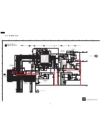
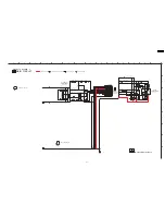
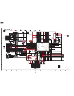
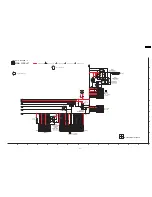
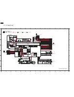
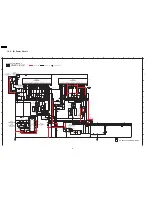
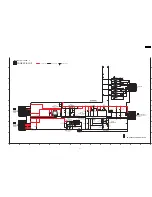
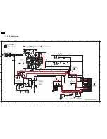
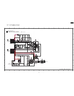
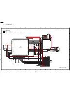
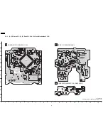
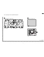
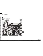
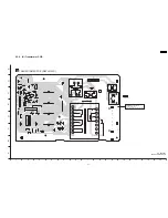

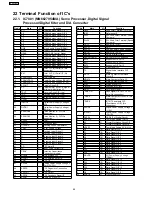
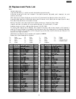
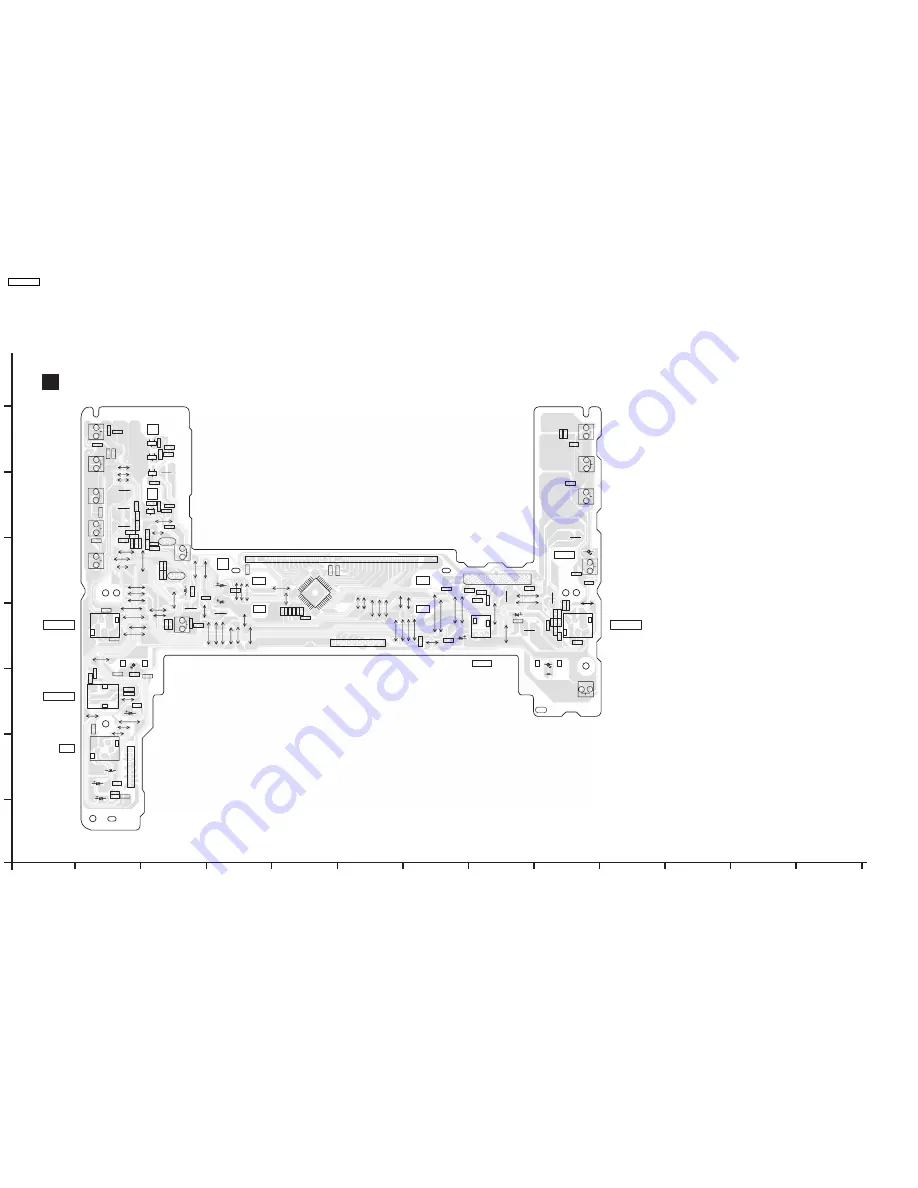
20.3. (C) Panel P.C.B.
1
2
3
4
5
6
7
8
9
A
B
C
D
E
F
G
H
10
1
12
13
C
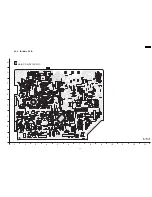
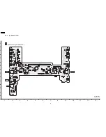
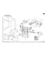
PANEL P.C.B (REPV0131E)
1
SA-AK450PL
PANEL P.C.B
PbF
C6632
R6109
C6631
H6555
C6552
JK6551
S6205
(CD5)
S6204
R6205
(CD4)
S6203
(CD3)
S6202
(CD2)
S6201
(CD1)
S6207
(/REW/)
S6206
(/FF/)
J6631
R6631
C6623
C6635
IC6601
JW6002
FL6602
C6481
Z6481
3
1
2
J6751
C6756
J6621
CN6601
S6105
(USB)
JK6751
J6752
S6101
(AC IN)
J6753
D6458
S6104
(SINGLE CHANGE)
S6102
(MULTI CHANGE)
(OPEN/CLOSE)
S6103
W831
W832
W1015
W801
W903
W808
W833
W871
W835
W872
W891
W837
W836
W838
W803
W842
W841
W809
W808
W807
R6202
W873
W910
W840
W1017
W1
103
W802
W834
W1010
W874
W875
W877
W810
W913
W845
W878
W876
W843
W844
W847
W848
W81
1
W812
W846
W813
W814
W852
W853
W854
W882
W880
W881
W879
W816
W851
W815
W855
W856
W892
W893
W858
W860
W857
W859
W818
9
10
2
4
5
6
7
8
3
W908
W907
C6551
R6204
R6206
R6207
W924
W1011
W1012
W911
W909
W905
R
66
05
C6603
C6602
C6604
R6604
C6601
W915
W914
D6635
W925
D6301
R6763
R6753
R6754
R6458
C6636
C6753
R6751
W1005
W1002
W1001
R6601
R6603
R6602
R6102
R6105
R6103
R6104
R6209
R6208
R6199
W926
W904
R6481
R6493
R6203
C6553
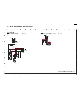
SENSOR
HEADPHONE
MUSIC PORT
0109A
0109A
R6632
QR6464
QR6463
QR6462
QR6461
Q6501
VR6511
MIC VOLUME
Q6502
JK6501
MIC
W1006
R6752
W1003
J6553
J6551
J6552
B
C
E
B
C
E
B
C
E
B
C
E
R6506
C6506
C6504
C6501
R6501
C6502
R6505
R6507
R6755
R6757
R6756
R6758
R6761
R6759
R6760
R6762
B
C
E
R6503
C6503
R6504
R6502
C6505
C6507
R6509
B
C
E
C6508
L6502
C6510
C6521
C6751
C6752
D6638
D6639
D6641
D6640
W901
W1004
W1000
C6509
L6501
W906
1
44
34
33
23
22
12
1
1
5
10
15
25
30
35
40
44
11
2
4
5
3
1
6
7
1
2
3
4
5
6
7
2
3
1
1
2
3
4
5
6
7
1
9
2
4
5
6
7
8
3
1
2
29
30
9
4
5
6
7
8
3
10 12 14 16 18 20 22 24 26 28
11 13 15 17 19 21 23 25 27
SA-AK450PL
80
Summary of Contents for SA-AK450PL
Page 8: ...8 SA AK450PL ...
Page 11: ...6 Accessories Remote Control FM Antenna Wire AC Cord AM Loop Antenna 11 SA AK450PL ...
Page 12: ...7 Operating Instructions Procedures 7 1 Main Unit Key Buttons Operations 12 SA AK450PL ...
Page 13: ...7 2 Remote Control Key Buttons Operations 13 SA AK450PL ...
Page 26: ...10 3 Main Parts Location 26 SA AK450PL ...
Page 38: ...10 17 1 Replacement of Pinch Roller and Head Block 38 SA AK450PL ...
Page 39: ...10 17 2 Replacement of Motor Capstan Belt A Capstan Belt B and Winding Belt 39 SA AK450PL ...
Page 45: ...12 4 Checking and Repairing of Power P C B 45 SA AK450PL ...
Page 47: ...47 SA AK450PL ...
Page 51: ...15 3 Main P C B 15 4 Panel P C B 51 SA AK450PL ...
Page 52: ...15 5 Power P C B Transformer P C B 52 SA AK450PL ...
Page 53: ...15 6 Waveform Chart 53 SA AK450PL ...
Page 62: ...SA AK450PL 62 ...
Page 64: ...64 SA AK450PL ...
Page 84: ...SA AK450PL 84 ...
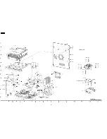
Page 89: ...23 Exploded Views 23 1 Cabinet Parts Location SA AK450PL 89 ...
Page 90: ...SA AK450PL 90 ...
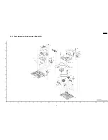
Page 91: ...23 2 Deck Mechanism Parts Location RAA4403 S SA AK450PL 91 ...
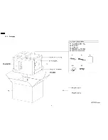
Page 92: ...23 3 Packaging SA AK450PL 92 ...