background image

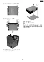
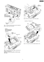
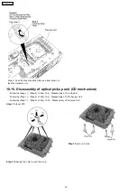
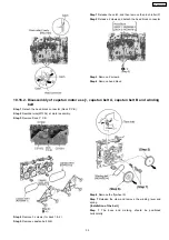
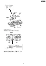
* The mechanism as shown below is for DECK1. For DECK
2, perform the same procedures.

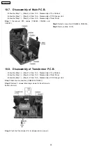
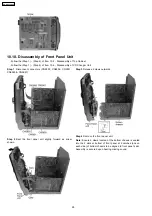
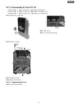
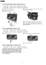
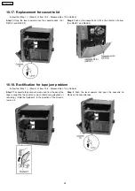
10.16. Disassembly of Deck Mechanism


·


Follow the (Step 1) - (Step 2) of Item 10.4 - Disassembly of Top Cabinet


·


Follow the (Step 1) - (Step 4) of Item 10.6 - Disassembly of CD Changer Unit


·


Follow the (Step 1) - (Step 4) of Item 10.10 - Disassembly of Front Panel Unit


·


Follow the (Step 1) - (Step 5) of Item 10.12 - Disassembly of Deck Mechanism Unit

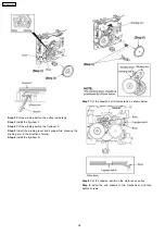
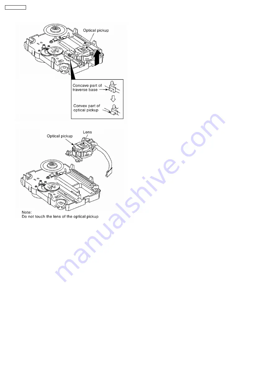
10.16.1. Disassembly of the pinch roller ass’y and head block

34

SA-AK640GCP

Summary of Contents for SA-AK640 GBP

Page 1: ... law SA AK640GCP Colour S Silver Type S N 20dB at 999 kHz 560 µV m Music Port input jack Terminal Stereo 3 5 mm jack Sensitivity 100 mV 4 7 kΩ Phone jack Terminal Stereo 3 5 mm jack Mic jack Terminal Mono 3 5 mm jack Sensitivity 0 7 mV 680 Ω n CASSETTE DECK SECTION Track system 4 track 2 channel Heads Record playback Solid permalloy head Erasure Double gap ferrite head Motor DC servo motor Recordi...

Page 2: ...x 330 x 343 mm Mass 7 1 kg Operating temperature range 5 to 35 C Operating humidity range 5 to 90 RH no condensation n SYSTEM SC AK640 GCP Music center SA AK640 GCP Speaker SB AK640 GC Subwoofer SB WAK640 GC For information on speaker system please refer to the original Service Manual Order No MD0512476A3 for SB AK640GC and Order No MD0512477A3 for SB WAK640GC Notes 1 Specifications are subject to...

Page 3: ...ain P C B 79 18 3 C Panel P C B 80 18 4 D Transformer P C B 81 18 5 E Power P C B 82 18 6 F Deck P C B G Deck Mechanism P C B H Tuner Pack P C B 83 19 Illustration of ICs Transistors and Diodes 85 20 Terminal Function of IC s 86 20 1 IC7001 MN6627954MA Servo Processor Digital Signal Processor Digital filter and D A Converter 86 20 2 IC7002 BA5948FPE2 IC 4CH Drive 87 20 3 IC2801 C2CBYY000066 System...

Page 4: ...part and measure the voltage at each point 5 Reverse the AC plug in the AC outlet and repeat each of the above measurements 6 The potential at any point should not exceed 0 75 volts RMS A leakage current tester Simpson Model 229 or equivalent may be used to make the hot checks leakage current must not exceed 1 2 milliamp Should the measurement is out of the limits specified there is a possibility ...

Page 5: ...ging ESD wrist strap which should be removed for potential shock reasons prior to applying power to the unit under test 2 After removing an electrical assembly equiped with ES devices place the assembly on a conductive surface such as aluminium foil to prevent electrostatic charge build up or exposure of the assembly 3 Use only a grounded tip soldering iron to solder or unsolder ES devices 4 Use o...

Page 6: ...short pin finish the job in as short time as possible 4 Do not turn the variable resistor for laser power adjustment It is pre adjusted during production time Grounding for electrostatic breakdown prevention 1 Human body grounding Use the anti static wrist strap to discharge the static electricity from your body 2 Work table grounding Put a conductive material sheet or steel sheet on the area wher...

Page 7: ...the preset variable resistor on the optical pickup lens 4 Do not disassemble the optical optical pickup unit 5 If the optical pickup is replaced use the manufacturer s specified replacement pickup only 6 Use of control or adjustments or performance of procedures other than those specified herein may result in hazardous radiation exposure CAUTION THIS PRODUCT UTILIZES A LASER USE OF CONTROLS OR ADJ...

Page 8: ...the melting point is 50 70 F 30 40 C higher Please use a high temperature soldering iron In case of soldering iron with temperature control please set it to 700 20 F 370 10 C Pb free solder will tend to splash when heated too high about 1100 F 600 C When soldering or unsoldering please completely remove all of the solder on the pins or solder area and be sure to heat the soldering points with the ...

Page 9: ...6 New Features 6 1 CRS1 Mechanism Overview 6 1 1 General Feature This is a five disc changer mechanism for CD DVD The outline figure is shown below 9 SA AK640GCP ...

Page 10: ... movement 6 1 3 Mechanism Operation This mechanism has the following state 1 Driving of a tray to open close 2 Up down operation of a traverse performs a state changes of tray By using the plunger to lift release of a switching gear and the cam gear to lift release the function gear the motor can be link to several gear trains to perform various operations The functions that can be perform in this...

Page 11: ...ollowing information for the mention CD Mechanism drive Schematic Diagram Block Diagram and P C B layout of CD Loading P C B Part List for individual parts of the mechanism Exploded View and Parts List for individual parts of the CD Mechanism drive Please refer to the original service manual Order No MD0509368C0 for the CD Mechanism Drive CRS1 6 2 Music Port 11 SA AK640GCP ...

Page 12: ...7 Accessories Remote Control FM Antenna Wire AC Cord AM Loop Antenna AC Plug Adaptor 12 SA AK640GCP ...

Page 13: ...8 Operating Instructions Procedures 13 SA AK640GCP ...

Page 14: ...14 SA AK640GCP ...

Page 15: ...of CD Changer Unit For more information refer to section 9 1 1 In Self Diagnostic Mode 1 Select for CD mode 2 Press button To exit press button on main unit or remote control The tray will return to PLAY position and then power off Doctor Mode To enter into Doctor Mode for checking of various items and displaying EEPROM and firmware version 1 2 1 All segments will light up for 1 second 2 The Check...

Page 16: ...nd LED will blink at 0 5 second interval In doctor mode 1 Press DIMMER button on remote control Tape Eject Test To check on the tape eject function For deck 1 2 In doctor mode 1 Press PROGRAM button on remote control 9 1 1 CD changer unit ageing test mode Below is the process flow chart of ageing for the CD changer unit CRS1 16 SA AK640GCP ...

Page 17: ...tion refer Section 9 1 provides information on any problems occuring for the unit and its respective components by displaying the error codes These error code such as U H and F are stored in memory and held unless it is cleared 17 SA AK640GCP ...

Page 18: ...turn Low a fail safe time after system command transmission is sent For CD unit For Traverse Press on main unit for next error F61 Power Amp IC output abnormal Upon power on PCONT HIGH DCDET L after checking LSI For power Press on main unit for next error IHMS Cam gear abnormality Cam gear does not rotate to HOME position For CD changer unit CRS1 Press SINGLE CHANGE on main unit for next error ICS...

Page 19: ...E CHANGE on main unit for next error UDU UD base asssembly abnormal UD Base assembly does not move upwards from tray 5 to tray 2 For CD changer unit CRS1 Press SINGLE CHANGE on main unit for next error UDD UD base asssembly abnormal UD Base assembly does not move downwards from tray 1 to tray 5 For CD changer unit CRS1 Press SINGLE CHANGE on main unit for next error UD1 UD base asssembly abnormal ...

Page 20: ...CRS1 Mechanism can be recalled and displayed in the order of the occurence under self diagnostic Refer to Section 9 1 for procedures to enter this mode Only the first 5 errors will be memorized in backup memory The subsequence error shall be ignored and not memorize For system with EEPROM as memory backup memory space in EEPROM is neccesary 2 To display all error code memorized In CRS1 Self Diagno...

Page 21: ...Special reassembly procedures are described only when required 3 Select items from the following index when checks or replacement are required 4 Refer to the Parts No on the page of Parts Location and Replacement Parts List Section 22 if necessary Warning This product uses a laser diode Refer to caution statement Precaution of Laser Diode Caution After replacing of CD Changer Unit ageing test is n...

Page 22: ...hart The following chart is the procedure for disassembling the casing and inside parts for internal inspection when carrying out the servicing To assemble the unit reverse the steps shown in the chart as below 22 SA AK640GCP ...

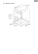
Page 23: ...10 3 Main Parts Location 23 SA AK640GCP ...

Page 24: ... 1 Remove 7 screws Step 2 Disconnect cable CN2810 Fan at Main P C B Step 3 Remove rear panel Step 1 Remove 1 screw at rear panel 10 4 Disassembly of Top Cabinet 10 5 Disassembly of Rear Panel Follow the Step 1 Step 2 of Item 10 4 Disassembly of Top Cabinet 10 6 Disassembly of CD Changer Unit CRS1 Follow the Step 1 Step 2 of Item 10 4 Disassembly of Top Cabinet 24 SA AK640GCP ...

Page 25: ...ards to remove it Disassembly of Mecha Chassis Step 5 Remove 2 screws Step 6 Remove the Mecha Chassis Note For disassembly assembly of traverse unit please refer to section 10 14 of this service manual Please refer to original Service Manual for the Disassembly and Assembly of the CD Changer Unit CRS1 25 SA AK640GCP ...

Page 26: ...N2808 CN2809 Step 3 Remove Main P C B Follow the Step 1 Step 2 of Item 10 4 Disassembly of Top Cabinet Follow the Step 1 Step 4 of Item 10 6 Disassembly of CD Changer Unit Follow the Step 1 Step 3 of Item 10 5 Disassembly of Rear Panel 10 8 Disassembly of Transformer P C B Follow the Step 1 Step 2 of Item 10 4 Disassembly of Top Cabinet Follow the Step 1 Step 3 of Item 10 5 Disassembly of Rear Pan...

Page 27: ... or 3 screws to Voltage Regulator Step 5 Cut the joints with a metal cutter as shown below Step 6 Desolder the terminals to replace the components Step 7 Fix back the cut portion with a screw as shown 10 9 Disassembly of Power P C B Follow the Step 1 Step 2 of Item 10 4 Disassembly of Top Cabinet Follow the Step 1 Step 4 of Item 10 6 Disassembly of CD Changer Unit Follow the Step 1 Step 3 of Item ...

Page 28: ... 2 claws located at the bottom chassis is seated into the 2 slots at bottom of front panel at 2 catches one on each side of bottom chassis to be aligned to front panel s slot Assembly is secured upon hearing clicking sound 10 10 Disassembly of Front Panel Unit Follow the Step 1 Step 2 of Item 10 4 Disassembly of Top Cabinet Follow the Step 1 Step 4 of Item 10 6 Disassembly of CD Changer Unit 28 SA...

Page 29: ...tep 1 Lift the spring sideward Step 2 Remove Lid Note Do not misplace the spring 10 11 Disassembly for Panel P C B Follow the Step 1 Step 2 of Item 10 4 Disassembly of Top Cabinet Follow the Step 1 Step 4 of Item 10 6 Disassembly of CD Changer Unit Follow the Step 1 Step 4 of Item 10 10 Disassembly of Front Panel Unit 29 SA AK640GCP ...

Page 30: ...te For disassembly of parts for deck mechanism unit refer to Section 10 15 Step 2 Desolder wire at deck motor terminals W1002 Step 3 Remove Deck P C B 10 12 Disassembly of Deck mechanism unit Follow the Step 1 Step 2 of Item 10 4 Disassembly of Top Cabinet Follow the Step 1 Step 4 of Item 10 6 Disassembly of CD Changer Unit Follow the Step 1 Step 4 of Item 10 10 Disassembly of Front Panel Unit 10 ...

Page 31: ...op Step 2 Push the traverse slide plate as arrow shown to release the traverse unit Caution Do not exert strong force on the traverse slide plate Step 3 Remove the traverse unit as arrow shown Assembly of Traverse Unit Step 1 Turn over the unit and install the traverse unit 31 SA AK640GCP ...

Page 32: ...he catch push the pin in Step 3 Remove 4 pins 10 15 Disassembly of optical pickup unit CD mechanism Follow the Step 1 Step 2 of Item 10 4 Disassembly of Top Cabinet Follow the Step 1 Step 4 of Item 10 6 Disassembly of CD Changer Unit Follow the Step 1 Step 2 of Item 10 14 Disassembly of Traverse Unit 32 SA AK640GCP ...

Page 33: ...rn it over Note Insert a short pin into FFC of the optical pickup Step 7 Rotate the traverse deck B to the arrow direction and shift the optical pickup to the furthest backward Step 8 Remove the catch of the drive rack and take out the drive rack Step 9 Place the convex part of an optical pickup to the concave part of a traverse base then take out the optical pickup 33 SA AK640GCP ...

Page 34: ... Step 2 of Item 10 4 Disassembly of Top Cabinet Follow the Step 1 Step 4 of Item 10 6 Disassembly of CD Changer Unit Follow the Step 1 Step 4 of Item 10 10 Disassembly of Front Panel Unit Follow the Step 1 Step 5 of Item 10 12 Disassembly of Deck Mechanism Unit 10 16 1 Disassembly of the pinch roller ass y and head block 34 SA AK640GCP ...

Page 35: ...en remove the pinch roller F Step 2 Release 2 claws and detach the head block connector Step 3 Remove 2 screws Step 4 Remove head block Step 6 Remove the flywheel R Step 7 Release the claw and remove the winding lever and spring Installation of the belt Step 1 The boss and marking should be positioned horizontally 10 16 2 Disassembly of capstan motor ass y capstan belt A capstan belt B and winding...

Page 36: ... Step 5 Install the winding lever and spring while pressing the winding arm in the direction of arrow Step 6 Install the flywheel R Step 7 Put the capstan belt A temporarily as shown below Step 8 Put the capstan belt B on the motor ass y pulley Step 9 Install the sub chassis to the mechanism and then tighten screws 36 SA AK640GCP ...

Page 37: ...Step 10 Install 3 screws Step 11 Put the capstan belt B as shown below Step 12 Put the capstan belt A on the motor ass y pulley 37 SA AK640GCP ...

Page 38: ...el F in the direction of the arrow to remove it Step 2 Push up the cassette lid L R in the direction of arrow For DECK1 and DECK2 Step 2 Push the lever upward and open the cassette lid Remove the cassette tape 10 17 Replacement for cassette lid Follow the Step 1 Step 2 of Item 10 4 Disassembly of Top Cabinet 10 18 Rectification for tape jam problem Follow the Step 1 Step 2 of Item 10 4 Disassembly...

Page 39: ...sion FFC A Deck P C B Main P C B REEX0485 14 Pins B Panel P C B Deck Mechanism P C B REEX0484 10 Pins 12 Service Positions Note For description of the disassembly procedures see the Section 10 12 1 Checking and Repairing of Main P C B 39 SA AK640GCP ...

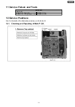
Page 40: ...12 2 Checking and Repairing of Transformer P C B 40 SA AK640GCP ...

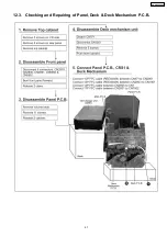
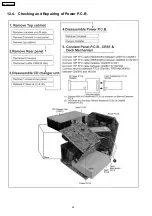
Page 41: ...12 3 Checking and Repairing of Panel Deck Deck Mechanism P C B 41 SA AK640GCP ...

Page 42: ...12 4 Checking and Repairing of Power P C B 42 SA AK640GCP ...

Page 43: ...e output frequency of the DECK 1 FWD are within 60 Hz of the value of the output frequency of DECK 2 FWD Fig 1 13 1 2 Bias Voltage Check 1 Set the unit AUX position 2 Insert the Normal blank tape QZZCRA into DECK 2 and the unit to REC mode use l REC STOP key 3 Measure and make sure that the output is within the standard value Bias voltage for Deck 2 14 4mV Normal Fig 2 Fig 3 13 Adjustment Procedur...

Page 44: ...ut frequency is maximized at 450kHz in Fig 6 Fig 5 Fig 6 13 2 2 AM RF Adjustment 1 Set up the equipments as shown in Fig 7 2 Select TUNER on selector and set to AM mode 3 Set AM SG to 520kHz 4 Receive 520kHz in the unit 5 Adjust L2601 OSC so that the EVM AC is maximized 6 Set AM SG to 600Hz 7 Receive 600Hz in the unit 8 Adjust L2601 ANT so that the EVM SG is maximized 9 Set AM SG to 520kHz 10 Rece...

Page 45: ...Fig 7 13 2 3 Adjustment Point Below is the locations of alignment points on the Main Tuner P C B 45 SA AK640GCP ...

Page 46: ...ribed herein shall be regarded as reference information when probing defect point because it may differ from an actual measuring value due to difference of Measuring instrument and its measuring condition and product itself 14 1 CD Servo P C B Main P C B 46 SA AK640GCP ...

Page 47: ...47 SA AK640GCP ...

Page 48: ...14 2 Power P C B Transformer P C B 48 SA AK640GCP ...

Page 49: ...14 3 Waveform Chart 49 SA AK640GCP ...

Page 50: ...50 SA AK640GCP ...

Page 51: ...DER SIDE SOLDER SIDE B MAIN P C B FM ANT AM ANT JK2601 H TUNER PACK P C B TUNER PACK PbF CN2809 1 12 1 12 CN2808 CN2803 14 2 13 1 CN2951 10 2 9 1 29 1 30 2 CN2806 CN2805 JK5102 JK5101 1 15 2 14 1 2 17 16 CN2801 1 2 To Fan CN2810 FAN MOTOR 2 1 BLACK RED SENSOR Z6481 JK6551 JK6751 VOLUME VR6491 CN6601 30 2 29 1 E POWER P C B SOLDER SIDE LEFT SPEAKER SUB WOOFER RIGHT SPEAKER H5104 W5104 9 1 CN5103 1 ...

Page 52: ...52 SA AK640GCP ...

Page 53: ...F LD RST LPD ARFF PC SPOUT TRVP TRP FOP ARFOUT ARFDC RFOUT RFIN CENV CTRCRS OSCIN VREF RFENV PC SPOUT TRVP TRP FOP LD PD A B C D E F NSRVMONON NTEST2 MDATA ARFIN ARFF BLKCK IREF DSLF PLLF PLLFO TXTCK SBCK PRAMVDD33 PRAMVSS33 D0 D15 A0 A11 BA0 BA1 TXTD DQSY SUBC TXNCLDCK BLKCK FLAG 65 71 20 18 83 92 94 99 1 7 11 15 16 17 NWE NCAS 8 9 63 64 62 NRAS SDRCK LRCK BCLK SRDATA EXT0 EXT2 EXT1 10 100 DVDD2 ...

Page 54: ...OOF RECH L1002 IC951 PHOTO INTERRUPTER CNB13030R2AU 97 PHOT0_1 6 19 15 12 21 4 22 3 17 8 1 2 24 23 3 5 2 4 Q2980 DECK MOTOR SWITCH M1002 S951 MODE 52 HALF_1 53 MODE_1 S952 HALF Z971 INTERFACE 91 DECK2 S972 HALF S975 RECINH_F S971 MODE DECK 2 R P HEAD LCH Q1017 MOTOR SWITCH M DECK 2 ERASE HEAD DECK 1 P B HEAD LCH MLD MCLK CE MDATA SD BLKCK PLLCLK ST DO RST STAT B CD_RST JOG VOL VR6491 IC2801 C2CBYY...

Page 55: ...ER CONTROL SWITCH MUTING CONTROL MUTING CONTROL MUTING CONTROL AGC CONTROL SWITCH Q2511 Q2411 Q2311 Q2142 Q2242 DATA 40 CLK 39 26 ASP_DAT 27 ASP_CLK 47 DCDET IN L1 R1 IN L3 R3 IN L2 R2 1 2 3 4 REC L R 53 17 REC L R 55 REC L R 56 GV OUT L R 54 16 IN_L4 R4 7 8 5 6 42 37 L OUT R OUT D2503 20 SYNC 7 F_HOP F_HOP 6 STANDBY STANDBY F_HOP SYNC 46 PCONT EFP_ CE PCONT EFP_ CE PCONT EFP_ CE KEY3 92 94 KEY1 D...

Page 56: ...BLISER LIMITER SWITCH 11V VOLTAGE REGULATOR Q5101 Q5110 Q5111 FP5920 Q5102 Q5108 Q5109 Q2950 Q2952 C1BA00000407 2 CH DIGITAL AMP IC5301 11 13 VSSP1 2 8 16 VDDP1 2 IN1 IN1 2 3 IN2 21 IN1 3 IN2 21 IN2 22 OSC 1 MODE BOOT1 OUT1 L5301 BOOT2 OUT2 23 9 10 15 16 C1BA00000407 2 CH DIGITAL AMP IC5401 11 13 VSSP1 2 8 16 VDDP1 2 IN1 2 IN2 22 OSC 1 MODE BOOT1 OUT1 L5401 BOOT2 OUT2 23 9 10 15 16 IN1 3 IN2 21 C1...

Page 57: ...e voltage value and waveforms are the reference voltage of this unit measured by DC electronic voltmeter high impedance and oscilloscope on the basis of chassis Accordingly there may arise some error in voltage values and waveforms depending upon the internal impedance of the tester or the measuring unit Importance safety notice Components identified by mark have special characteristics important ...

Page 58: ...58 SA AK640GCP ...

Page 59: ...7 0 C7315 0 47 R7323 3 3K R7327 1K R7335 100 C7335 0 1 C7334 10V220 R7336 10 F C7670 0 1 C7626 0 1 R7315 3 3K R7325 330 IC7002 BA5948FPE2 4 CH DRIVE VCC NC NC NC IN3 IN4 VREF NC GND GND PVCC2 PGND2 D4 D4 D3 D3 PGND1 PVCC1 NC D2 D2 D1 D1 IN1 NC NC PC2 PC1 IN2 NC 3 4 5 6 24 25 26 27 28 8 1 2 23 21 9 20 10 19 1 11 18 2 13 17 16 15 22 7 14 R7339 1K A 12 11 10 2 4 6 8 9 7 5 3 1 13 14 15 16 CN7001 CP701...

Page 60: ...SA AK640GCP 60 ...

Page 61: ...615 50V4 7 C2616 0 033 R2620 47K R2643 22K C2638 0 01 R2623 68K C2620 16V10 R2621 22K R2602 4 7K C2639 50V4 7 C2618 0 01 C2617 0 01 C2642 50V1 R2642 6 8K C2641 50V1 R2641 6 8K R2626 1K R2625 470 R2629 27K R2627 470 C2624 100P R2632 10K C2648 0 01 R2624 33 X2602 H3F1065A0002 C2622 50V1 R2622 2 7K C2621 50V0 47 R2631 120 R2644 120 R2633 W2919 0 1K C2629 6 3V100 C2649 0 1 C2623 50V1 R2645 100K C2643 ...

Page 62: ...SA AK640GCP 62 ...

Page 63: ... IN R6 GND REF IN REF OUT REC_L PRE VIN R HB MIX IN HB MIX OUT HB FLT OUT HB ATT IN HB ATT OUT HB LPF IN HB LPF OUT NC NC TRE R MID R1 MID R2 BASS R2 T OUT R R OUT VCC CLK DATA NC L OUT POST VM L T OUT L BASS L2 BASS L1 MID L2 MID L1 TRE L SUR2 SUR1 REC L SV_OUT L OP OUT OP IN PRE VIN L POST VM R BASS R1 HARMIN HARMOUT GV OUT R IN L2 IN L3 IN L4 IN L5 IN L6 C2214 1 C2114 1 R2704 220K C2704 470P FM...

Page 64: ... 2K R2326 0 R2317 10K R2356 180K R2456 180K R2417 10K C2343 0 47 C2443 0 47 R2416 2 2K C2321 0 22 R2318 100K R2418 100K 1 2 3 4 5 6 7 8 9 10 11 12 HIGH_L IN 15V MUTE D AMP T GND F_HOP CN2809 A_GND LOW_R IN FAN LOW_L IN ASP_GND HIGH_R IN Q2341 Q2441 R2345 1 5K R2445 1 5K R2357 100K R2457 100K C2344 0 47 C2444 0 47 R2447 1 R2446 3 3K R2346 3 3K R2347 1 R2451 0 C2943 50V2 2 R2453 0 R2452 27 R2454 27 ...

Page 65: ...A_IN_GND PA_IN_R MOT10V SW_LED VOL_LED J_VOLA J_VOl_B FL_RST FL_CS FL_DOUT FL_CLK H_BASS_LED KEY3 KEY2 KEY1 P GND RMT VREF SYNC PCONT SYS6V 15V MOT_12V CHG_PLR 88 HP_L HP_GND HP_R UP_GND SW5V PA_IN_L PA_IN_GND PA_IN_R MOT_12V SW_LED VOL_LED J_VOLA J_VOl_B FL_RESET FL_CS FL_DOUT FL_CLK H_BASS_LED KEY3 KEY2 KEY1 P GND RMT VREF SYNC PCONT SYS6V 1 2 3 4 5 6 7 8 9 10 11 12 14 16 17 18 19 20 21 22 23 24...

Page 66: ...100K R2817 100K R2830 100K R2831 100K R2832 100K R2833 100K R2810 22K R2802 100 C2821 100P R2882 10M R2883 330K C2883 18P R2886 1M R2881 220 C2803 1 C2853 0 1 R2851 47K C2940 0 1 R2940 820K D2803 B0ACCK000005 D2801 B0ACCK000005 C2802 50V3 3 C2882 18P X2801 H0A327200115 X2802 H2B100500004 R2803 10K VREF R2873 22K R2871 22K R2874 4 7K C2871 330P C2874 330P C2872 0 022 1 2 3 4 8 7 6 5 NC VCC EE_CS EE...

Page 67: ...V 15V GND2 VREF HP_SW GND2 KEY3 KEY1 R6102 1K GND2 SYNC PCONT SYS6V FL6602 A2BD00000142 5 6 7 8 9 10 1 12 13 14 15 16 17 18 19 20 21 22 23 24 25 26 27 28 29 30 31 32 33 34 35 36 37 38 39 40 88 87 84 83 82 81 80 79 78 77 76 75 74 73 72 71 70 69 68 67 66 65 64 63 62 61 60 59 58 57 56 55 54 53 52 51 50 49 46 45 1 2 3 4 5 6 8 7 9 S6101 POWER S6102 SINGLE DISC CHANGE R6103 2 2K S6103 OPEN CLOSE R6104 1...

Page 68: ...SA AK640GCP 68 ...

Page 69: ... 50V4 7 R5958 10K R5957 10K C5954 0 01 JK5950 FL2 VP FL1 SYS6V SYS6V PCONT SYNC D_GND TO POWER CIRCUIT H5104 W5104 ON SCHEMATIC DIAGRAM 6 TO PANEL CIRCUIT H6555 W6555 ON SCHEMATIC DIAGRAM 4 Q5951 2SB0621AHA Q5952 Q5952 B1GACFJJ0018 SYNCHRONISATION SWITCH T5951 RTP1H3E002 C5960 D5952 D5950 D5951 D5953 0 1 D5970 D5973 B0EAMM000038 D5972 D5970 D5971 D5973 D5954 D5955 D5956 D5957 C5959 0 01 Z5950 ERZV...

Page 70: ...SA AK640GCP 70 ...

Page 71: ... SIGNAL LINE Q5201 B1ABCF000176 FREQUENCY HOPPING SWITCH Q5202 B1ADCF000063 FREQUENCY HOPPING SWITCH Q5111 B1BACG000023 15V REGULATOR Q5103 Q5104 B1ABCF000176 FAN ON OFF SWITCH IC5301 C1BA00000407 2 CH DIGITALAMP IC5401 C1BA00000407 2 CH DIGITALAMP IC5501 C1BA00000407 2 CH DIGITALAMP Q5154 2SB0709AHL PCONT SWITCH Q5173 B1ABCF000176 SWITCH Q5153 B1ABCF000176 MODE SWITCH W5504 0 W5507 0 C5335 0 022 ...

Page 72: ...0K VCC 6A 6Y 5A 5Y 4A 4Y 1A 2A 1Y 2Y 3A 3Y GND C5434 0 022 C5334 C5438 0 022 C5537 0 022 C5536 0 022 0 022 R5412 220K R5513 330K R5512 270K R5317 10K R5417 10K R5312 56K 2 4 5 6 1 JK5102 L_LOW SW SW L_LOW L_HIGH L_HIGH 3 R5406 22 C5424 0 68 C5427 0 68 R5405 22 C5432 220P C5430 220P C5425 0 1 C5426 0 C5428 0 1 C5429 0 R5407 10 R5408 10 2 3 1 4 C5117 35V470P C5118 35V470P C5431 220P C5433 220P L5403...

Page 73: ...303 5 6K R5304 5 6K C5306 0 47 C5336 1000P C5305 330P C5301 0 47 R5301 5 6K R5302 5 6K C5303 0 47 C5337 1000P C5302 330P 2 3 1 4 HL_R LQ_R AGND AGND MOD AGN C5330 220P C5332 220P C5123 35V470P C5124 35V470P L5101 J0JKB0000037 L5102 J0JKB0000037 R5112 47K R5113 47K CN5103 TO MAIN CIRCUIT CN2808 ON SCHEMATIC DIAGRAM 3 1 2 3 4 5 6 7 8 9 10 11 12 PGND FLGND DGND PCONT CD8V NC STANDBY 12V 15V 3V SW5V D...

Page 74: ...000P C5302 330P 2 3 1 4 HL_R LQ_R AGND AGND C5330 220P C5332 220P C5123 35V470P C5124 35V470P L5101 J0JKB0000037 L5102 J0JKB0000037 R5112 47K R5113 47K CIRCUIT SA AK640GCP POWER CIRCUIT E5103 K4CZ01000027 E5101 K4CZ01000027 Q5201 B1ABCF000176 FREQUENCY HOPPING SWITCH Q5202 B1ADCF000063 FREQUENCY HOPPING SWITCH Q5115 AAKD000014 7 REGULATOR Q5114 B1ABCF000176 11V REGULATOR Q5112 B1BCCG000002 CURRENT...

Page 75: ...47 C1008 50V1 C1034 50V3 3 R1032 10K R1055 2 2K C1038 220P C1042 16V22 R1031 27K R1035 10K R1030 100 5 11 12 TAPE B INPUT TAPE B INPUT TAPE A INPUT TAPE A INPUT PB AMP NF PB AMP NF PB AMP EQ PB AMP EQ PB AMP OUTPUT PB AMP OUTPUT AB SW T REC IN REC IN REC OUT REC OUT REC PB SW AB SW RIPPLE FILTER OUTPUT GND VCC CRO NOR HI LO ALC T ALC LOW CUT IC1001 SW GND CTRL2 CTRL1 3 C1058 1000P R1100 0 R1101 0 ...

Page 76: ...SA AK640GCP 76 ...

Page 77: ...18 Printed Circuit Board Note Circuit board diagrams may be modified at any time with the development of new technology SA AK640GCP 77 ...

Page 78: ...3 W7028 C7243 TP4 X C7234 R7254 W7009 W7001 CN7002 W7010 C7235 W7011 TP3 X TP31 X TP1 X R7332 TP39 X TP10 X TP8 X TP7 X TP9 X M7301 TRV MOTOR TP38 X TP11 X TP36 X M7302 SPL MOTOR TP37 X R7335 R7325 R7315 TP2 X S7201 RESET SW C7264 R7214 R7220 X7201 C7263 C7166 C7230 C7216 R7212 W7013 C7241 C7217 R7211 C7244 W7012 C7223 C7203 W7014 W7015 C7204 TP51 RF C7161 C7102 C7142 C7107 IC7001 R7331 C7165 C731...

Page 79: ...02 C2275 C2195 C2194 R2195 R2196 R2194 C2193 R2271 C2272 C2271 R2273 C2274 C2273 R2587 C2633 C2634 X2603 IC2602 R2638 R2617 R2633 R2634 R2635 R2636 R2637 W2442 C2613 R2652 R2630 W2443 C2622 W2919 R2622 C2621 C2641 C2642 C2644 R2646 R2642 C2643 R2645 R2641 C2638 R2643 R2623 C2620 W2445 W2565 W2567 W2568 R2925 Q2907 B C E Q2906 W2291 W2290 W2293 W2288 K2904 W2297 W2296 W2292 W2294 W2295 W2570 W2569 ...

Page 80: ...032 W6024 W6041 W6028 W6019 W6006 W6005 W6015 W6034 W6033 W6036 W6014 W6012 W6043 W6010 W6020 W6027 W6063 W6037 W6402 W6082 W6085 W6102 W6101 W6100 W6081 W6080 W6072 W6073 W6074 C6491 C6492 C6551 C6552 C6553 C6601 C6602 C6603 C6604 C6636 C6753 D6635 R6102 R6103 R6104 R6105 R6106 R6107 R6108 R6109 R6110 R6199 R6202 R6203 R6204 R6205 R6206 R6207 R6208 R6302 R6303 R6304 R6305 R6306 R6307 R6308 R6399 ...

Page 81: ...Q5951 CN5951 W5923 W5922 W5906 W5904 CN5950 W5920 W5907 W5908 W5902 C5940 W5930 W5901 C5956 D5959 D5958 C5955 D5951 D5953 C5920 W5903 FP5920 10A FP5940 10A W5909 C5958 C5957 D5960 W5905 R5960 Q5953 R5961 D5966 C5954 C5952 R5963 D5964 C5953 Q5950 D5952 D5950 C5950 D5956 D5957 D5955 D5954 FP5950 4A W5910 C5960 D5965 SUB TRANSFORMER RL5950 Z5950 FC2 FC1 F1 250V 5A JK5950 W5914 W5915 W5916 W5917 AC IN...

Page 82: ...5306 R5304 W5507 C5437 W5150 C5337 W5149 C5401 R5401 R5404 W5506 C5406 C5404 R5403 W5133 L5401 W5156 L5402 R5135 R5136 R5137 D5109 C5113 R5134 W5508 Q5111 Q5114 Q5113 R5147 D5152 J5122 W5206 W5207 W5157 W5177 C5322 C5323 C5305 D5107 R5123 J5125 C5157R5126 R5127 C5110 C5109 L5101 C5318 C5123 W5169 W5163 W5152 W5153 W5154 W5155 W5175 R5518 W5161 CN5102 W5162 C5336 C5436 D5126 R5413 R5150 W5509 R5412...

Page 83: ...J1111 J1011 J1020 J1012 J1013 J1022 J1028 J1038 J1014 J1033 J1023 J1021 J1015 C1046 Q1005 R1007 W1002 CS1002 TO R P HEAD CS1001 TO P B HEAD L1002 IC1004 C1041 CN1001 J1010 J1004 C1030 C1032 C1045 C1033 C1037 C1056 C1031 C1035 C1042 J1064 J1051 L1001 Q1004 J1006 J9999 R1005 R1003 C1021 R1010 R1097 R1004 C1016 R1060 C1017 C1020 R1009 C1014 C1013 C1019 R1018 C1057 C1038 C1036 R1032 R1055 R1098 R1026 ...

Page 84: ...SA AK640GCP 84 ...

Page 85: ...3 B3ACA0000234 B0ADCC000002 B0BC5R000009 B0BC7R500001 Cathode Ca A Anode B0BC4R400016 B0BC9R000008 A Ca Cathode Anode C1BB00001121 100P C2CBYY000066 100P C0HBB0000039 44P MN6627954MA 100P 1 1 28 15 14 7 21 22 8 BA5948FPE2 A Ca Cathode Anode MAZ80560ML E C B E C B B1CECC000003 C1BA00000407 1 18 B0EAMM000038 A Ca Anode Cathode B0AACK000004 1 4 8 5 C0AABB000125 A Ca Cathode Anode B0EAKM000117 B0EAKM0...

Page 86: ...FB I ARF Feedback Signal I P 51 ARFIN I Audio RF Signal I P 52 DSLF I Loop Filter Terminal For DSL Pin No Mark I O Function 53 IREF I Reference I P 54 PLLF I PLL Loop Filter Terminal Phase Compare 55 PLLF0 O PLL Loop Filter Terminal Speed Compare 56 OUTL O Audio O P LCH 57 AVSS1 GND 58 AVDD1 I Analog Power Supply Voltage 1 59 OUTR O Audio O P RCH 60 DVSS3 GND3 Digital Circuit 61 NSRVMONON I Servo ...

Page 87: ...o Mute 41 EE_CS EFP EPH O EEPROM Chip Select 42 EE_CLK O EEPROM CLOCK Pin No Mark I O Function 15 D3 O Motor Drive 3 reverse action output 16 D3 O Motor Drive 3 forward action output 17 D4 O Motor Drive 4 reverse action output 18 D4 O Motor Drive 4 forward action output 19 PVCC2 Power Supply 2 for Driver 20 PGND2 Ground Connection 2 for Driver 21 24 N C O No Connection 25 VCC I Power Supply termin...

Page 88: ...for CRS1 90 UP_SENSOR I UD Sensor for CRS1 91 DECK2 I DECK CONDITION INPUT 2 R_INHF MODE2 HALF2 92 KEY3 I KEY3 INPUT 93 KEY2 I KEY2 INPUT 94 KEY1 I KEY1 INPUT 95 PHOTO_2 I Rotation Detection Signal Deck 2 96 AVSS Analog Power Supply Input Connect to GND 97 PHOTO_1 I Rotation Detection Signal Deck 1 98 VREF Reference for A D 5V 99 AVCC Analog Power Supply Input 100 DEMO I H default demo on L defaul...

Page 89: ...21 Exploded Views 21 1 Cabinet Parts Location SA AK640GCP 89 ...

Page 90: ...SA AK640GCP 90 ...

Page 91: ...21 2 Deck Mechanism Parts Location RAA4502 S SA AK640GCP 91 ...

Page 92: ...21 3 Packaging SA AK640GCP 92 ...

Page 93: ...4 MAIN GEAR M 107 RDV0033 4 WINDING BELT M 108 RDV0064 1 CAPSTAN BELT M 109 RDV0071 2 CAPSTAN BELT B M 110 RMB0312 TRIGGER LEVER SPRING M 111 RMB0400 REEL SPRING M 112 RMB0403 HEAD PANEL SPRING M 113 RMB0404 BRAKE ROD SPRING M 114 RMB0406 5 FR LEVER SPRING M 115 RMB0408 THRUST SPRING M 116 RML0370 4 TRIGGER LEVER M 117 RML0371 FR LEVER M 118 RML0372 2 WINDING LEVER M 119 RML0374 2 EJECT LEVER M 12...

Page 94: ...2 B1AAAC000016 TRANSISTOR M Q3 B1AAAD000015 TRANSISTOR M Q4 B1AAAD000015 TRANSISTOR M Q1003 B1AAGC000007 TRANSISTOR M Q1004 B1AAGC000007 TRANSISTOR M Q1005 B1AAGC000007 TRANSISTOR M Q1007 B1ABCF000176 TRANSISTOR M Q1017 B1AARC000003 TRANSISTOR M Q2142 B1ABCF000176 TRANSISTOR M Q2242 B1ABCF000176 TRANSISTOR M Q2311 B1ABGC000005 TRANSISTOR M Q2317 B1ABGC000005 TRANSISTOR M Q2341 B1ABGC000005 TRANSIS...

Page 95: ...650 MAZ80560ML DIODE M Ref No Part No Part Name Description Remarks VARIABLE RESISTORS VR6491 EVEKE2F3524B VR VOLUME JOG M VR6511 EVUF2AF15B14 VR MIC VOLUME JOG M SWITCHES S951 K0J1BB000017 SW MODE M S952 K0J1BB000021 SW HALF M S971 K0J1BB000017 SW MODE M S972 K0J1BB000021 SW HALF M S975 K0J1BB000021 SW RECINH_F M S5950 K0ABLB000003 SW VOLTAGE SELECTOR M S6101 EVQ21405RJ SW POWER M S6102 EVQ21405R...

Page 96: ...TERMINALS E5101 K4CZ01000027 EARTH LUG M E5103 K4CZ01000027 EARTH LUG M WIRES W1002 RWJ0102050CK MAIN TO MECHA MOTOR M W5104 REXX0325 9P FLAT WIRE M W6555 REXX0324 9P FLAT WIRE M PACKING MATERIALS P1 RPGX1532 PACKING CASE M P2 RPNX0347 POLYFOAM M P3 RPFX0007 1 MIRAMAT BAG M ACCESSORIES A1 N2QAHB000064 REMOTE CONTROL M A1 1 RKK HTR0283H R C BATTERY COVER M A2 K2CQ2CA00006 AC CORD M A2 K2DA42E00001 ...

Page 97: ...A041 4 7K 1 16W M R2271 ERJ3GEYJ682V 6 8K 1 16W M R2273 D0GB472JA041 4 7K 1 16W M R2281 ERJ3GEYJ681V 680 1 16W M Ref No Part No Part Name Description Remarks R2282 ERJ3GEY0R00V 0 1 16W M R2283 D0GB104JA007 100K 1 16W M R2311 ERJ3GEYJ471V 470 1 16W M R2312 ERJ3GEYJ103V 10K 1 16W M R2313 D0GB104JA007 100K 1 16W M R2314 ERJ3GEY0R00V 0 1 16W M R2315 D0GB563JA007 56K 1 16W M R2316 D0GB222JA041 2 2K 1 1...

Page 98: ...R2676 ERJ3GEYJ103V 10K 1 16W M R2677 D0C1121JA020 120 1W M R2701 ERJ3GEYJ102V 1K 1 16W M Ref No Part No Part Name Description Remarks R2702 ERJ3GEYJ102V 1K 1 16W M R2703 D0GB224JA007 220K 1 16W M R2704 D0GB224JA007 220K 1 16W M R2705 D0GB332JA007 3 3K 1 16W M R2706 D0GB332JA007 3 3K 1 16W M R2721 ERJ3GEYJ102V 1K 1 16W M R2722 ERJ3GEYJ102V 1K 1 16W M R2731 D0GB101JA007 100 1 16W M R2801 ERJ3GEYJ103...

Page 99: ...W M R5202 D0GB104JA007 100K 1 16W M R5203 ERJ3GEYJ103V 10K 1 16W M R5204 D0GB104JA007 100K 1 16W M Ref No Part No Part Name Description Remarks R5205 D0GB104JA007 100K 1 16W M R5206 D0GB105JA007 1M 1 16W M R5207 ERJ3GEYJ682V 6 8K 1 16W M R5209 D0GB100JA007 10 1 16W M R5210 D0GB151JA007 150 1 16W M R5301 D0GB562JA007 5 6K 1 16W M R5302 D0GB562JA007 5 6K 1 16W M R5303 D0GB562JA007 5 6K 1 16W M R5304...

Page 100: ...Description Remarks W2520 ERJ3GEY0R00V CHIP JUMPER M W2523 ERJ3GEY0R00V CHIP JUMPER M W2525 ERJ3GEY0R00V CHIP JUMPER M W2526 ERJ3GEY0R00V CHIP JUMPER M W2530 ERJ3GEY0R00V CHIP JUMPER M W2531 ERJ3GEY0R00V CHIP JUMPER M W2532 ERJ3GEY0R00V CHIP JUMPER M W2534 ERJ3GEY0R00V CHIP JUMPER M W2535 ERJ3GEY0R00V CHIP JUMPER M W2536 ERJ3GEY0R00V CHIP JUMPER M W2537 ERJ3GEY0R00V CHIP JUMPER M W2539 ERJ3GEY0R00...

Page 101: ...H1H102A219 1000P 50V M C1059 F1H1H103A219 0 01 50V M C2101 ECJ1VB1A105K 1 10V M C2112 ECJ1VB1C105K 1 16V M Ref No Part No Part Name Description Remarks C2113 ECJ1VB1H682K 6800P 50V M C2114 ECJ1VB1C105K 1 16V M C2121 F1H1H332A013 3300P 50V M C2122 ECJ1VB1C105K 1 16V M C2124 ECJ1VB1C105K 1 16V M C2131 ERJ3GEY0R00V 0 1 16W M C2132 ECJ1VB1C105K 1 16V M C2134 ECJ1VB1C105K 1 16V M C2144 ECJ1VB1C105K 1 1...

Page 102: ...50V M C2648 F1H1H103A219 0 01 50V M C2649 F1H1C104A008 0 1 16V M C2671 ECJ1VC1H101K 100P 50V M Ref No Part No Part Name Description Remarks C2673 ECJ1VC1H101K 100P 50V M C2674 F1H1H103A219 0 01 50V M C2678 F1H1H103A219 0 01 50V M C2701 F1H1H103A219 0 01 50V M C2702 ECA1CAK101XB 100 16V M C2703 F1H1H471A219 470P 50V M C2704 F1H1H471A219 470P 50V M C2705 ECA1HAK010XB 1 50V M C2706 ECA1HAK010XB 1 50V...

Page 103: ...0P 100V M C5431 F1H2A221A009 220P 100V M C5432 F1H2A221A009 220P 100V M C5433 F1H2A221A009 220P 100V M Ref No Part No Part Name Description Remarks C5434 ECJ1VB1H223K 0 022 50V M C5435 ECJ1VB1H223K 0 022 50V M C5436 F1H1H102A219 1000P 50V M C5437 F1H1H102A219 1000P 50V M C5438 ECJ1VB1H223K 0 022 50V M C5501 ECJ1VB1A474K 0 47 10V M C5502 F1H1H331A013 330P 50V M C5503 ECJ1VB1A474K 0 47 10V M C5504 E...

Page 104: ...680P 50V M C7217 ECJ1VB1C104K 0 1 16V M C7218 ECJ1VB1C823K 0 082 16V M C7223 ECEA1HKA4R7I 4 7 50V M C7225 ECJ1VB1H102K 1000P 50V M C7226 ECJ1VB1H102K 1000P 50V M C7227 ECA1HAK010XI 1 50V M C7228 ECA1HAK010XI 1 50V M C7230 ECJ1VB1C104K 0 1 16V M C7231 F2A0J221A200 220P 6 3V M C7232 F2A0J221A200 220P 6 3V M C7233 ECJ1VF1C104Z 0 1 16V M C7234 ECJ1VB1C104K 0 1 16V M C7235 ECEA1CKA100I 10 16V M C7241 E...

Reviews: