background image

8.5.2.

CD Mechanism Error Code Table (CD Mechanism Unit (BRS1C))

8.6.

Sales Demonstration Lock Function

8.6.1.

Entering into sales Demo Mode

Here is the procedures to enter into Sales Demonstration Lock.
Step 1: Turn on the unit.
Step 2: Select to any mode function.

Step 3: Press [

OPEN/CLOSE

] key then [ / ] key at the same time,press and hold both [

OPEN/CLOSE

] and [ / ] keys for 5 sec.

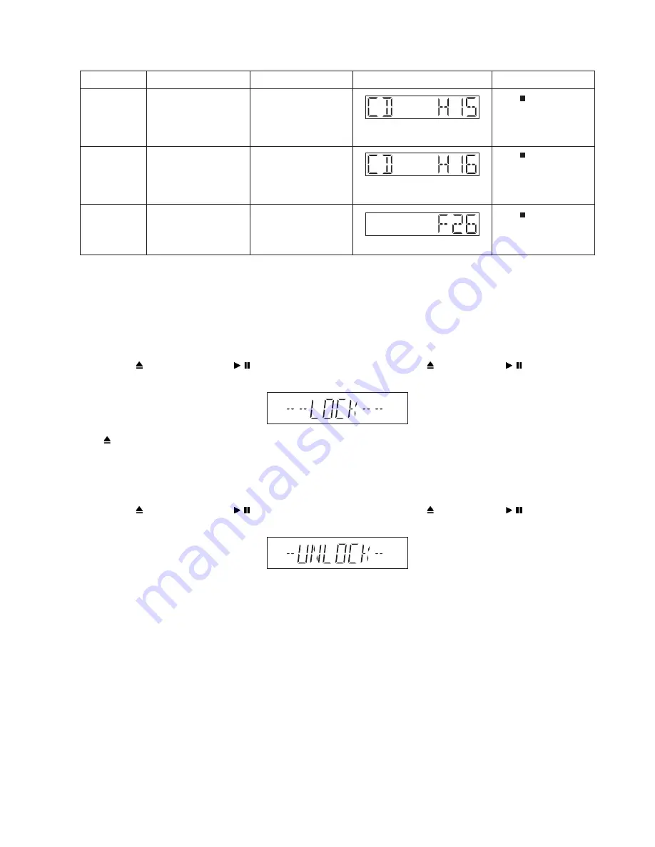
Step 4: The display will show upon entering into this mode for 2 sec..

Note: [

OPEN/CLOSE

] button is invalid and the main unit displays “LOCKED” while the lock function mode is entered.

8.6.2.

Cancellation

Step 1: Turn on the unit.
Step 2: Select to any mode function.

Step 3: Press [

OPEN/CLOSE

] key then [ / ] key at the same time,press and hold both [

OPEN/CLOSE

] and [ / ] keys for 5 sec.

Step 4: The display will show upon entering into this mode for 2 sec..

Error Code

Diagnostic Contents

Description of error

Automatic FL Display

Remarks

CD H15

CD Open Abnormal

During operation 
POS_SW_R On fail to be 
detected with 4 sec. Error 
No. shall be clear by force 
or during cold start.

Press [ ] on main unit for 
next error.

CD H16

CD Closing Abnormal

During operation 
POS_SW_CEN On fail to 
be detected with 4 sec. 
Error No. shall be clear by 
force or during cold start.

Press [ ] on main unit for 
next error.

F26

Communication between 
CD servo LSI and micro-p 
abnormal.

During switch to CD func-
tion, if SENSE = “L” within 
failsafe time of 20ms.

Press [ ] on main unit for 
next error.

24

Summary of Contents for SA-AKX14

Page 1: ...ying and distribution is a violation of law PMX1206001CE CD Stereo System Model No SA AKX14LM K Product Color K Black Type Please refer to the original service manual for CD Mechanism Unit BRS1C Order No PSG1102001CE Speaker system SB AKX14LM K Order No PMX1206002CE ...

Page 2: ...e Unit 3 Service Navigation 3 1 Service Information 4 Specifications 5 General Introduction 5 1 Media Information 6 Location of Controls and Components 6 1 Remote Control Key Button Operation 6 2 Main Unit Key Button Operation 7 Installation Instructions 7 1 Speaker and A C Connection 8 Service Mode 8 1 Cold Start 8 2 Doctor Mode Table Please refer to the original service manual for CD Mechanism U...

Page 3: ...nt of Regulator Diode D5803 11 20 Disassembly of CD Mechanism Unit BRS1C 11 21 Disassembly of Rear Panel 12 Replacement of Traverse Unit 12 1 Disassembly of Traverse Unit 12 2 Assembly of Traverse Unit 12 3 Disassembly of CD Servo P C B 13 Service Position 13 1 Checking and Repairing of Main P C B 13 2 Checking and Repairing of Panel P C B 13 3 Checking and Repairing of LCD P C B 13 4 Checking and...

Page 4: ...rs between each exposed metallic part on the set and a good earth ground such as a water pipe as shown in Figure 1 3 Use an AC voltmeter with 1000 ohms volt or more sensitivity to measure the potential across the resistor 4 Check each exposed metallic part and measure the voltage at each point 5 Reverse the AC plug in the AC outlet and repeat each of the above measurements 6 The potential at any p...

Page 5: ...e and negative speaker connection wires are shorted or if speaker systems with an impedance less than the indicated rated impedance of the amplifier are used If this occurs follow the procedure outlines below 1 Turn off the power 2 Determine the cause of the problem and correct it 3 Turn on the power once again after one minute Note When the protection circuitry functions the unit will not operate...

Page 6: ...without permission of manufacturer Modelo SC AKX14LM K INSTRUCTIVO RQTM0187 RKMX1011Z KL RD DDL081 PX F1BAF1020020 ERZV05Z471CS PCB SMPS F0CAF224A105 B3PBA0000579 RJB3568A 1 GAB MET SIN DOBLAR G0B612H00004 REAR PANEL CAPACITOR DE AC Numero de Parte Seguridad TRANSFORMADOR DE PODER TRANSFORMADOR DE RESPALDO CABLE TOMACORRIENTE CONECTOR TOMACORRIENTE OPTOACOPLADOR BRS1C CD UNIT BOBINA PRIMARIO FUSIB...

Page 7: ...the assembly 3 Use only a grounded tip soldering iron to solder or unsolder ES devices 4 Use only an anti static solder removal device Some solder removal devices not classified as anti static ESD protected can generate electrical charge sufficient to damage ES devices 5 Do not use freon propelled chemicals These can generate electrical charges sufficient to damage ES devices 6 Do not remove a rep...

Page 8: ...ion power from pickup 100 PW VDE Laser radiation from the pickup unit is safety level but be sure the followings 1 Do not disassemble the pickup unit since radiation from exposed laser diode is dangerous 2 Do not adjust the variable resistor on the pickup unit It was already adjusted 3 Do not look at the focus lens using optical instruments 4 Recommend not to look at pickup lens for a long time 8 ...

Page 9: ... used Definition The letter of PbF is printed on the PCB using the lead free solder To put lead free solder it should be well molten and mixed with the original lead free solder Remove the remaining lead free solder on the PCB cleanly for soldering of the new IC Since the melting point of the lead free solder is higher than that of the normal lead solder it takes the longer time to melt the lead f...

Page 10: ...pecial care must be taken avoid caution to electrostatic discharge damage when servicing the laser diode 1 Do not give a considerable shock to the optical pickup unit as it has an extremely high precise structure 2 To prevent the laser diode from the electrostatic discharge damage the flexible cable of the optical pickup unit removed should be short circuited with a short pin or a clip 3 The flexi...

Page 11: ...ic ity in the working environment Proceed servicing works under the working environment where grounding works is completed 2 4 2 1 Worktable grounding 1 Put a conductive material sheet or iron sheet on the area where the optical pickup is placed and ground the sheet 2 4 2 2 Human body grounding 1 Use the anti static wrist strap to discharge the static electricity form your body 11 ...

Page 12: ...f the circuit is changed or modified this information will be followed by supplement service manual to be filed with original service manual CD Mechanism Unit BRS1C 1 This model uses CD Mechanism Unit BRS1C Micro processor 1 The following components are supplied as an assembled part Micro processor IC IC2003 MN101EF16KXW Este material se encuentra sin programar necesita ser programado Speaker Syst...

Page 13: ... n á t s e B S U s o i d e m e d s o v i h c r a e d o t a m r o f n o c d a d i l i b i t a p m o C 3 P M 3 p m B S U o v i t i s o p s i d e d o v i h c r a e d a m e t s i S 2 3 T A F 6 1 T A F 2 1 T A F x á m A m 0 0 5 B S U o t r e u p a í g r e n E n ó i c c u d o r p e r s p b k 0 2 3 a s p b k 6 1 s t i b e d d a d i c o l e V o p i T as í v 2 e d as n i c o b 2 e d a m e t s i S s e v a r...

Page 14: ...5 General Introduction 5 1 Media Information 14 ...

Page 15: ...6 Location of Controls and Components 6 1 Remote Control Key Button Operation 15 ...

Page 16: ...6 2 Main Unit Key Button Operation 16 ...

Page 17: ...7 Installation Instructions 7 1 Speaker and A C Connection 17 ...

Page 18: ...is the procedure to carry out cold start or initialize to shipping mode 1 Unplug AC power cord 2 Press hold POWER button 3 Plug AC power cord while POWER button being pressed FL Display will show _ _ _ _ _ _ _ _ 4 Release POWER button 18 ...

Page 19: ... by 4 and 7 on remote control In CD mode 1 Enter Doctor Mode 2 To exit press DELETE button on remote control Displaying of 1 Year Develop 2 Model Type 3 ROM Type 4 Firmware Version 2 3 4 1 Version No 001 999 specific for each firmware Cold Start To active cold start upon next AC power up when reset start is execute the next time In Doctor Mode 1 Press SLEEP button on remote control or press POWER ...

Page 20: ...er to Section 6 3 Fig 2 for process flow The counter will increment by one When reach 9999 will change to 0000 Cancellation Display BRS1C Reliability Test Traverse To determine CD Mechanism BRS1C Access Inner Outer disc operation Note Refer to Section 6 3 Fig 3 for process flow The counter will increment by one When reach 9999 will change to 0000 Cancellation Display BRS1C Reliability Test Combina...

Page 21: ... 4 button on remote control Display of auto adjustment result Reference table ERROR Code Status Condition 0 1 2 4 6 8 A C E F AOC1 AOC2 O O O O O O O O ABC2 ABC1 O X O X O X O X 2nd AOC1 O O X X O O X X FAGC T AGC O O O O X X X X AGC2 O O O O O O O O O OK X NG In case that time out happens Either one of FO AOC TR AOC and FO coarse AGC is NG If theAGC is NG ignore others 2 To cancel press 0 on remo...

Page 22: ... 2 Reliability Test Traverse Fig 3 Reliability Test Combination OPEN Operation OPEN wait for 1 s CLOSE Operation CLOSE wait for 4 s Count up First Track Access First Track Play 5 s Last Track Access Last Track Play 5 s Count up First Track Access Access Play 10 s Open Operation Open wait for 1 s CLOSE Operation Count up First Track Last Track Last Track Play 10 s 22 ...

Page 23: ... Power Supply Error Code Table FL Display Key Operation Front Key Item Description Mode Name To enter into self diagnostic checking System will perform a check on any unusual error code from the memory To clear the stored in memory EEPROM IC Self Diagnostic Mode Error code information Delete error code Step 1 Select CD mode Ensure no disc is inserted Step 2 Press hold follow by on main unit for 2 ...

Page 24: ...ct to any mode function Step 3 Press OPEN CLOSE key then key at the same time press and hold both OPEN CLOSE and keys for 5 sec Step 4 The display will show upon entering into this mode for 2 sec Error Code Diagnostic Contents Descriptionof error Automatic FL Display Remarks CD H15 CD Open Abnormal During operation POS_SW_R On fail to be detected with 4 sec Error No shall be clear by force or duri...

Page 25: ... 1 1 SMPS P C B Fig 1 SMPS P C B Thermistor TH5860 Photocoupler PC5720 AC Inlet P5701 Fuse F1 Photocoupler PC5702 PC5799 Switching Regulator IC IC5701 SMPS Control IC IC5799 Main Transformer T5701 Rectifier Diode D5801 D5802 Connector CN5802 25 ...

Page 26: ... Circuit Q2022 Switching Voltage Regulator IC2011 Voltage Regulator Circuit D2004 Regulator Circuit Q2000 Regulator Circuit D2017 Voltage Regulator IC2009 Voltage Regulator Circuit IC2021 Resistor Defective R5905 Resistor Defective R5928 Resistor Defective R5936 Resistor Defective R5926 26 ...

Page 27: ...ii 3 3V Voltage Regulator IC2009 iii 9V Voltage Regulator Circuit Q2021 D2004 iv CD 7 5V Regulator Circuit Q2000 Q2022 D2017 3 P hotocoupler PC5720 solder crack PC5720 Dry joint short circuit open circuit 1 R ecti er Diode D580 Improper contact between D5801 to Heatsink Recti er Diode D5802 Improper contact between D5802 to Heatsink 2 T hermistor TH5860 1b Set trigger temperature protection Set ca...

Page 28: ... 3 D Amp IC Operation Control 28 ...

Page 29: ...1450 L 301 1460 1540 H 350 1550 1710 L 301 Table 4 F_HOP Control during 10 kHz Step Note During activating the 3 control pins namely MUTE_F MUTE_A and MODE_DA must be used to cover the Pop sound cause by F HOP switching 29 ...

Page 30: ...10 Service Fixture Tools Prepare service tools before process service position Ref No Service Tools Remarks SFT1 Main P C B CN2000 SMPS P C B CN5802 REX1534 15P Cable Wire 30 ...

Page 31: ...vice tools equipments or jigs is being used During replacement of component parts please refer to the section of Replacement Parts List as described in the ser vice manual Select items from the following indexes when disassembly or replacement are required Disassembly of Top Cabinet Disassembly of Tuner P C B Disassembly of Front Panel Unit Disassembly of Panel P C B Disassembly of Remote Sensor P...

Page 32: ...C B 11 5 Front panel Unit 11 6 Panel P C B 11 7 Remote Sensor P C B 11 8 USB P C B 11 9 LCD P C B 11 10 CD Lid 11 12 Voltage Regulator Transistor Q2022 11 13 Audio Digital Amp IC IC5902 11 14 SMPS P C B 11 15 Switching Regulator IC IC5701 11 16 Rectifier Diode D5702 11 17 Rectifier Diode D5801 11 18 Rectifier Diode D5802 11 19 Rectifier Diode D5803 32 ...

Page 33: ...11 2 Main Components and P C B Locations 33 ...

Page 34: ...p 3 Slightly pull both side of Top Cabinet outwards as arrow shown Step 4 Slightly lift up both side of Top Cabinet in an outward direction as shown Step 5 Remove the Top Cabinet Caution During assembling ensure that the Top Cabinet catches are properly located into Front Panel Unit as shown 34 ...

Page 35: ... Step 2 Detach 9P FFC at the connector CN51 on Tuner P C B Step 3 Remove the Tuner P C B 11 5 Disassembly of Front Panel Unit Refer to Disassembly of Top Cabinet Step 1 Detach 5P Cable Wire at the connector CN2005 on Main P C B Step 2 Detach 17P FFC at the connector CN2003 on Main P C B 35 ...

Page 36: ...ghtly at the Bottom Chassis as arrow shown and release tab at left side of Front Panel Unit Step 4 Release tabs at bottom Step 5 Push inwards slightly at the Bottom Chassis and release tab at right side of Front Panel Unit 36 ...

Page 37: ... the Front Panel Unit 11 6 Disassembly of Panel P C B Refer to Disassembly of Top Cabinet Refer to Disassembly of Front Panel Unit Step 1 Remove the Volume Knob Step 2 Remove the Skip Knob Step 3 Remove 6 screws 37 ...

Page 38: ... 1 10 Step 5 Lift up to remove the Panel P C B from Front Panel Unit Step 6 Desolder 7 pins at ZJ600A on Panel P C B Step 7 Remove the Panel P C B Caution During assembling ensure that Panel P C B is seated properly through the guides fully catched 38 ...

Page 39: ...Remote Sensor P C B Caution During assembling ensure that Remote Sensor P C B is properly inserted fully connected to Panel P C B 11 8 Disassembly of USB P C B Refer to Disassembly of Top Cabinet Refer to Disassembly of Front Panel Unit Refer to Step1 to Step5 of item 11 6 Step 1 Remove 1 screw Step 2 Remove the USB Unit Step 3 Release 1 catch Step 4 Remove the USB P C B 39 ...

Page 40: ...of Front Panel Unit Step 1 Remove 2 screws Step 2 Lift up the LCD Unit Step 3 Place the LCD P C B on an insulated material Step 4 Desolder 7 pins ZJ6000B on LCD P C B Step 5 Remove the LCD P C B Caution During assembling ensure that LCD Unit is prop erly located seated onto the guides 40 ...

Page 41: ...in order of sequence 1 to 3 Caution During assembling ensure that the spring is assembly at correct position Step 2 Remove CD Lid as arrow shown 11 11 Disassembly of Main P C B Refer to Disassembly of Top Cabinet Refer to Disassembly of Front Panel Unit Step 1 Detach 15P Cable Wire at the connector CN5802 on SMPS P C B Step 2 Remove 3 screws 41 ...

Page 42: ...ch 9P FFC at the connector CN2010 on Main P C B Step 6 Detach 27P FFC at the connector CN2706 on Main P C B Step 7 Detach 5P Wire CN2001 in Main P C B Step 8 Remove Main P C B Caution During assembling ensure that earth plate is bended flat against the Main P C B properly when inserted to locators 42 ...

Page 43: ... to its high tem perature after prolong use Touching it may lead to inju ries 11 12 2 Assembly of Voltage Regulator Transistor Q2022 Step 1 Apply grease to the Heatsink Step 2 Fix the Voltage Regulator Transistor Q2022 on Main P C B Caution Ensure pins of the Voltage Regulator Transistor Q2022 are properly seated on Main P C B Step 3 Screw the Voltage Regulator Transistor Q2022 to the Heatsink Cau...

Page 44: ...f 2 catches avoid touching the Heatsink due to high temperature Step 3 Remove Heatsink Clip Step 4 Remove Audio Digital Amp IC IC5902 11 13 2 Assembly of Audio Digital Amp IC IC5902 Step 1 Apply grease to the Heatsink Step 2 Fix the Audio Digital Amp IC IC5902 on Main P C B Caution Ensure pins of the Audio Digital Amp IC IC5902 are properly seated on Main P C B Step 3 Fix Heatsink Clip to the Heat...

Page 45: ...on the solder side of Main P C B 11 14 Disassembly of SMPS P C B Refer to Disassembly of Top Cabinet Refer to Disassembly of Front Panel Unit Step 1 Remove 1 screw Step 2 Remove 3 screws Step 3 Detach 15P Cable Wire at the connector CN5802 on SMPS P C B 45 ...

Page 46: ...aterial Step 6 Desolder 2 Wire pins TL7 Black TL8 Red Step 7 Remove SMPS P C B 11 15 Replacement of Switching Reg ulator IC IC5701 Refer to Disassembly of SMPS P C B 11 15 1 Disassembly of Switching Regula tor IC IC5701 Step 1 Desolder pins of the Switching Regulator IC IC5701 on the solder side of SMPS P C B 46 ...

Page 47: ...1 Apply grease to the Heatsink A Step 2 Fix the Switching Regulator IC IC5701 to the SMPS P C B Caution Ensure pins of the Switching Regulator IC IC5701 are properly inserted and soldered on SMPS P C B Step 3 Screw the Switching Regulator IC IC5701 to the Heat sink A Caution Ensure the Switching Regulator IC IC5701 is tightly screwed to the Heatsink A Step 4 Solder pins of the Switching Regulator ...

Page 48: ...e sol der side of SMPS P C B Step 2 Desolder pins of the Heatsink A Step 3 Remove 1 screw at Switching Regulator IC IC5701 Step 4 Remove the Heatsink A with Rectifier Diode D5702 Step 5 Remove 1 screw Step 6 Remove the Rectifier Diode D5702 from the Heatsink A Caution Avoid touching the Heatsink A due to its high temperature after prolong use Touching it may lead to injuries 48 ...

Page 49: ...f arrow Caution Ensure the Heatsink A with Rectifier Diode D5702 are properly seated on SMPS P C B Step 4 Screw the Switching Regulator IC IC5701 to the Heat sink A Caution Ensure that Switching Regulator IC IC5701 is tightly screwed to the Heatsink A Step 5 Solder pins of the Rectifier Diode D5702 on the solder side of SMPS P C B Step 6 Solder pins of the Heatsink A on the solder side of SMPS P C...

Page 50: ...1 from the SMPS P C B Caution Avoid touching the Heatsink B due to its high temperature after prolonged use Touching it may lead to injuries 11 17 2 Assembly of Rectifier Diode D5801 Step 1 Apply grease to the Heatsink B Step 2 Fix the Rectifier Diode D5801 on SMPS P C B Caution Ensure pins of the Rectifier Diode D5801 is properly inserted on SMPS P C B Step 3 Screw the Rectifier Diode D5801 to th...

Page 51: ... C B 11 18 1 Disassembly of Rectifier Diode D5802 Step 1 Desolder pins of the Rectifier Diode D5802 on the sol der side of SMPS P C B Step 2 Remove 1 screw at Rectifier Diode D5802 Step 3 Remove the Rectifier Diode D5802 from SMPS P C B Caution Avoid touching the Heatsink B due to its high temperature after prolong use Touching it may lead to injuries 51 ...

Page 52: ... 3 Screw the Rectifier Diode D5802 to the Heatsink B Caution Ensure the Rectifier Diode D5802 is tightly screwed to the Heatsink B Step 4 Solder pins of the Rectifier Diode D5802 on the solder side of SMPS P C B 11 19 Replacement of Regulator Diode D5803 Refer to Disassembly of SMPS P C B 11 19 1 Disassembly of Rectifier Diode D5803 Step 1 Desolder pins of the Rectifier Diode D5803 on the sol der ...

Page 53: ...1 19 2 Assembly of Rectifier Diode D5803 Step 1 Apply grease to the Heatsink B Step 2 Fix Rectifier Diode D5803 on SMPS P C B Caution Ensure pins of the Rectifier Diode D5803 are properly inserted on SMPS P C B Step 3 Screw the Rectifier diode D5803 to the Heatsink B Caution Ensure the Rectifier Diode D5803 is tightly screwed to the Heatsink B Step 4 Solder pins of the Rectifier Diode D5803 on the...

Page 54: ...to Disassembly of Top Cabinet Refer to Disassembly of Front Panel Unit Step 1 Detach 15P Cable Wire at the connector CN5802 on SMPS P C B Step 2 Remove 2 screws Step 3 Remove 3 screws Step 4 Detach Voltage Selector P C B from Rear Panel as arrow shown 54 ...

Page 55: ...er Chassis is catched onto Rear Panel properly Step 6 Remove 2 screws Step 7 Lift up upset the CD Mechanism Unit BRS1C as shown Step 8 Detach 27P FFC at the connector CN7002 on CD Servo P C B Step 9 Detach 5P Wire at the connector CN7001 on CD Servo P C B Step 10 Remove CD Mechanism Unit BRS1C 55 ...

Page 56: ...11 21 Disassembly of Rear Panel Refer to Disassembly of Top Cabinet Refer to Disassembly of Tuner P C B Step 1 Remove 6 screws Step 4 Release 2 tabs Step 5 Remove Rear Panel 56 ...

Page 57: ...al Pickup Unit Note 1 When the optical pickup unit is defective the overall traverse unit needs replacement 2 Please note that appropriate actions need to be taken to prevent static damage 3 Ensure that the circuit is open before assembly BRS1 to the main set Step 1 Use a pin to slide the Traverse Slide Plate until it come to a stop Step 2 Slide the tray out fully Step 3 Release the catches remove...

Page 58: ...e Slide Plate to the end Step 5 Detach 5P FFC at the connector CN7003 on CD Servo P C B Step 6 Lift the Traverse Unit by approximately 45q Step 7 Slide out the traverse unit as arrow shown Caution Avoid touching the surface of the Optical Pickup Unit 58 ...

Page 59: ...12 2 Assembly of Traverse Unit Step 1 Release the guide as shown slide the Traverse Slide Plate to the end Step 2 Slot the Traverse Unit at approximately 45q into the mecha chassis as arrow shown 59 ...

Page 60: ... Groove Step 4 Slide Traverse Slide Plate to lock the Traverse Unit as shown Step 5 Connect 5P FFC at the connector CN7003 on CD Servo P C B Step 6 Slide the Traverse Slide Plate unit it stop at the Guide Step 7 Slot the Tray into the guides as Picture shown 60 ...

Page 61: ...Slide the tray in fully 12 3 Disassembly of CD Servo P C B Refer to Disassembly of CD Mechanism Unit BRS1C Refer to Replacement of Traverse Unit Caution It is required to short the circuit Step 1 Solder the 3 solder points Caution 1 Avoid touching the surface of the Traverse Unit 61 ...

Page 62: ...ve 3 screws Step 3 Desolder 4 pins Step 4 Detach 5P FFC at the connector CN7003 on CD Servo P C B Step 5 Slightly lift up the CD Servo P C B Step 6 Flip the CD Servo P C B Step 7 Detach 24P FPC at the connector CN7001 on CD Servo P C B Step 8 Remove CD Servo P C B 62 ...

Page 63: ...Step 9 Ground the 24P FFC with a short pin 63 ...

Page 64: ...Step 2 Main P C B can be checked repaired at its original position 13 2 Checking and Repairing of Panel P C B Step 1 Remove Top Cabinet Step 2 Remove Front Panel Unit Step 3 Attach 5P Cable Wire to the connector CN2005 on Main P C B Step 4 Attach 17P FFC to the connector CN2003 on Main P C B Step 5 Panel P C B can be checked and repaired as diagram shown 64 ...

Page 65: ... and repaired as diagram shown 13 4 Checking and Repairing of SMPS P C B Step 1 Remove Top Cabinet Step 2 Remove Front Panel Unit Step 3 Remove SMPS P C B Step 4 Position Front Panel Unit as diagram shown Step 5 Position SMPS P C B on the insulated material Step 6 Attach 5P Cable Wire to the connector CN2005 on Main P C B Step 7 Attach 17P FFC to the connector CN2003 on Main P C B Step 8 Attach 15...

Page 66: ...tep7 Position Main P C B on the insulated material Step 8 Attach 5P Cable Wire to the connector CN2005 on Main P C B Step9 Attach 17P FFC to the connector CN2003 on Main P C B Step 10 Attach 27P FFC to the connector CN2706 on Main P C B Step 11 Attach 5P Witre to the connector CN2001 on Main P C B Step 12 Extend the Cable Wire with extension Cable Wire REX1534 15P Cable Wire from CN2000 on Main Un...

Page 67: ...14 Simplified Block Diagram 14 1 Overall Simplified Block Diagram 67 ...

Page 68: ...14 2 Power Block Diagram 68 ...

Page 69: ... 11 VOSL 12 VOTK 15 VOTK 16 VOFC 13 VOFC F F T T CD LD MD LPD 14 VOTR 10 VOTR 9 1 VINFC 7 REV 6 FWD 91 STATUS CD SO 35 7 21 CN7002 CN2706 CD SO 48 MN947 REQUEST OUT CD S REQ 29 8 20 CN7002 CN2706 CD S REQ CD SO CD S REQ 55 USBIN CD USB IN 46 12 16 CN7002 CN2706 CD USB IN CD USB IN 72 NRST 66 RESTW CD RESET 44 LD CCW 66 LD CW 65 6 22 CN7002 CN2706 CD RESET CD CLOSE SW 43 CD OPEN SW 48 LOUT ROUT 17 ...

Page 70: ... INT TU INT DC DET AMP DC DET AMP ASP DATA TU SDA DUAL OP AMP C0ABBB000067 Q2040 Q2041 Q2220 Q2222 QR2400 QR2402 IC2201 PRE AMP BASS SHIFT CIRCUIT TU SCLK TU RST TU RST BASS SHIFT BASS SHIFT FHOP FHOP MOD DA MODE DA MUTE F MUTE F ASP CLK ASP CLK CD L CD L CD R CD R FROM TO SERVO SYSTEM CONTROL FROM TO SERVO SYSTEM CONTROL MAIN P C B TUNER P C B AUDIO DIGITAL AMPLIFIER C1BA00000497 IC5902 Q5904 Q59...

Page 71: ... PCONT SWITCH QR5801 SWITCH Q2035 AM BEATPROOF CIRCUIT Q5721 SWITCH Q5722 CURRENT LIMITING SWITCH PC5799 FEEDBACK 3 4 2 1 PC5701 FEEDBACK 1 2 4 3 PC5702 SYNC 4 3 1 2 PC5720 FEEDBACK SWITCHING REGULATOR C5HACYY00004 IC5701 VCC OCP BD FB D 35V SYNC SYNC DCDET2 DC DET PWR 9V 9V 7 5V 5V 35V SENSE 35V SENSE 5V 5V DC16V DC16V DC16V DC16V PCONT PCONT SYNC 1 2 1 2 CN2000 CN5802 35V SENSE 35V CD 3 3V IC200...

Page 72: ...10 3 3V CD 3 3V CD 3 3V CD3 3V CD3 3V 10 8 CN6001 CN2003 3 3V 2 2 CN6006 CN6005 3 3 CN6000 ZJ6002 5V 5V CD3 3V 5V 5V CD3 3V 5V 16 2 CN6001 CN2003 5V 1 1 CN6000 ZJ6002 VBUS 4 5 2 ZJ6001 CN7901 4 CN2001 4 5 CN2005 3 3V 1 27 CN7002 CN2706 7 5V 5V 5V 5V 5V 15 16 12 13 CN7002 CN2706 5V VBUS VBUS VBUS CD 3 3V 3 3V 3 3V 22 6 CN7002 CN2706 3 3V LD SW LD SW LD SW 13 15 CN7002 CN2706 LDSW PANEL P C B REMOTE...

Page 73: ... B SOLDER SIDE REMOTE SENSOR P C B SOLDER SIDE PbF PbF VR6001 VR6002 CN6001 CN6005 ZJ6002 VOLUME ALBUM TRACK 1 2 3 1 2 1 2 17 16 17 16 1 4 1 7 1 3 2 JK1111 ZJ6001 USB PORT 4 3 2 1 5 6 5 1 IR6000 SENSOR 3 2 1 CN6000 1 7 CN2002 AUX IN TO SPEAKERS 1 5 1 2 5 6 1 15 110 127V 220 240V 50 60Hz PH 120V 60Hz PN AC IN 1 16 15 14 13 12 11 4 5 6 7 8 2 0 1 9 JK5000 4 3 2 1 CN2010 1 2 8 9 1 2 8 9 JK2000 3 2 1 4...

Page 74: ...5700 C5701 C5703 C5704 For PH C5705 For PH C5708 s Resistor Unit of resistance is OHM K 1 000 M 1 000 000 s Capacitor Unit of capacitance is F unless otherwise noted F Farads pF pico Farad s Coil Unit of inductance is H unless otherwise noted s REF IS FOR INDICATION ONLY s Voltage and signal line S5701 Voltage ADJ switch For PH only S6001 Power switch S6002 D BASS switch S6003 Manual EQ switch S60...

Page 75: ...F IOVDD X2 DVSS CSEL AVDD1 RFOUT A5 B B D D A A C C E E F F A4 A6 AVSS2 TRP TRP FOP FOP VREF CENV LD LD PD PD AVDD2 A3 DEBUG SDATA DVDD IOVDD MN947_REQUEST_OUT MN16K_REQUEST_IN DVSS RFOENV TE DVSS EEDATA NRST 73 EECLK 74 EECS 107 A8 108 A7 BA0 TX DVDD VDD3 VDD18 RESTW IOVDD VPPEX USBIN CP_RST CP_SDA CP_SCL DO_UART_OUT TX A9 D2 D6 D0 D1 TRVP TRVP VREF SPOUT SPOUT OSCIN CTRCRS TRVP2 SRAMVDD1 SRAMVDD...

Page 76: ...7002 C0GBY0000117 5CH MOTOR DRIVER TRP FOP VREF TRVP SPOUT REGO2 REGO1 VINSL TRB_1 VINFC NC TRB_2 BIAS MUTE VINTK VOTK VOFC GND VOLD VOLD VOTK PVCC NC GND GND VOTR VINLD VCTL REV FWD VCC VOSL VOFC VOTR VOSL R7265 100 R7264 100 R7262 100 R7253 100 R7254 1K R7266 100 K7202 100 K7712 0 C7207 10 C7751 6 3V47 BLKCK NRST STATUS MDATA MCLK MLD USBIN C7243 0 01 4 3 1 2 S7201 REST_SW 10K R7255 2 3 1 5 4 CN...

Page 77: ... 50V2 2 C2132 50V2 2 C2123 0 22 R2113 2 7K C2301 10 R2307 R2114 330 R2111 330 2 2K C2302 10 R2308 2 2K R2112 2 7K C2119 0 056 C2126 0 056 C2131 1800P C2120 1800P 2 31 7 26 8 25 5 4 29 28 6 27 17 18 15 16 13 11 9 10 12 21 20 23 24 22 14 19 3 1 30 32 IC2101 C1BB00001151 TUN_R TUN_L CD L CD R Q2041 B1ABCF000176 1K R2372 R2222 4 7K 100 R2302 C2222 10 C2307 0 1 C2308 0 1 330 R2305 330 R2306 2 7K R2233 ...

Page 78: ... 6 3 12 15 14 17 18 16 13 11 C1BA00000497 AUDIO DIGITAL AMPLIFIER IC5902 10 R5928 C5943 0 1 C5927 1000P 10 R5926 C5925 0 47 0 47 C5931 220P C5952 220P C5948 C5929 330P R5924 5 6K R5922 5 6K C5951 0 015 C5936 0 1 C5942 33P C5939 0 1 R5927 6 8K Q5903 B1ABCF000231 SWITCH B1ABCF000231 Q5904 R5919 10K 150K R5963 150K R5962 10V100 C5946 B1ABCF000231 SPEAKER PROTECTION SWITCH SPEAKER PROTECTION SWITCH Q5...

Page 79: ...R2085 0 1 C2102 330P C2103 10K R2175 2 2K PH 1K PN R2017 AUTO_BASS CLIP_SENSOR 4 7K R2102 4 7K R2098 79 77 76 78 49 47 48 50 74 71 72 67 68 56 55 58 57 52 51 54 53 65 66 61 62 59 60 64 63 70 69 73 75 10 8 7 9 12 11 99 100 95 94 96 97 90 91 89 93 92 98 4 6 5 2 1 3 81 82 80 86 87 88 84 83 85 45 19 17 15 14 16 18 43 23 21 20 22 41 24 39 37 33 35 34 29 30 27 26 28 32 31 36 38 25 40 42 44 13 46 MN101EF...

Page 80: ...L GND UP_DGND AGND 3 1 2 4 5 C0DBFYY00049 3 3V VOLTAGE REGULATOR IC2009 AGND LCH RCH 3 3V R_OUT TU_SDA TU_INT TU_RST TU_SCLK GND GND L_OUT AUX IN CN2000 SYS3 3V PCONT DC16V TEMP_DET ECO_CTL 16V_GND SMPS_ID DCDET2 SYNC SYS_GND SYS_GND 35V_SENSE 35V_SENSE 35V_SENSE 35V_SENSE 35V_SENSE SMPS_BP 35V_SENSE VIN VOUT NC CE VSS CHASSIS SCREW A CHASSIS SCREW B 0 01 C2203 C2104 0 01 C2106 16V100 100 R2028 B1...

Page 81: ...2 10 14 15 13 7 2 1 4 3 17 16 CN6001 2 1 4 3 CN6005 10K R6012 10K R6013 C6055 100P C6060 100P R6070 10K R6060 10K C6051 100P C6052 100P R6059 22K C6050 1000P R6067 12K R6058 12K EVEKE2F3524B VR6001 2 1 4 3 CN6006 R908 1K C902 220P C901 1000P 2 G G 1 4 G G 3 JK1111 USB PORT 100P C6063 1000P C6064 50V22 C6065 0 1 C1110 G2 2 1 3 G1 IR6000 B3RAB0000084 REMOTE CONTROL SENSOR S6012 R6005 4 7K R6010 4 7K...

Page 82: ...1 47K R55 220 R57 1K R56 220 R54 4 7K 3 2 6 7 4 5 1 9 8 CN51 LB51 J0JBC0000032 L51 C51 1000P G2 G3 G1 JK51 VA51 EZAEG2A50AX R64 0 1 2 14 3 13 4 12 5 11 T1 17 16 15 20 THERMAL PAD 10 7 6 IC52 1 2 JK52 0 1 C62 R53 4 7K C52 L52 3 3V GND GND R_OUT L_OUT TU_RST TU_INT TU_SCLK TU_SDA SEN SCLK RFGND AM ANT AM ANT RST G2A380Y00002 0 47 AMI GCGPO1 NC NC FMI AM FM RADIO RECEIVER VDD VIO SDIO DCLK ROUT DOUT ...

Page 83: ...9 11 12 10 8 6 5 7 16 13 14 15 1 4 3 2 C5813 25V220 C5812 0 1 R5722 1 2K C5722 1000P C5721 220P R5729 10K R5728 100K C5728 1000P D5724 D5727 B0ACCK000012 B0ACCK000012 R5732 100 R5726 0 1 PH 0 15 PN R5727 0 13 B1ABCF000176 Q5722 10K R5721 D5722 B0BC019A0007 B0ACCK000012 D5723 C5720 0 1 D5721 J0JBC0000019 L5704 D5726 B0EAKM000117 D5729 B0EAMM000057 SWITCH 1K R5723 B1ADCF000001 Q5721 B0ACCK000012 D57...

Page 84: ...6 R5896 100K C5897 0 1 2 2K R5890 150 R5894 B0EAMM000057 D5896 3 3V 18V GND R5891 33K 9 10 7 8 1 6 ETS19AB2E6AG SUB TRANSFORMER SWITCHING MODE POWER SUPPLY CONTROL 1 5 7 5 T 1K R5892 15K R5895 0 1 C5898 K A R SWITCH SYNC FEEDBACK FB S S D NC VDD CL VCC 5 4 2 3 SHUNT REGULATOR C5795 1 15K R5797 R5795 470K 1000P C5794 B0BC9R000008 D5795 0 1 C5796 C5708 F1BAF1020020 1000P ERZV05Z471CS AC IN ERJ8GEYJ1...

Page 85: ...21 C7601 R7650 CN7901 R7911 C7741 TP7 CN7001 IC7001 M7302 TP94 C7163 TP34 TP33 TP71 TP46 TP30 TP29 C7263 TP24 TP13 R7264 TP47 R7208 TP48 X7205 C7206 C7205 C7151 R7151 R7214 R7220 C7236 C7253 R7217 C7152 C7241 R7211 C7217 C7244 C7161 R7212 C7218 C7213 R7213 C7216 C7223 C7102 C7142 C7613 C7615 C7107 C7204 R7111 TP50 CN7002 K7101 C7225 C7226 R7218 TP18 C7267 X7201 C7751 R7896 TP4 TP32 TP31 C7162 R726...

Page 86: ...3 C2154 R2103 R2104 R2105 R2107 R2278 D2017 R2271 C2191 C2187 C2301 R2307 C2302 R2308 R2313 R2314 C2218 C2209 R2205 C2205 C2207 R2208 C2202 R2210 C2204 C2206 R2207 C2402 C2405 R2209 R2204 R2202 R2201 R2153 R2349 R2219 R2220 C2220 R2222 R2226 C2222 C2226 R2348 R5905 D2014 D2015 D2028 Q5903 R5918 R5919 Q5901 Q5902 R5917 R5914 R5915 R5911 R5910 R5912 R5913 Q5900 R5909 R5907 QR5900 QR5901 R2357 C2244 ...

Page 87: ...S6008 S6009 S6010 S6011 VR6001 VR6002 CN6001 W101 W102 S6013 S6012 W105 CN6005 W110 ZJ6002 R1200 R1210 C1110 LB1200 LB1210 C6063 C6064 C907 R906 R905 C902 R903 R901 R933 Q900 L900 IC900 R935 C901 R908 W951 W952 JK1111 ZJ6001 C6065 CN6006 IR6000 Z900 W904 W903 W902 W908 W909 D993 W907 W905 W906 W910 CN6000 W901 SENSOR USB PORT POWER MANUAL EQ D BASS OPEN CLOSE STOP LATIN EQ PLAY PAUSE RADIO EXT IN ...

Page 88: ...60 W5601 D5804 D5725 R5730 C5795 C5800 C5826 L5704 C5843 C5844 R5709 R5708 PC5701 R5865 PC5702 PC5720 PC5799 W5602 W5603 W5604 R5701 C5700 C5713 C5798 C5805 C5808 C5817 C5899 D5701 D5702 D5729 D5731 D5798 D5801 D5802 D5803 D5896 IC5701 IC5799 IC5899 Q5720 R5726 T5751 MAIN TRANSFORMER W5513 W5504 W5521 W5524 W5522 W5505 W5519 W5518 W5515 W5517 W5516 W5520 W5514 W5508 W5523 W5506 W5512 W5528 W5526 W...

Page 89: ... 3 0 2 1 0 3 3 3 3 3 3 0 3 3 3 3 3 3 0 3 3 3 3 1 2 1 2 1 5 0 REF NO MODE 61 62 63 64 65 66 67 68 69 70 71 72 73 74 75 76 77 78 79 80 CD PLAY 1 2 1 5 1 7 1 5 3 3 1 5 3 3 3 3 1 8 1 2 1 2 3 3 1 5 1 8 1 5 1 5 1 5 1 5 1 2 1 2 REF NO MODE 81 82 83 84 85 86 87 88 89 90 91 92 93 94 95 96 97 98 99 100 CD PLAY 0 3 3 3 3 3 3 3 3 0 3 3 3 3 3 3 1 5 3 3 3 3 3 3 0 1 5 1 5 1 5 1 5 1 5 1 5 REF NO MODE 101 102 103 ...

Page 90: ... 3 0 0 3 3 3 3 0 3 3 0 0 0 0 0 0 3 3 0 0 0 1 2 3 3 REF NO MODE 81 82 83 84 85 86 87 88 89 90 91 92 93 94 95 96 97 98 99 100 POWER ON 1 2 0 0 0 3 3 0 3 3 0 3 4 0 0 3 4 3 4 0 5 1 0 1 8 1 4 2 3 0 7 3 4 STANDBY 1 2 0 0 0 3 3 0 3 3 0 3 4 0 0 3 4 3 4 0 5 1 0 1 8 1 4 1 5 0 7 3 4 REF NO MODE 1 2 3 4 5 6 7 8 CD PLAY 0 0 0 0 3 3 3 3 0 3 4 STANDBY 0 0 0 0 3 3 3 3 0 3 4 REF NO MODE 1 2 3 4 5 POWER ON 4 9 0 5 ...

Page 91: ...F NO MODE E C B E C B E C B E C B E C B CD PLAY 0 1 7 0 6 1 4 0 0 8 0 0 0 7 0 0 0 7 0 8 0 0 2 STANDBY 0 1 7 0 6 1 4 0 0 8 0 0 0 7 0 0 0 7 0 8 0 0 2 REF NO MODE E C B E C B E C B E C B E C B CD PLAY 0 8 0 0 0 9 7 3 4 3 4 9 7 3 9 34 0 27 9 34 0 5 2 5 2 4 6 STANDBY 0 8 0 0 0 9 7 3 4 3 4 9 7 3 9 34 0 27 9 34 0 5 2 5 2 4 6 REF NO MODE E C B E C B E C B E C B E C B CD PLAY 0 0 0 7 0 3 4 0 0 3 3 0 0 3 3 ...

Page 92: ...34 35 36 37 38 39 40 POWER ON 1 4 1 4 1 4 1 4 1 4 1 4 1 4 1 4 1 4 1 4 1 4 1 4 1 4 1 4 1 4 1 4 1 4 1 4 1 4 1 4 STANDBY 1 4 1 4 1 4 1 4 1 4 1 4 1 4 1 4 1 4 1 4 1 4 1 4 1 4 1 4 1 4 1 4 1 4 1 4 1 4 1 4 REF NO MODE 41 42 43 44 POWER ON 1 4 1 4 1 4 1 4 STANDBY 1 4 1 4 1 4 1 4 REF NO MODE E C B POWER ON 0 0 0 STANDBY 0 0 3 3 SA AKX14 LCD P C B Q900 IC900 IC900 IC900 REF NO MODE 1 2 3 4 5 6 7 8 9 10 11 12...

Page 93: ...EF NO MODE A K R POWER ON 1 2 0 0 STANDBY 1 2 0 0 REF NO MODE E C B E C B E C B E C B E C B POWER ON 7 3 8 5 7 6 19 7 19 7 19 0 0 19 6 0 0 35 2 0 1 3 0 0 7 STANDBY 7 4 8 6 7 7 19 7 19 7 19 0 0 19 6 0 0 35 2 0 1 3 0 0 7 REF NO MODE E C B E C B E C B E C B E C B POWER ON 0 0 0 7 0 3 3 0 0 3 1 0 0 3 3 6 6 0 0 3 1 STANDBY 0 3 3 0 0 3 3 0 0 3 1 0 0 3 3 6 6 0 0 3 1 IC5701 IC5799 IC5801 IC5899 Q5720 Q572...

Page 94: ...AY 3 2Vp p 100usec div WF No IC2101 2 12 PLAY 0 1Vp p 200usec div WF No IC2101 6 8 PLAY 1 4Vp p 100usec div WF No IC2101 31 32 PLAY 3 6Vp p 200usec div WF No IC52 9 17 PLAY 0 2Vp p 100usec div WF No IC52 2 13 14 PLAY 0 1Vp p 200usec div WF No IC5902 10 14 PLAY 100Vp p 1usec div WF No IC5902 2 PLAY 1 4Vp p 1msec div WF No IC5902 21 PLAY 1 5Vp p 500usec div 94 ...

Page 95: ...0000117 MN101EF16KXM 100P C5HACYY00005 7P C5HACYY00004 7P PN PH B1BACG000048 B1BCCG000023 C0DAZYY00039 C0DAEYY00040 C0DBFYY00049 C3EBFC000042 B1ADCE000012 B1ABGC000005 B1ADCF000001 B1ABCF000176 B1ABDF000026 B1GBCFLL0037 B1GDCFGA0018 B1GDCFJJ0047 B1GBCFJJ0051 B1GBCFJN0033 A Ca Cathode Anode B0HFRJ000012 B0ZAZ0000089 B0BC01700015 PN B0BC035A0007 B0BC6R100010 B0BC9R000008 B0BC010A0007 PH B0ACCK000012...

Page 96: ... Mode Request 43 CD_CLOSE_SW I CD Close Switch Detection 44 CD_RESET I O CD Reset n o i t c e n n o C o N C N 5 4 46 CD_USB IN I CD USB Input n o i t c e n n o C o N C N 7 4 48 CD_OPEN_SW I CD Open Switch Detection n o i t c e n n o C o N C N 9 4 n o i t c e n n o C o N C N 0 5 n o i t c e n n o C o N C N 1 5 n o i t c e n n o C o N C N 2 5 n o i t c e n n o C o N C N 3 5 n o i t c e n n o C o N C...

Page 97: ...O Segment Output 26 19 SEG25 O Segment Output 25 20 SEG24 O Segment Output 24 21 SEG23 O Segment Output 23 22 SEG22 O Segment Output 22 23 SEG21 O Segment Output 21 24 SEG20 O Segment Output 20 25 SEG19 O Segment Output 19 26 SEG18 O Segment Output 18 27 SEG17 O Segment Output 17 28 SEG16 O Segment Output 16 29 SEG15 O Segment Output 15 30 SEG14 O Segment Output 14 31 SEG13 O Segment Output 13 32 ...

Page 98: ...EL P C B LCD P C B ZJ6002 ZJ6001 Z900 VR6002 VR6001 JK1111 IR6000 CN6006 CN6005 CN6001 CN6000 39 38 37 36 35 34 33 32 31 28 25 24 20 18 5 18 4 18 3 18 3 18 2 18 1 18 15 15 15 15 15 13 13 13 13 12 12 12 12 12 12 12 12 12 11 10 7 3 a b b c 1 2 3 4 5 6 7 8 9 A B C D E F G H 10 11 12 13 NOTE PART IS NOT SUPPLIED REF IS FOR INDICATION ONLY SA AKX14 CABINET DRAWINGS 98 ...

Page 99: ...01 CN7003 CN7002 CN7001 CN5802 CN2706 CN2010 CN2005 CN2003 CN2002 CN2001 CN2000 CN51 BRS1C 310 310 310 301 42 41 29 29 29 29 29 29 27 26 26 23 22 22 21 19 19 17 17 17 16 16 15 15 15 15 15 15 15 14 14 14 14 14 14 14 14 6 5 4 2 1 a c d d e e f f g g h h i i j k 1 2 3 4 5 6 7 8 9 A B C D E F G H 10 11 12 13 PART IS FOR PH ONLY NOTE PART IS NOT SUPPLIED REF IS FOR INDICATION ONLY SA AKX14 CABINET DRAW...

Page 100: ...M LOOP ANTENNA A4 N1DYYYY00011 A3 OI BOOK RQTM0187 A2 AC CORD K2CB2YY00059 A1 REMOTE CONTROL N2QAYB000636 A1 1 BATTERIES UM 3UHS 864 P3 P2 P2 F R O N T P1 SC AKX14 PACKAGING DRAWINGS POLYFOAM TOP RPNM0240T POLYFOAM BOTTOM RPNM0240B P2 1 2 3 4 5 6 7 8 9 A B C D E F G H 10 11 12 13 100 ...

Page 101: ... CD LID 1 18 3 RKAX0042 K LEG CUSHION 2 18 4 RKW0984 KL UNDER WINDOW 1 18 5 RMB0930 CD LID SPRING 1 19 RKAX0042 K LEG CUSHION 2 20 RKMX1011Z KL TOP CABINET 1 21 RXTM0002E A REAR PANEL 1 22 RMAX1007 CHASSIS SUPPORT 2 23 RMCX0035 HEAT SINK CLIP 1 24 RMNX1011 W2 LCD HOLDER BASE 1 25 RMNX1012A W2 LCD HOLDER COVER 1 26 RMQX1088 MECHA SUPPORT 2 27 RMX0444 PCB SPACER 1 28 RMXX1008 2 LCD DIFFUSER SHEET 1 ...

Page 102: ...M0271 1 PACKING CASE 1 P2 RPNM0240T B POLYFOAM 1 P3 RPFX0198 MIRAMAT SHEET 1 ACCESSORIES A1 N2QAYB000636 REMOTE CONTROL 1 A2 K2CB2YY00059 AC CORD 1 A3 RQTM0187 O I BOOK 1 A4 N1DYYYY00010 AM LOOP ANTENNA 1 A5 RSAX0002 FM INDOOR ANTENNA 1 Safety Ref No Part No Part Name Description Qty Remarks TRAVERSE DECK 102 ...

Page 103: ...20 2 Electrical Replacement Part List 103 ...

Page 104: ...5 ERJ3GEY0R00V CHIP JUMPER C5821 F1J2E1030004 CHIP CAPACITOR R5890 ERJ3GEYJ222V CHIP RESISTOR C5822 F1J2E1030004 CHIP CAPACITOR R5891 ERJ3RBD333V CHIP RESISTOR C5826 F1J2E1030004 CHIP CAPACITOR R5892 ERJ3RBD102V CHIP RESISTOR C5831 F1H1H104A013 CHIP CAPACITOR R5893 ERJ3RBD103V RESISTENCIA CHIP PEL㩠CULA C5832 F1H1H104A013 CHIP CAPACITOR R5894 ERJ3GEYJ151V RESISTENCIA CHIP PEL㩠CULA C5843 F1J1A106A04...

Page 105: ...CITOR X2000 H0A327200181 Crystal Oscillator C5801 F1H1H104A013 CHIP CAPACITOR Z900 L5AYAYY00061 Simple matrix liquid crystal panels C5802 F1H1H104A013 CHIP CAPACITOR ZH001 RMNX1011 W2 LDC HOLDER BASE C5803 F1H1H104A013 CHIP CAPACITOR JK1111 K1FY104A0007 USB TYPE A RECEPTACLE PCB 180 CONECTOR C5901 F1H1H102A219 CHIP CAPACITOR ZJ6001 REX1472 5P FLAT WIRE USB TO MAIN PCB C5902 F1H1H102A219 CHIP CAPAC...

Page 106: ...IP RESISTOR R2314 ERJ3GEYJ104V CHIP RESISTOR R6058 ERJ3GEYJ123V RESISTENCIA CHIP PEL㩠CULA R2335 ERJ3GEYJ102V CHIP RESISTOR R6059 ERJ3GEYJ223V RESISTENCIA CHIP PEL㩠CULA R2347 ERJ3GEYJ822V RESISTENCIA CHIP PEL㩠CULA R6060 ERJ3GEYJ103V CHIP RESISTOR R2348 ERJ3GEYJ822V RESISTENCIA CHIP PEL㩠CULA R6067 ERJ3GEYJ123V RESISTENCIA CHIP PEL㩠CULA R2349 ERJ3GEYJ273V RESISTENCIA CHIP PEL㩠CULA R6068 ERJ3GEYJ223V ...

Page 107: ... JUMPER W5082 Z W6NL ALAMBRE JUMPER W5008 Z W6NL ALAMBRE JUMPER W5083 Z W6NL ALAMBRE JUMPER W5009 Z W6NL ALAMBRE JUMPER W5084 Z W6NL ALAMBRE JUMPER W5010 Z W6NL ALAMBRE JUMPER W5085 Z W6NL ALAMBRE JUMPER W5011 Z W6NL ALAMBRE JUMPER W5086 Z W6NL ALAMBRE JUMPER W5012 Z W6NL ALAMBRE JUMPER W5087 Z W6NL ALAMBRE JUMPER W5013 Z W6NL ALAMBRE JUMPER W5088 Z W6NL ALAMBRE JUMPER W5014 Z W6NL ALAMBRE JUMPER ...

Page 108: ...5962 ERJ3GEYJ154V RESISTENCIA CHIP PEL㩠CULA R5963 ERJ3GEYJ154V RESISTENCIA CHIP PEL㩠CULA C2206 F1H1H151A792 opt C2207 F1H1H151A792 CHIP CAPACITOR C2118 F1H1A224A007 CHIP CAPACITOR C2125 F1H1A224A007 CHIP CAPACITOR C2119 F1H1A224A007 CHIP CAPACITOR C2126 F1H1A224A007 CHIP CAPACITOR R2307 D0GB822JA008 CHIP RESISTOR R2308 D0GB822JA008 CHIP RESISTOR C2220 F1H1A184A012 CHIP CAPACITOR C2224 F1H1A184A012...

Reviews: