background image

26 Replacement Parts List

Notes:

*Important safety notice:
Components identified by

mark have special characteristics important for safety purpose.

Furthermore, special parts which have purposes of fire-retardant (resistors), high-quality sound (capacitors), low-noise
(resistors), etc. are used.
When replacing any of components, be sure to use only manufacture’s specified parts shown in the parts list.
*Warning: This product uses a laser diode. Refer to caution statements.
*Capacity values are in microfarads (µF) unless specified otherwise, P=Pico-farads (pF), F=Farads (F).
*Resistance values are in ohms, unless specified otherwise, 1K=1,000 (OHM), 1M=1,000K (OHM).
*The parenthesized indications in the Remarks columns specify the model names and areas. (Refer to the cover page)
*The marking (RTL) indicates the retention time is limited for this item. After the discontinuation of this assembly in production,
it will no longer be available.
*Reference for O/I book languages are as follows:
[En: English]
*[M] indicates in the Remarks columns indicates parts supplied by PAVCSG.
*[SPG] indicates in the Remarks columns indicates parts supplied by SPG [PAVC].

107

SA-HT441WP

Summary of Contents for SA-HT441WP

Page 1: ... Channel 4Ω 2006 Matsushita Electric Industrial Co Ltd All rights reserved Unauthorized copying and distribution is a violation of law SA HT441WP Colour S Silver Type At 45Hz 120Hz and total harmonic of 1 lSubwoofer 65 W Channel 6Ω lPreset Memory FM 15 stations AM MW 15 stations lFrequency Modulation FM Frequency Range 87 9 107 9MHz 200kHz step 87 5 108 0MHz 100kHz step Sensitivity 2 5µV IHF S N 2...

Page 2: ...pling 4 Hz 44 kHz 96 kHz sampling DVD Audio 4 Hz 88 kHz 192 kHz sampling CD Audio 4 Hz 20 kHz S N ratio CD Audio 105 dB Dynamic range DVD linear audio 95 dB CD Audio 95 dB Total harmonic distortion CD Audio 0 005 lVideo section Video system Signal system NTSC Composite video output Output level 1 Vp p 75 Ω Terminal Pin jack 1 system S video output Y output level 1 Vp p 75 Ω C output level NTSC 0 2...

Page 3: ...ons SA HT441W 14 7 3 Using of Music Port 15 7 4 Wireless Surround Connections Operations 16 7 5 XM Satellite Radio 17 7 6 Disc information 18 8 New Features 20 8 1 Using of Wireless Surround Sound 20 8 2 Using the XMョ Satellite Radio 22 9 Self Diagnosis and special mode setting 24 9 1 Service Mode Summary Table 24 9 2 Service Mode Table 24 9 3 DVD Self Diagnostic Function Error Code 29 9 4 Sales D...

Page 4: ... C B 54 15 4 FL P C B 54 15 5 Loading P C B Tray Motor P C B Sensor P C B 55 15 6 XM Module P C B 55 15 7 Waveform Chart 56 16 Illustration of IC s Transistors and Diodes 57 17 Wiring Connection Diagram 59 18 Block Diagram 61 19 Schematic Diagram Notes 69 20 Schematic Diagram 71 20 1 A Optical Pickup Unit DVD Module Circuit 71 20 2 B Main Circuit 76 20 3 C Power AC inlet Sub Panel Circuit 80 20 4 ...

Page 5: ...ck 2 Connect a 1 5kΩ 10 watts resistor in parallel with a 0 15µF capacitors between each exposed metallic part on the set and a good earth ground such as a water pipe as shown in Figure 1 3 Use an AC voltmeter with 1000 ohms volt or more sensitivity to measure the potential across the resistor 4 Check each exposed metallic part and measure the voltage at each point 5 Reverse the AC plug in the AC ...

Page 6: ...earth ground Alternatively obtain and wear a commercially available discharging ESD wrist strap which should be removed for potential shock reasons prior to applying power to the unit under test 2 After removing an electrical assembly equipped with ES devices place the assembly on a conductive surface such as aluminum foil to prevent electrostatic charge buildup or exposure of the assembly 3 Use o...

Page 7: ...7 SA HT441WP ...

Page 8: ...ot look directly into the pick up lens 2 Do not use optical instruments to look at the pick up lens 3 Do not adjust the preset variable resistor on the pickup lens 4 Do not disassemble the optical pick up unit 5 If the optical pick up is replaced use the manufacturer s specified replacement pick up only 6 Use of control or adjustments or performance of procedures other than those specified herein ...

Page 9: ...ork using Lead Free Solder PbF The lead free solder has to be used when repairing the equipment for which the lead free solder is used Definition The letter of PbF is printed on the PCB using the lead free solder To put lead free solder it should be well molten and mixed with the original lead free solder Remove the remaining lead free solder on the PCB cleanly for soldering of the new IC Since th...

Page 10: ...cable of the optical pickup unit removed should be short circuited with a short pin or a clip 3 The flexible cable may be cut off if an excessive force is applied to it Use caution when handling the flexible cable 4 The antistatic FPC is connected to the new optical pickup unit After replacing the optical pickup unit and connecting the flexible cable cut off the antistatic FPC 5 2 Grounding for el...

Page 11: ...11 SA HT441WP ...

Page 12: ...Remote control AM loop antenna FM antenna AC cord Video Cable Speaker label 6 Accessories 12 SA HT441WP ...

Page 13: ...turn to previous screen or show the setup menu To use functions labelled with Press and hold the button for at least 2 seconds Adjust the volume of the main unit Select the source DVD TUNER BAND MUSIC P AUX FRONT MUSIC P REAR MUSIC P AUX FM AM XM DVD CD Select the disc or show disc information Change the television s video input mode Select disc s title numbers etc Enter numbers Adjust the televis...

Page 14: ...e next disc tray Open Close the disc drawer 5 DISC SELECTOR Select the disc tray TUNE MODE FM MODE Stop playing Select the tuning mode Adjust the FM reception condition MEMORY Play discs Memorize the receiving radio stations TUNING Skip or slow search play Select radio stations channels Standby on switch POWER MUSIC PORT OPEN CLOSE I Press to switch the unit from on to standby mode or vice versa I...

Page 15: ...7 3 Using of Music Port 1 AC IN MUSIC PO RT MONO ST E AC G H B SR H W 15 SA HT441WP ...

Page 16: ...s Surround Speaker Operations SE FX60P AC IN MUSIC PORT AC supply indicator AC IN This indicator lights when the unit is connected to the AC mains supply The unit is in the standby condition when the AC power supply cord is connected The primary circuit is always live as long as the power cord is connected to an electrical outlet Lighting Ring Lights when the wireless link is active MUSIC PORT Con...

Page 17: ... tighten the terminal screw Loosen the terminal screw with a Phillips head screwdriver White Red Black While pushing insert the wire fully XM Connect Play or XMPassport system not included To prevent interference with wireless equipment place the antenna away from this unit Panasonic wireless sound system SH FX80 Panasonic wireless system SH FX50 SH FX60 and other equipment that emits radio waves ...

Page 18: ...corders using the DCF Design rule for Camera DVD Video DVD Video DVD RW Video Video CD R RW Discs recorded and finalized Discs recorded and finalized on DVD video recorders or DVD video cameras This unit can play CD R RW recorded with the above formats Close the sessions or finalize This unit also plays HighMAT discs recording HDCD encoded CDs sound better because they are encoded with 20 bits as ...

Page 19: ...ot work at times Files must have the extension WMA Extension WMA or wma You cannot play WMA files that are copy protected This unit does not support Multiple Bit Rate MBR MP3 Extension MP3 or mp3 This unit does not support ID3 tags Compatible sampling rates 8 11 02 12 16 22 05 24 32 44 1 and 48 kHz J PEG Extension JPG jpg JPEG or jpeg To view JPEG files on this unit Take them on a digital camera t...

Page 20: ...s 8 1 Using of Wireless Surround Sound This model can be equipped with the digital transmitter and receiver to enjoy surround sound wirelessly 8 1 1 Below is tips on using the digital receiver SE FX60 20 SA HT441WP ...

Page 21: ...8 1 2 Tips on using digital transmitter SH FX60T 21 SA HT441WP ...

Page 22: ...8 2 Using the XM Satellite Radio 22 SA HT441WP ...

Page 23: ...23 SA HT441WP ...

Page 24: ...ersion check Initialization of the player factory setting is restored Used after replacement of micro computer FLASH ROM IC EEPROM and HDMI module MENU Communication error display ENTER DVD Module reset Refer to the section 9 2 3 Service Mode Table 3 for more information Timer 1 check Timer 1 reset Timer 2 check Timer 2 reset PAUSE Writing of laser drive current value after replacement of optical ...

Page 25: ...on the remote control unit DVD laser drive current measurement DVD laser drive current is measured and the result is displayed together with the initial value stored in the EEPROM IC After the measurement DVD laser emission is kept on It is turned off when POWER key is switched off It is also turned off when POWER button on the player is switched off In STOP no disc mode press STOP button on the p...

Page 26: ...n display Region display In STOP no disc mode press STOP button on the player and 6 button on the remote control unit In STOP no disc mode press STOP button on the player and 8 button on the remote control unit Cancelled automatically 5 seconds later Displays frequency of communication errors between system control IC and mechanism control IC during DVD module Communication error display In STOP n...

Page 27: ...indle motor operation timer Timer 2 reset Spindle motor operation timer Shown to the left is DVD laser time and to the right CD laser time Time is shown in 4 digits of decimal notation in a unit of 10 hours 0000 will follow 9999 Time is shown in 5 digits of decimal notation in a unit of 10 hours 00000 will follow 99999 FL Display Key Operation Front Key Item Description Mode Name Shown to the left...

Page 28: ...Note Press FL DISPLAY button on remote control Note Press FL DISPLAY button on remote control unit for next page display unit for next page display 23 23 23 23 23 34 34 34 34 34 28 SA HT441WP ...

Page 29: ... for next error H16 Disc tray close detection switch S9001 failure The disc tray cannot be closed it opens spontaneously Press n STOP on main unit for next error F61 Power digital amp IC op DC output voltage abnormal Upon power on PCONT High DCDET Low Press n STOP on main unit for next error F76 Power digital amp IC op DC output voltage abnormal Speaker Jack shorted or amp circuit Press n STOP on ...

Page 30: ...RC OK for a specific time CD Access failure to seek address in CD series Press n STOP on main unit for next error F612 No CRC OK for a specific time DVD Access failure to ID data in DVD series Press n STOP on main unit for next error F620 Laser safeguard high temperature condition High temperature of the laser guide unit OPU unit Press n STOP on main unit for next error F621 Laser safeguard circui...

Page 31: ...setting failure prevention Press n STOP on main unit for next error F898 Disagreement of hardware and software Unsuitable combination of AV DECORDER SDRAM and FLASH ROM firmware Press n STOP on main unit for next error F8A0 Message command is not appropriate Begin sending message to AV task Press n STOP on main unit for next error Note An error code will be canceled if a power supply is turned OFF...

Page 32: ...e The recovery disc contains the necessary firmware for updated purpose After version up recovery processing is executed automatically Part number of the recovery disc for version up will be noticed when it is supplied Updating firmware 1 Load the recovery disc on to the player and run it 2 Firmware version of the player is automatically checked Appropriate message appears whenever necessary 3 Usi...

Page 33: ...ent are required Disassembly of the Top Cabinet Disassembly of the Front Panel Disassembly of the Tray Assembly Disassembly of the Rear Panel Disassembly of the Mechanism Base Disassembly of the FL Head Phone P C B Disassembly of the XM Module P C B Disassembly of the Main P C B Disassembly of the AC Inlet Power Sub power P C B Disassembly of Digital Amp IC IC5000 Disassembly of Digital Amp IC IC5...

Page 34: ...10 1 Disassembly Flow Chart 34 SA HT441WP ...

Page 35: ...10 2 Main Components and P C B Locations 35 SA HT441WP ...

Page 36: ...in anti clockwise direction and push back the tray assembly Step 5 Detach the FFC cables from connectors CN5705 CN5707 CN2013 Step 6 Release the claws of the front panel in the directions Step 7 Detach the front panel in the direction of arrow 10 5 Disassembly of the Tray Assembly Follow Step 1 to Step 2 of Item 10 3 Follow Step 1 to Step 7 of Item 10 4 Disassembly of the tray assembly Step 1 Pres...

Page 37: ... of arrow 10 7 Disassembly of the Mechanism Base Follow Step 1 to Step 2 of Item 10 3 Follow Step 1 to Step 7 of Item 10 4 Follow Step 1 to Step 3 of Item 10 5 Disassembly of the mechanism base Step 1 Remove 2 screws on each side of the mechanism base Caution Take note of the screw type used During assembling use the correct screw type and at the correct location Step 2 Remove the tab Step 3 Detac...

Page 38: ...angle in the direction of arrow to remove the XM Module P C B 10 10 Disassembly of the Main P C B Follow Step 1 to Step 2 of Item 10 3 Follow Step 1 to Step 7 of Item 10 4 Follow Step 1 to Step 3 of Item 10 5 Follow Step 1 of Item 10 6 Follow Step 1 to Step 4 of Item 10 7 Disassembly of the Main P C B Step 1 Remove 3 screws and mecha holder A B Step 2 Detach the FFC cables from connectors CN2011 C...

Page 39: ...p 3 of Item 10 5 Follow Step 3 to Step 5 of Item 10 6 Follow Step 1 to Step 4 of Item 10 7 Follow Step 1 to Step 7 of Item 10 11 Disassembly of the Digital Amp IC IC5000 Step 1 Desolder all pins of the digital amp IC IC5000 Step 2 Release the claws Step 3 Remove the Heat Sink from Power P C B Step 4 Release the heat sink clip in the direction of the arrows Step 5 Remove the digital amp IC IC5000 N...

Page 40: ...711 D5712 D5716 Q5740 Step 2 Desolder 2 pins of Heat Sink D Step 3 Remove the Heat Sink D from Power P C B Step 4 Remove the screws Step 5 Remove the regulator diodes transistor Note Refer to the diagrams of Power P C B Section 20 3 for location of the parts 10 15 Disassembly of Switch Regulator IC Diode IC5701 D5702 Follow Step 1 to Step 2 of Item 10 3 Follow Step 1 to Step 7 of Item 10 4 Follow ...

Page 41: ...tep 1 to Step 7 of Item 10 4 Follow Step 1 to Step 3 of Item 10 5 Disassembly of the tray base guide L R Step 1 Remove the 2 screws Step 2 Remove the tray base guide L and tray guide R in the direction of arrow 10 17 Disassembly of the Rotary Tray Follow Step 1 to Step 2 of Item 10 3 Follow Step 1 to Step 7 of Item 10 4 Follow Step 1 to Step 3 of Item 10 5 Disassembly of the rotary tray Step 1 Rem...

Page 42: ...bly of the Tray Motor P C B and Sensor P C B Step 1 Remove 2 screws Step 2 Release 4 claws at Tray Motor P C B and Sensor P C B 10 18 Disassembly of the Traverse Unit Follow Step 1 to Step 3 of Item 10 3 Follow Step 1 to Step 7 of Item 10 4 Follow Step 1 to Step 3 of Item 10 5 Follow Step 1 to Step 4 of Item 10 7 Disassembly of the traverse unit Step 1 Rotate cam gear anti clockwise Align at posit...

Page 43: ...Release the 2 claws in the direction of arrow 1 and then push the pulley pin in the direction of arrow 2 10 18 2 Disassembly of the Loading Motor P C B Step 1 Remove 2 screws Step 2 Remove Loading Motor P C B 10 18 3 Disassembly of the Drive Gear A B Step 1 Release the claw in the direction of arrow 1 and then push drive gear shaft up Step 2 Remove Drive Gear A and Drive Gear B 43 SA HT441WP ...

Page 44: ...isassembly of Cam Gear Support Piece Step 1 Rotate A in cam gear anti clockwise Step 2 Remove 1 screw and support piece 10 18 6 Disassembly of the Slide Plate L R and Change Lever Step 1 Press the claw and push the Slide Plate L up Step 2 Remove slide plate L R and change lever as arrow shown 44 SA HT441WP ...

Page 45: ...ay Assembly Step 1 Rotate cam gear anti clockwise Align at position C as marking on gear with arrow Step 2 Make sure drive gear A at vertical position Step 3 Push tray assembly to the direction of arrow shown 45 SA HT441WP ...

Page 46: ...tep 5 Turn over Power P C B Main P C B FL P C B Head phone P C B and XM Module P C B Step 6 Position mechanism base block and tray assembly horizontally Step 7 Connect the AC cord and switch on the power Step 8 Insert CD into tray assembly Step 9 Press DISC SELECTOR button to lock the CD For example press 1 of 5 DISC SELECTOR if the CD is placed at the first tray 12 2 Checking Repair DVD Module P ...

Page 47: ... 10 5 Follow Step 1 to Step 4 of Item 10 6 Follow Step 1 to Step 2 of Item 10 7 Follow Step 1 to Step 3 of Item 10 8 Follow Step 1 to Step 3 of Item 10 9 Follow Step 1 to Step 3 of Item 10 10 Follow Step 1 to Step 3 of Item 10 11 Step 1 Desolder all pins of XM angle Step 2 Remove the XM angle Follow Step 1 to Step 9 of Item 12 1 47 SA HT441WP ...

Page 48: ...justment if there is a noticeable degradation in picture quality Optical adjustments cannot be made inside the optical pickup Adjustment is generally unnecessary after replacing the traverse unit 13 2 2 Important points in electrical adjustment Follow the adjustment procedures described in this manual 13 3 Storing and handling of test discs Surface precision is vital for DVD test discs Be sure to ...

Page 49: ...ind the optimum point 3 Finish the procedure with tilt adjustment Jitter value depends on the model 1 If the jitter value changes like B the optimum point is easy to find 2 If the jitter value changes like A set the optimum point near the middle 13 4 1 3 Check after adjustment Play test disc or any other disc to make sure there is no picture degradation in the inner middle and outer peripheries an...

Page 50: ...P OUT SIGNAL DATA REQUEST DATA RESPONSE DIGITAL SERVO CONTROLLER DATA SLICE LOOP FILTER DIGITAL VIDEO DISC INITIAL LOGO ABBREVIATIONS E EC ECR ENCSEL ETMCLK ETSCLK ERROR TORQUE CONTROL ERROR TORQUE CONTROL REFERENCE ENCODER SELECT EXTERNAL M CLOCK 81MHz 40 5MHz EXTERNAL S CLOCK 54MHz F FBAL FCLK FE FFI FEO FG FSC FSCK FOCUS BALANCE FRAME CLOCK FOCUS ERROR FOCUS ERROR AMP INVERTED INPUT FOCUS ERROR...

Page 51: ... SERIAL SUB CODE CLOCK SUB CODE Q DATA SYSTEM CLOCK T TE TIBAL TID TIN TIP TIS TPSN TPSO TPSP TRCRS TRON TRSON TRACKING ERROR BALANCE CONTROL BALANCE OUTPUT 1 BALANCE INPUT BALANCE INPUT BALANCE OUTPUT 2 OP AMP INPUT OP AMP OUTPUT OP AMP INVERTED INPUT TRACK CROSS SIGNAL TRACKING ON TRAVERSE SERVO ON INITIAL LOGO ABBREVIATIONS V VBLANK VCC VCDCONT VDD VFB VREF VSS V BLANKING COLLECTOR POWER SUPPLY...

Page 52: ...43 244 245 246 247 248 249 250 251 252 253 254 255 256 CD PLAY 1 7 0 1 7 3 3 3 4 3 4 0 3 3 2 6 0 3 6 2 8 0 2 9 3 4 2 9 Ref No MODE 1 2 3 4 5 6 7 8 9 10 11 12 13 14 15 16 17 18 19 20 CD PLAY 3 4 3 2 3 4 3 1 3 2 0 1 3 2 3 4 3 1 3 0 0 1 2 9 3 4 2 7 3 3 3 3 3 3 3 0 2 2 Ref No MODE 21 22 23 24 25 26 27 28 29 30 31 32 33 34 35 36 37 38 39 40 CD PLAY 1 6 0 1 3 4 0 3 4 1 7 2 7 Ref No MODE 41 42 43 44 45 4...

Page 53: ...o MODE 1 2 3 4 5 6 7 8 9 10 11 12 13 14 CD PLAY 0 0 0 6 9 0 1 0 1 0 1 0 0 1 0 6 9 0 0 0 STANDBY 0 0 0 6 9 0 0 0 0 0 0 6 9 0 0 0 Ref No MODE 1 2 3 4 5 6 7 8 9 10 11 12 13 14 15 16 17 18 19 20 CD PLAY 4 9 0 0 2 1 4 7 1 6 0 1 6 2 1 0 1 6 0 2 1 4 7 2 1 4 9 2 2 2 2 0 2 2 STANDBY 4 9 0 0 2 1 4 7 1 5 0 1 5 2 1 0 1 6 0 2 1 4 7 2 1 4 9 2 2 2 2 0 2 2 Ref No MODE 21 22 23 24 25 26 27 28 29 30 31 32 CD PLAY 2...

Page 54: ...MODE 1 2 3 4 5 6 7 8 9 CD PLAY 0 0 3 0 0 3 8 6 9 1 0 0 0 STANDBY 0 0 3 0 0 3 8 8 9 1 0 0 0 Ref No MODE E C B E C B E C B E C B E C B CD PLAY 0 1 4 9 0 1 0 1 4 9 0 1 2 1 0 4 2 2 1 2 1 1 9 6 8 7 9 7 1 STANDBY 0 4 9 0 0 4 9 0 2 3 0 4 5 2 3 2 3 2 0 6 8 7 9 7 1 Ref No MODE E C B E C B E C B E C B CD PLAY 3 4 4 2 4 0 0 1 3 2 0 4 17 5 17 0 16 8 0 1 29 3 0 1 STANDBY 3 4 4 2 4 1 0 3 2 0 4 17 5 16 9 16 8 0 ...

Page 55: ...3 3 0 3 3 3 3 3 3 0 0 3 3 0 0 0 0 3 3 0 3 3 0 3 3 1 2 1 2 3 3 Ref No MODE 21 22 23 24 25 26 27 28 29 30 31 32 33 34 35 36 37 38 39 40 CD PLAY 0 0 1 2 0 0 1 3 3 3 1 3 0 0 0 0 3 3 0 3 3 3 3 0 0 0 3 3 STANDBY 0 0 0 0 0 1 3 3 3 1 3 0 0 0 0 3 3 3 3 3 3 3 3 0 0 1 6 3 3 Ref No MODE 41 42 43 44 45 46 47 48 CD PLAY 1 6 0 1 6 3 3 0 0 0 0 STANDBY 1 6 0 1 6 3 3 0 0 0 0 Ref No MODE 1 2 3 4 5 6 7 8 CD PLAY 0 5 ...

Page 56: ...7 PLAY 3 5Vp p 200usec div WF No IC2102 30 PLAY 12Vp p 5msec div WF No IC2103 1 PLAY 3 4Vp p 200usec div WF No IC2801 18 PLAY 1 2Vp p 20usec div 1 2Vp p 20usec div 0 6Vp p 20usec div WF No IC2801 21 PLAY 1 0Vp p 20usec div WF No IC2801 24 PLAY 2 1Vp p 20usec div WF No IC2801 30 PLAY 2 1Vp p 20usec div WF No IC2801 32 PLAY 1 3 Vp p 20usec div WF No IC5000 10 PLAY 90 Vp p 500nsec div WF No IC5200 14...

Page 57: ...3 100p C1AB00002670 48p RFKWMH82H160 B1GFGCAA0001 B1BACG000048 Anode Cathode Ca A A Ca Cathode Anode MN864701 164p MN2DS0003APH 256p MNBCP49KAF1 100p 1 24 25 48 C0AABB000125 1 4 8 5 3 1 1 2 4 3 4 2 5 3 UNR511V00L UNR521100L UNR521400L B0ADCJ000020 B0ACCK000005 B0JCAE000001 B0BC2R4A0006 B0BC4R0A0006 B0BC3R400001 B0BC3R700004 B0BC01200019 B0JCPD000025 B0BC035A0007 B0BC02900004 A Ca Cathode Anode B0E...

Page 58: ...SA HT441WP 58 ...

Page 59: ...10V 127V 220V 240V 50 60HZ AC IN XM 1 6 CN5705 CN5707 CN5712 CN5713 1 2 8 1 2 18 14 1 19 9 14 1 PbF PbF PbF PbF PbF PbF PbF PbF TO TUNER PACK UNIT TO WIRELESS MAIN P C B B POWER P C B C AC INLET P C B D SUB POWER P C B E FL P C B F HEADPHONE P C B G LOADING MOTOR P C B H TRAY MOTOR P C B I SENSOR P C B J TO FAN UNIT VOLUME HEADPHONE VR6800 JK6801 1 3 5 4 6 7 2 RED BLK RED BLK JK6802 H6901 LOADING ...

Page 60: ...SA HT441WP 60 ...

Page 61: ... F HFM ACT F ACT T ACT T ACTUATOR COIL FOCUS COIL TRACKING BIAS2 TRACKING COIL FOCUS COIL TRAVERSE SPINDLE MOTOR DRIVE C0GBG0000048 IC8251 PWM1 VHALF TRV DRV 147 128 MUTE12 MUTE CH4 20 MUTE4 MUTE3 LDIN 6 OPOUT SHIFT LEVEL SHIFT LEVEL SHIFT LEVEL SHIFT LEVEL IC8001 MN2DS0003APH DV2 1 LSI LD DRIVE LD DRIVE 130 129 134 133 132 131 135 136 137 138 123 124 LASER DIODE B1 B2 B4 OPTICAL PICK UP UNIT B3 A...

Page 62: ...WITH DIGITAL FILTER OVERSAMPLING 4X 8X LOW PASS FILTER OUTPUT AMP AND DAC V OUT6 LOW PASS FILTER OUTPUT AMP AND DAC V OUT5 LOW PASS FILTER OUTPUT AMP AND DAC V OUT4 LOW PASS FILTER OUTPUT AMP AND DAC V OUT3 LOW PASS FILTER OUTPUT AMP AND DAC V OUT2 LOW PASS FILTER OUTPUT AMP AND DAC V OUT1 LOW PASS FILTER OUTPUT AMP AND DAC V OUT8 MODULATOR DELTA SIGMA MULTI LEVEL ENHANCED V OUT7 LOW PASS FILTER O...

Page 63: ... 2 CR IN 15 13 CB IN CY IN 11 GND2 C OUT 19 22 25 32 C Y S VIDEO OUT JK2001 IC2801 VIDEO BUFFER C9ZB00000461 GND 10 VCC 1 B B VIDEO OUT JK2001 CR BLUE JK2001 CB GREEN JK2001 Y RED JK2001 BIAS 6dB LPF 6 MHz CLAMP 6dB LPF 6 MHz LPF 6 MHz BIAS 6dB LPF 12 MHz BIAS 6dB LPF 12 MHz 6dB LPF 12 MHz CLAMP CY OUT CY SAG 23 24 75 CR OUT CR SAG 17 18 75 Y OUT Y SAG 26 27 75 V OUT V SAG 29 30 75 CB OUT CB SAG 2...

Page 64: ...BCP49KAF1 Q6901 83 D6906 15 20 16 19 17 18 30 41 28 X2001 X5500 8MHz 375KHz X5501 415KHz Q2003 RESET _ 7 5 6 H BASS AMP C0ABCB000088 C1BB00002463 ASP INPUT SELECT DIGITAL SOUND PROCESSOR ELECTRONIC VOLUME TONE DVD FL FR FRIN FL IN SR IN SL IN INR1 INL1 INR2 INL2 INR3 INL3 INR4 INL4 INR5 INL5 SA HT441WP BLOCK DIAGRAM FLSEL OUT FRSEL OUT FLVOL IN FRVOL IN SLVOL IN SRVOL IN CVOL IN SUBVOL IN SLSEL OU...

Page 65: ...GITAL POWER AMP B MUTING Q2911 2914 MOD DA 64 MUTE F SW 66 MUTE C SR 68 B B B IN1M IN2M IN1P SURROUND L SURROUND R MODE 1 MODE 1 OSC MODE 2 MODE 2 FRONT L OSC FRONT R IN2P SGND1 SGND2 OSC MODE INPUT STAGE INPUT STAGE PWM MODULATOR CONTROL AND HANDSHAKE CONTROL AND HANDSHAKE DRIVER HIGH DRIVER LOW DRIVER HIGH DRIVER LOW TEMPERATURE SENSOR CURRENT PROTECTION VOLTAGE PROTECTION PWM MODULATOR OSCILLAT...

Page 66: ...ET 1 9 6 7 5 2 4 10 SPEAKERS JK5400 1 7 8 2 9 3 10 4 6 12 5 11 71 P CONT 31 SYNC AM BP 35 7 6 1 2 3 4 5 Rch FRONT L CENTER CENTER SUBWOOFER SUBWOOFER B JK6802 MUSIC PORT F MORT LCH 7 6 1 2 3 4 5 Rch FL CK FL DAT FL STB 90 89 87 30 44 43 9 8 7 VP GND VCC STB CLK D IN B B COIL Q2936 FL1 FL2 FRONT R 81 DC DET C0ABCB000088 FRONT L SURROUND L SURROUND R FRONT R CENTER CENTER SUBWOOFER SUBWOOFER SURROUN...

Page 67: ...N V0 2 7V REGULATOR B TH5702 Q5930 5932 TRANSFORMER TEMP DETECT Q2903 D2902 7V REGULATOR Q5740 5742 Q5744 Q5801 5802 FAN MOTOR DRIVE 9V REGULATOR C0DAZYY00001 C0DAZYY00001 OUT IN 3 1 9V REGULATOR IC5702 OUT IN 3 1 2 3 1 SWITCHING REGULATOR OUT IN 2 1 M Q2901 Q2909 DC DETECT Q5908 D5903 5904 REGULATOR B Q5710 SWITCHING B Q5701 CURRENT LIMITING SWITCH Q5747 SWITCHING PC5701 FEED BACK B Q2906 2907 7V...

Page 68: ...SA HT441WP 68 ...

Page 69: ...ECTOR S6902 S6906 Disc switch DISC1 DISC5 S6901 CD mode switch PARTY MODE S9001 Load switch VR6800 Volume control Important safety notice Components identified by mark have special characteristics important for safety Furthermore special parts which have purposes of fire retardant resistors high quality sound capacitors low noise resistors etc are used When replacing any of components be sure to u...

Page 70: ...70 SA HT441WP ...

Page 71: ...FM PCB TO LDU PCB L1 J0JBC0000105 L2 J0JCC0000307 C6 22P C8 0 1 C7 0 1 T F F T HFM TA TB TD TC FE2 FE1 GND IM GND IM RF VREF2 RF PIN DVD LD CD LD GND LD DVD GND OEIC VREF1 VCC SUB2 SUB1 PIN CD SUBSEL GND VCC GND GND OUT GND GND TB TA TC TD FE1 FE2 IM RF GND VREF VCC SUB2 SUB1 SW LD CD LD DVD LDGND OPTICAL PICKUP UNIT CIRCUIT C4 0 22 C5 22P L3 J0JBC0000105 R2 0 R4 0 C2 0 1 C1 0 1 C3 0 1 R1 0 R3 0 R...

Page 72: ...000346 IC8421 C0FBBK000050 IC8111 C0CBCBD00018 FL8101 F1H0J1050022 R8421 0 AMUT FL8104 F1J1E1040022 K8106 0 DMIXOUT STBDAC DOP_CPU_STAT OP_CPU STAT DOP_CPU_CLK OP_CPU CLK GND VCC GND VCC SBT3 SBO3 ADAC CLK MSEL ZERO1 MS MC MD SCK DATA1 BCK LRCK VDD DGND DATA2 DATA3 DATA4 VOUT8 ZERO2 VOUT1 VOUT2 VCOM AGND2 VCC2 VOUT3 VOUT4 VOUT5 VOUT6 AGND1 VCC1 VOUT7 SW MIX L MIX R A REF C8113 470P LB8690 J0JCC000...

Page 73: ..._10 MDQ_4 MDQ_11 MDQ_3 MDQ_12 MDQ_2 MDQ_13 MDQ_1 MDQ_14 MDQ_0 MDQ_15 a21 a22 a23 a24 a25 a26 a27 a28 a29 a30 a31 a32 a33 a34 a35 a36 VDD LDQM WE CAS RAS CS BA0 BA1 DQM0 DQM1 NWE NCAS NRAS NCSM BA0 BA1 BA1 NCSM BA0 NRAS NCAS DQM1 DQM0 A10 AP A0 A1 A5 A4 MA_11 MA_9 MA_8 MA_7 MA_6 MA_5 MA_4 MA_3 MA_2 MA_5 MA_1 MA_6 MA_4 MA_0 MA_7 MA_10 MA_8 MA_11 MA_9 a1 A2 A1 a3 a4 a5 a6 a2 a7 a8 a9 a10 a11 a12 VSS ...

Page 74: ...A6 MA0 MA7 VSS MA10 VDD33 BA1 MA8 BA0 VSS VDD12 MA11 MA9 VDD33 NCSM MCKI VSS R8011 22 C8002 4V330 MCK NRAS NCAS VDD33 VSS NWE DQM0 VSS DQM1 MDQ7 VSS MDQ8 VDD33 a23 VDD D 1 2V LB8002 J0JHC0000045 L8201 G1C100K00020 LB8001 J0JHC0000045 L8202 J0JCC0000079 L8301 G1C100KA0055 L8302 J0JCC0000079 a24 a25 a26 a27 a28 a29 a30 a31 a32 a33 a34 a35 a36 XWE XCE XOE STBDAC SBT3 SBO3 P9 P8 AMUT EXADR_20 EXADT_0 ...

Page 75: ...P C8502 0 1 C8501 10 C8503 0 1 C8504 0 1 C8251 6 3V220 C8254 0 1 C8564 1 C8561 0 1 C8551 0 1 R8564 22 R8561 0 R8551 0 R8568 47K C8233 4700P Q8561 2SD1819A0L Q8550 2SB1219AHL Q8560 2SD1819A0L Q8562 2SB09700RL R8563 1K R8566 56 R8550 7 5K R8233 15K R8560 1K R8565 2 2 C8235 1000P C8237 1000P C8236 1000P C8238 820P L8550 G1C100KA0055 A 5V VHALF D 5V PWM0 AD1 AD2 NRESET AD4 LPCO1 LPCO2 DRV3 a RFINP RFI...

Page 76: ..._REV RESET_XM 10K R2090 7V XM_PCON C2285 1 0 1 C2185 47K R2619 0 W2184 0 W2816 C2615 2200P 10K R2436 R2336 C2423 470P R2444 W2061 0 0 W2118 2 2K R2635 2 2K R2198 0 R2298 0 DVD SR DVD SUBW 3 4 2 5 98 94 95 92 91 93 97 96 1 100 99 80 78 76 77 79 87 86 88 89 82 84 83 81 85 90 16 14 15 17 11 13 12 69 67 65 64 66 68 70 51 49 45 47 46 41 44 42 43 48 50 30 39 37 35 32 31 34 33 36 38 40 22 23 20 21 26 28 ...

Page 77: ...R2030 ECK XM_SC_RXD XM_SC_TXD RF_LINK 220 R2026 220 R2025 220 R2028 100 R2027 79 77 76 78 49 47 48 50 74 71 72 67 68 56 55 58 57 52 51 54 53 65 66 61 62 59 60 64 63 70 69 73 75 10 8 7 9 12 11 99 100 95 94 96 97 90 91 89 93 92 98 4 6 5 2 1 3 81 82 80 86 87 88 84 83 85 45 19 17 15 14 16 18 43 23 21 20 22 41 24 39 37 33 35 34 29 30 27 26 28 32 31 36 38 25 40 42 44 13 46 IC2001 MN1BCP49KAF1 B0ACCK0000...

Page 78: ...14 B1GBCFJJ0051 Q2012 B1GBCFJJ0051 MGND MGND M 9V SL FR SR Y VGND VGND VGND VGND MIXL MIXR FL C VGND AGND VGND ADACGND CENTER ADACGND ADACGND ADACGND ADACGND ADACGND CB PB B PY Y G CR PR R ADAC5V ADAC5V DGND AGND DGND A 5V A 5V DGND D 5V M 9V 2 7V 2 7V DGND AGND DGND DGND D 5V ZFLAG DGND_1 SUBW VREF AUDIODIGITAL DSPCLK CMD STATUS MGND TUNERGND T 9V TUNER SD PORT_SEL TUNER LCH TUNER RCH TUNER CLK T...

Page 79: ...41 C2957 0 01 VCC MOD_DA L2910 G0A200D00002 MUTE_C_SR C2902 0 01 R2939 39K W2159 0 B0BC7R500001 D2902 2 1 3 C0DAZYY00001 IC2901 C2917 0 1 3 9K R2905 470 R2937 25V220 C2921 R2906 470 DAMP 5V R2970 5 6K R2962 47K R2967 5 6K R2966 5 6K B1ADCF000001 Q2914 R2963 10K 8 2 R2990 R2961 10K W2075 0 100K R2960 MUTE_F_SW 100K R2968 10K R2969 Q2912 B1ABCF000176 Q2913 B1ABCF000176 R2964 10K Q2911 B1ABCF000176 2...

Page 80: ...5111 120K SR R5113 68K SL 120K R5328 120K R5318 DC_DET 120K R5020 DC DETECT DC DETECT B1ABCF000176 Q5102 SW 68K R5019 120K R5228 120K R5218 1000P C5000 S_GND S_GND IN _FL IN _FR IN _FR C5003 0 1 5 6K R5001 IN _FL C5004 0 1 0 1 C5002 5 6K R5002 5 6K R5000 C5005 0 1 R5003 5 6K 35V470 C5508 C5521 0 1 35V470 C5509 0 1 C5520 35V470 C5513 S_GND 30V 30V 35V470 C5512 S_GND 30V 0 1 C5514 0 1 C5515 C5518 0 ...

Page 81: ...5 IC5200 R5411 10 10 R5410 10 R5310 SW C5406 0 1 330P C5404 220P C5425 220P C5411 0 1 C5410 0 1 C5409 R5405 10 0 015 C5422 C5403 0 1 C5405 0 1 C5408 0 1 C5421 0 22 2 4 3 1 L5400 ETQA15A150T SR 5 6K R5037 22 R5400 5 6K R5036 SL 3 2 1 ZJ5410 2 4 3 1 L5401 G0B9R5K00001 SR 0 01 C5035 0 01 C5036 4 2 3 1 L5402 G0B9R5K00001 SL 0 01 C5034 0 01 C5037 0 47 C5400 0 47 C5428 C5401 0 1 R5419 22 C5427 0 1 R5319...

Page 82: ...38 W5201 W5854 0 W5844 6 3V220 C5802 10V330 C5792 CN5714 3300 R5754 560 R5773 Q5802 B1ABCF000176 18K R5770 R5821 0 C5795 0 1 10K R5757 10K R5756 0 W5849 B0JCAE000001 D5802 D5801 Q5742 B1ABCF000011 10K R5755 50V10 C5804 R5810 22 Q5741 B1ABCF000011 DC_DET R5764 10K SWITCHING AM_BP Q5710 2SC3940ARA R5793 47 R5792 47 VP 47K R5714 0 R5728 C0DABFC00002 SHUNT IC5702 2200 0 0 R5763 2200 R5712 W5842 W5843 ...

Page 83: ...B0EAMM000057 D5721 390K R5784 ETS19AB1Z6AG T5721 IC5721 C0DABYY00002 ZJ5701 IC5701 STR F6628 CN5701 S_GND SYS6V SYNC SYS6V F F RMT FLGND DGND KEY1 VREF NC AGND KEY2 VREF JOG_A JOG_B DGND HP LCH HP RCH SW 5V VP NC NC NC WIDESURR LED VCC GND DC_DET SYS6V AM_BP SYNC DC_GND PCONT DC 13V DC 13V DC_GND DC_GND VCC NC NC NC FL_IC_CLOCK FL_IC_STB FL_IC_DATA PULSE DISC_SENS POSITION C 9V MGND MGND DISC_SENS...

Page 84: ...ND HP LCH F NC NC NC NC NC F FLGND NC DGND KEY2 VP WIDESURR_LED NC SW 5V FL_IC_DATA FL_IC_STB FL_IC_CLOCK RMT DGND KEY1 VREF F F NC RMT FLGND DGND KEY1 VREF NC NC NC NC NC NC VP DGND KEY2 WIDESURR_LED SW 5V FL_IC_DATA FL_IC_STB FL_IC_CLOCK 8 9 11 12 10 2 5 6 3 4 1 1 7 14 14 1 14 13 18 16 14 8 9 11 12 10 2 3 1 5 7 6 4 13 15 17 19 3 2 6 7 4 5 1 9 8 8 9 11 12 10 2 5 6 3 4 1 7 14 13 D TO POWER SMPS CI...

Page 85: ...18 20 35 37 42 44 43 39 38 41 40 36 33 22 31 29 27 24 23 26 25 28 30 32 34 C0HBB0000057 IC6901 C6904 1000P 2 3 1 Z6900 B3MAZ0000023 R6934 47 18 16 14 8 9 11 12 10 2 3 1 1 5 7 6 4 13 15 17 19 19 CN6902 KEY1 DGND LED5 P3 VP P5 P4 DOUT OSC DIN NX P15 P14 P13 G9 G8 G3 NX G4 G7 G6 NX G2 G5 NX P17 G10 P16 GND 34 G2 LED3 1 LED2 P1 LED4 P2 G9 G4 G6 G5 G3 G8 G7 G10 G1 VCC P8 NX P6 P3 P2 NX P4 P5 NX P7 NX P...

Page 86: ...02 SENSOR CIRCUIT TRAY MOTOR CIRCUIT 1 2 3 4 5 6 10 8 7 9 11 M 3 2 4 1 DGND DGND DGND DGND DGND DGND LOADINGMOTOR LOADINGMOTOR CAM_SENSOR PHOTO_DRV C LOADING_SW S9001 LOAD M9001 LOADING MOTOR CN9003 Q9102 B3NAA0000102 PHOTO INTERRUPTOR Q9103 B3NAB0000027 PHOTO INTERRUPTOR Q9001 B3NAA0000098 CAM SENSOR Q9101 B3NAA0000082 POSITION SENSOR SA HT441WP LOADING MOTOR TRAY MOTOR SENSOR CIRCUIT TO POWER SM...

Page 87: ...1 4 2 3 5 48 8 9 7 10 12 11 13 IC1 47 R58 6 5 8 9 11 12 10 14 15 13 7 2 1 4 3 17 16 FP1 47 R57 1K R11 C5 0 1 C4 0 1 C27 VA1 VA1 VA3 EZJZ0V80008B EZJZ0V80008B EZJZ0V80008B EZJZ0V80008B IN EN IN 100K 100K 5 3V AGND MUTE 3 3V 5 3V DGND SC_RXD AOUT_R AOUT_L SC_TXD DTIC_RST ANT_REV I2S_RATE LINKACTIVE DAC_RST DGND PWR_CTRL GND OUT OUT VSS VDD VCOM 1K 100K 1K DZFL 16V22 0 1 DZFR P S AOUTL 10V10 16V22 SD...

Page 88: ...SA HT441WP 88 ...

Page 89: ...9 R8553 R8558 R8554 C8554 R8555 R8557 R8556 R8566 Q8562 Q8552 C8253 R8261 IC8251 C8255 C8256 D8550 R8569 R8570 R8560 R8550 Q8560 Q8550 Q8561 Q8551 C8261 R8262 C8238 C8237 C8236 C8235 R8264 R8265 C8254 LB8507 LB8514 C8501 RX8502 RX8504 RX8501 C8506 RX8503 QR8571 R8506 C8504 C8217 C8218 C8221 C8222 C8223 C8224 LB8505 LB8504 C8505 D8571 R8501 R8505 LB8503 C8012 C8013 C8204 C8203 R8201 RX8611 IC8611 R...

Page 90: ...C2950 IC2906 W2021 W2131 W2134 W2124 W2138 W2123 W2025 W2023 R2439 C2952 C2953 C2956 C2958 C2957 C2954 R2339 W2024 W2019 W2020 W2119 W2121 W2017 W2018 W2139 W2140 W2122 W2026 W2022 W2127 Q2911 Q2912 Q2913 Q2914 R2966 R2967 R2968 R2969 R2970 R2961 R2960 R2965 R2962 R2963 R2964 W2028 D2934 R2971 R2972 R2973 R2974 R2975 R2976 R2983 R2982 C2926 R2946 D2912 D2935 W2159 W2027 D2936 W2030 W2031 R2985 R29...

Page 91: ...17 C5030 C5212 C5226 C5301 C5327 C5227 C5401 C5427 C5423 C5323 C5550 R5507 R5508 R5506 C5553 C5552 Q5501 Q5500 R5505 R5503 TO FAN C5551 R5501 R5502 C5555 R5504 R5022 R5021 C5035 C5034 R5000 R5002 C5004 C5002 C5000 Q5102 Q5101 C5450 R5575 R5573 R5110 W5201 R5509 C5514 C5515 C5556 C5309 C5318 C5021 C5019 C5409 C5418 D5761 R5217 R5209 R5419 R5400 R5319 R5300 TO FAN R5007 R5006 C5036 C5037 C5134 C5135...

Page 92: ...913 C6918 D6906 JK6802 Z6900 CN6902 S6906 S6905 S6904 S6903 S6902 S6901 S6900 FL6901 W6912 W6913 W6914 W6911 W6910 W6915 W6916 H6901 W6917 W6918 W6950 W6951 C6903 C6904 C6906 C6909 C6911 C6916 C6917 C6920 C6921 C6923 D6910 IC6901 L6903 L6904 Q6901 R6914 R6916 R6917 R6918 R6922 R6923 R6924 R6925 R6926 R6927 R6928 R6934 R6935 R6939 R6940 R6946 R6947 R6948 R6949 R6950 R6951 R6957 W6900 W6928 W6931 W6...

Page 93: ...601 d Check Flash ROM address and data bus IC8651 1 Firmware downloading fails a Check supply voltages on ICs pins IC8111 IC8651 IC8001 IC8051 IC8151 2 CPPM CPRM key download fails b Check Oscillation frequency and level X8621 C8621 C8622 R8621 R8622 Problems Checking Points Checking components f Check EEPROM CLK data line IC8611 Compare the above with OK condition Module Check for solder short an...

Page 94: ...le a CPPM key download NG check test point for CPPM key download Check for test point damaged or broken pattern a Check audio signal IC8421 5 1ch IC8420 2 1ch b Check audio DAC control signals IC8051 IC8111 IC8151 LB8302 LB8304 LB8305 LB8301 R8321 R8322 LB8302 R8325 R8326 IC8421 Check for solder short and or component missing damaged IC8251 Q8550 Q8551 Q8552 Q8560 Q8561 Q8562 IC8001 Check for sold...

Page 95: ...ve Compare the above with OK condition Module Check DVD laser drive Check voltages and LD current and compare with OK Module a Check SDRAM address and data bus signal b Check video signals c Check audio DAC circuitry b Check laser drive circuitry voltages and current c Check LSI connection to motor drive circuitry Compare the above with OK condition Module a Check connection from Backend Module to...

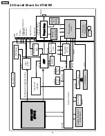
Page 96: ...5200 IC5300 IC5400 JK2001 S Video Aux Composite Video Out PB PR Y Video Out Head Phone Music Port Video Buffer Tuner Pack FM AM Headphone Amp System Control Loading Mechanism Control Block EEPROM Display Driver FL Display Regulator DC Det Motor Drive Music Port Amp AC IN and Transformer Power supply control AC Speaker subwoofer Terminal For Speaker Power Amp Power Amp ASP SA HT441W XM Ready Select...

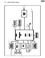
Page 97: ...C BEP MPEG2 Decode SP Motor TRV Motor IC8611 TRV sw CD DVD IC8251 IC8151 2 7V to 1 2V IC8001 IC8051 IC8421 IC8651 Driver FO TR Act TRV SP Motor DC DC Converter IC8111 5V to 3 3V OPU DC DC Converter LD Drive LD Drive EEPROM M M SD RAM SD RAM Flash ROM Flash ROM Audio DAC From Main Power Circuit SA HT441WP 97 ...

Page 98: ...T In TUNER In DVD Module ON ON DVD Mix L R DVD Front L R Volume DVD Center DVD Sub Woofer DVD Surround L R AGC ASS IC2103 DVD 5 1ch Play Back Mode IC2102 IC2906 IC2105 H P Amp Head Phone Front L R Center Sub Woofer Surround L R IC5000 IC5200 IC5300 IC5400 HIC ASP SA HT441WP 98 ...

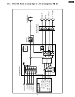
Page 99: ...TCR In AUX In TUNER In DVD Module HDMI ON DVD Mix L R DVD Front L R Volume DVD Center DVD Sub Woofer DVD Surround L R AGC ASS IC2103 2ch Analog input Mode IC2102 H P Amp Head Phone ASP Front L R Center Sub Woofer Surround L R HIC IC5000 IC5200 IC5300 IC5400 SA HT441WP 99 ...

Page 100: ...IVE Q2906 Q2907 Q2903 D2902 30V VCC 30V F F VP 12V 7V REG IC2903 IC2908 IC2907 IC2902 IC2901 Q2935 D2912 Q2904 D2915 D2934 SYS 6V IC2003 IC2904 FOR WIRELESS MODELS ONLY DVD MODULE IC2102 C 9V C 9V RF 5V IC2103 REG VCC T 9V C 9V MUTING DVD PCONT HIC SECTION POWER IC5000 IC5200 IC5300 IC5400 SW 5V DAMP 5V 13V M 9V TUNER FL DISPALY MAIN POWER ON MODE AC INPUT ON SA HT441WP 100 ...

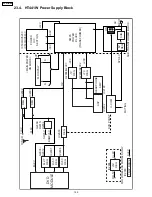
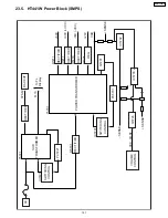
Page 101: ...02 IC5703 Q5726 RECTIFIER RECTIFIER RECTIFIER RECTIFIER BACKUP T5701 T5721 D5711 D5717 50V 30V VCC 30V VCC 20V SENSE SENSE VCC_CONT SENSE VDD D5716 D5701 IC5701 IC5721 D5705 SYS6V To FL Display F F RECTIFIER SWITCHING CONTROL PC5721 AC POWER TRANSFORMER SUB TRANSFORMER SA HT441WP 101 ...

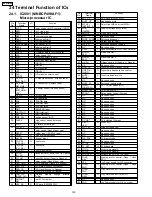
Page 102: ...direction Tx Rx 47 RMPORT_ DET I Rear M Port detect 48 ASP_DA O ASP data R2S15203FP Pin No Terminal Name I O Function 49 ASP_CK O ASP clock R2S15203FP 50 MUTE_HP O Headphone mute 51 MP_SEL SELECT_ A O Select front MPort or rear MPort 52 SUB_ LIMITER O Subwoofer frequency Limiter 53 VMUTE O Video mute control 54 N C No connection 55 WIDE_ SURR O Surround Enhancer 56 CEC_OUT I Output port for HDMI 5...

Page 103: ...25 Explode Views 25 1 Cabinet Parts Location 103 SA HT441WP ...

Page 104: ...104 SA HT441WP ...

Page 105: ...105 SA HT441WP ...

Page 106: ...25 2 Packaging 106 SA HT441WP ...

Page 107: ...acity values are in microfarads µF unless specified otherwise P Pico farads pF F Farads F Resistance values are in ohms unless specified otherwise 1K 1 000 OHM 1M 1 000K OHM The parenthesized indications in the Remarks columns specify the model names and areas Refer to the cover page The marking RTL indicates the retention time is limited for this item After the discontinuation of this assembly in...

Page 108: ...X0206 PC SHEET COVER B M 64 RMVX0096 XM COVER M 65 RXXX0084 HEATSINK UNIT M 66 RSCX0145 XM ANGLE M TRAVERSE DECK 301 RDG0567 PULSE GEAR M 302 RDG0568 OPEN LOCK GEAR M 303 RDG0569 1 CLOSE LOCK GEAR M Ref No Part No Part Name Description Remarks 304 RDV0073 TRAY BELT M 305 REZ1734 FFC WIRE M 306 RGQ0446 K TRAY BASE M 307 RGQ0359 K1 ROTARY TRAY M 308 RMM0254 2 SLIDE PLATE R M 309 RMB0842 TRAY SPRING ...

Page 109: ...ANSISTOR M Q2907 B1ADCF000001 TRANSISTOR M Q2909 B1GBCFJN0033 TRANSISTOR M Q2911 B1ABCF000176 TRANSISTOR M Q2912 B1ABCF000176 TRANSISTOR M Q2913 B1ABCF000176 TRANSISTOR M Q2914 B1ADCF000001 TRANSISTOR M Q2935 B1BACD000018 TRANSISTOR M Q2936 B1GBCFJN0033 TRANSISTOR M Q5101 B1ABCF000176 TRANSISTOR M Ref No Part No Part Name Description Remarks Q5102 B1ABCF000176 TRANSISTOR M Q5500 B1ADCE000012 TRANS...

Page 110: ...HC0000045 CHIP INDUCTOR M LB8503 ERJ2GE0R00X CHIP RESISTOR M LB8504 J0JCC0000119 CHIP INDUCTOR M LB8505 J0JCC0000119 CHIP INDUCTOR M Ref No Part No Part Name Description Remarks LB8507 J0JCC0000119 CHIP INDUCTOR M LB8511 ERJ3GEY0R00V CHIP RESISTOR M LB8512 ERJ3GEY0R00V CHIP RESISTOR M LB8513 ERJ3GEY0R00V CHIP RESISTOR M LB8514 ERJ3GEY0R00V CHIP RESISTOR M LB8690 J0JCC0000091 FILTER M LB8691 ERJ2GE...

Page 111: ...04 J0JBC0000019 CHIP INDUCTOR M L6905 J0JBC0000019 CHIP INDUCTOR M L8201 G1C100K00020 CHIP INDUCTOR M L8202 J0JCC0000079 FILTER M L8301 G1C100KA0055 CHIP INDUCTOR M L8302 J0JCC0000079 FILTER M L8550 G1C100KA0055 CHIP INDUCTOR M T5701 ETS42BJ1G4AC TRANSFORMER MAIN M T5721 ETS19AB1Z6AG TRANSFORMER SUB M COMPONENT COMBINATION Z6900 B3MAZ0000023 REMOTE CONTROL SENSOR M FUSE HOLDERS ZA5701 EYF52BCY FUS...

Page 112: ...16W M R2033 ERJ3GEYJ102V 1K 1 16W M Ref No Part No Part Name Description Remarks R2034 ERJ3GEYJ221V 220 1 16W M R2036 ERJ3GEYJ221V 220 1 16W M R2037 ERJ3GEYJ221V 220 1 16W M R2038 ERJ3GEYJ221V 220 1 16W M R2039 ERJ3GEYJ223V 22K 1 16W M R2040 ERJ3GEYJ223V 22K 1 16W M R2041 ERJ3GEYJ223V 22K 1 16W M R2042 ERJ3GEYJ472V 4 7K 1 16W M R2043 ERJ3GEYJ104V 100K 1 16W M R2044 ERJ3GEYJ221V 220 1 16W M R2045 E...

Page 113: ...222V 2 2K 1 16W M R2500 ERJ3GEYJ123V 12K 1 16W M R2501 ERJ3GEYJ273V 27K 1 16W M R2502 ERJ3GEYJ203V 20K 1 16W M Ref No Part No Part Name Description Remarks R2503 ERJ3GEYJ472V 4 7K 1 16W M R2510 ERJ3GEYJ123V 12K 1 16W M R2511 ERJ3GEYJ123V 12K 1 16W M R2512 ERJ3GEYJ103V 10K 1 16W M R2513 ERJ3GEYJ222V 2 2K 1 16W M R2600 ERJ3GEYJ123V 12K 1 16W M R2601 ERJ3GEYJ153V 15K 1 16W M R2606 ERJ3GEYJ563V 56K 1 ...

Page 114: ... ERJ1TYJ220U 22 1W M R5302 ERJ8GEYJ100V 10 1 8W M R5305 ERJ8GEYJ100V 10 1 8W M R5306 ERJ3GEYJ562V 5 6K 1 16W M Ref No Part No Part Name Description Remarks R5307 ERJ3GEYJ562V 5 6K 1 16W M R5310 ERJ8GEYJ100V 10 1 8W M R5311 ERJ8GEYJ100V 10 1 8W M R5318 ERJ3GEYJ124V 120K 1 16W M R5319 ERJ1TYJ220U 22 1W M R5328 ERJ3GEYJ124V 120K 1 16W M R5400 ERJ1TYJ220U 22 1W M R5402 ERJ8GEYJ100V 10 1 8W M R5405 ERJ...

Page 115: ... ERJ2GEJ153X 15K 2W M R8235 ERJ2GEJ822X 8 2K 2W M R8236 ERJ2GEJ822X 8 2K 2W M R8241 ERJ2GEJ223X 22K 2W M R8242 ERJ2GEJ752X 7 5K 2W M Ref No Part No Part Name Description Remarks R8243 ERJ2GEJ103X 10K 2W M R8251 ERJ6GEYJ6R8V 6 8 1 10W M R8261 ERJ2GEJ823X 82K 2W M R8262 ERJ2GEJ472X 4 7K 2W M R8263 ERJ2GEJ823X 82K 2W M R8264 ERJ2GEJ472X 4 7K 2W M R8265 ERJ2GE0R00X 0 2W M R8311 ERJ2RHD242X 2 4K 2W M R...

Page 116: ... M W2264 ERJ3GEY0R00V CHIP RESISTOR M W2265 ERJ6GEY0R00V CHIP RESISTOR M W2266 ERJ6GEY0R00V CHIP RESISTOR M W2267 ERJ3GEY0R00V CHIP RESISTOR M W2268 ERJ6GEY0R00V CHIP RESISTOR M W2270 ERJ6GEY0R00V CHIP RESISTOR M Ref No Part No Part Name Description Remarks W2272 ERJ6GEY0R00V CHIP RESISTOR M W2273 ERJ6GEY0R00V CHIP RESISTOR M W2274 ERJ6GEY0R00V CHIP RESISTOR M W2301 G0C220JA0055 COIL M W5201 ERJ3G...

Page 117: ...471K 470P 50V M C2214 ECJ1VB1H562K 5600P 50V M C2215 ECJ1VC1H181J 180P 50V M Ref No Part No Part Name Description Remarks C2217 ECJ1VB1C104K 0 1 16V M C2218 ECJ1VB1C104K 0 1 16V M C2219 ECJ1VB1A105K 1 10V M C2220 ECJ1VB1C333K 0 033 16V M C2221 ECJ1VB1C683K 0 068 16V M C2222 ECJ1VC1H100D 10P 50V M C2260 ECJ1VC1H181K 180P 50V M C2261 ECJ1VB1C393K 0 039 16V M C2262 ECJ1VC1H101K 100P 50V M C2264 ECJ1V...

Page 118: ...CJ1VB1H103K 0 01 50V M C2957 ECJ1VB1H103K 0 01 50V M C2958 ECJ1VB1H103K 0 01 50V M Ref No Part No Part Name Description Remarks C2960 ECJ1VB1A105K 1 10V M C2962 ECEA1CKA101B 100 16V M C2963 EEUFC1C471B 470P 16V M C2964 ECJ1VB1H103K 0 01 50V M C2965 ECJ1VB1H103K 0 01 50V M C2966 ECJ1VB1H103K 0 01 50V M C2967 ECJ1VB1H103K 0 01 50V M C2968 ECEA1CKA101B 100 16V M C2969 ECEA1CKA101B 100 16V M C2970 EEU...

Page 119: ...0V M C5409 ECJ3YB2A104K 0 1 100V M C5410 ECJ3YB2A104K 0 1 100V M C5411 ECJ2VC2A221J 220P 100V M C5412 ECJ1VB1H331K 330P 50V M Ref No Part No Part Name Description Remarks C5413 ECJ1VB1H104K 0 1 50V M C5416 ECJ1VB1H104K 0 1 50V M C5418 ECJ3YB2A104K 0 1 100V M C5419 ECJ3YB2A104K 0 1 100V M C5420 ECJ3YB2A104K 0 1 100V M C5421 ECJ1VB1C224K 0 22 16V M C5422 ECJ1VB1H153K 0 015 50V M C5423 ECJ1VC1H221J 2...

Page 120: ... 1 6 3V M C8052 ECJ0EF1C104Z 0 1 16V M C8053 ECJ0EC1H221J 220P 50V M C8054 ECJ1VB0J105K 1 6 3V M Ref No Part No Part Name Description Remarks C8055 ECJ1VB0J105K 1 6 3V M C8056 ECJ0EF1C104Z 0 1 16V M C8057 ECJ0EB1E222K 2200P 25V M C8111 ECJ0EB1A104K 0 1 10V M C8112 ECJ1VB0J105K 1 6 3V M C8113 ECJ0EB1E471K 470P 25V M C8151 ECJ2YB0J225K 2 2 6 3V M C8152 ECJ1VB1C105K 1 16V M C8201 F2H0J101A003 100 6 3...

Page 121: ...8562 F2G1C100A072 10 16V M C8563 F2H0J470A003 47 6 3V M C8564 ECJ1VB0J105K 1 6 3V M C8601 ECJ0EF1C104Z 0 1 16V M C8606 ECJ0EF1C104Z 0 1 16V M C8607 ECJ0EB0J224K 0 22 6 3V M C8611 ECJ0EF1C104Z 0 1 16V M C8621 ECJ0EC1H120J 12P 50V M C8622 ECJ0EC1H120J 12P 50V M C8651 ECJ0EF1C104Z 0 1 16V M C8652 ECJ0EF1C104Z 0 1 16V M C8691 ECJ0EF1C104Z 0 1 16V M C8695 ECJ0EF1C104Z 0 1 16V M 121 SA HT441WP ...

Reviews: