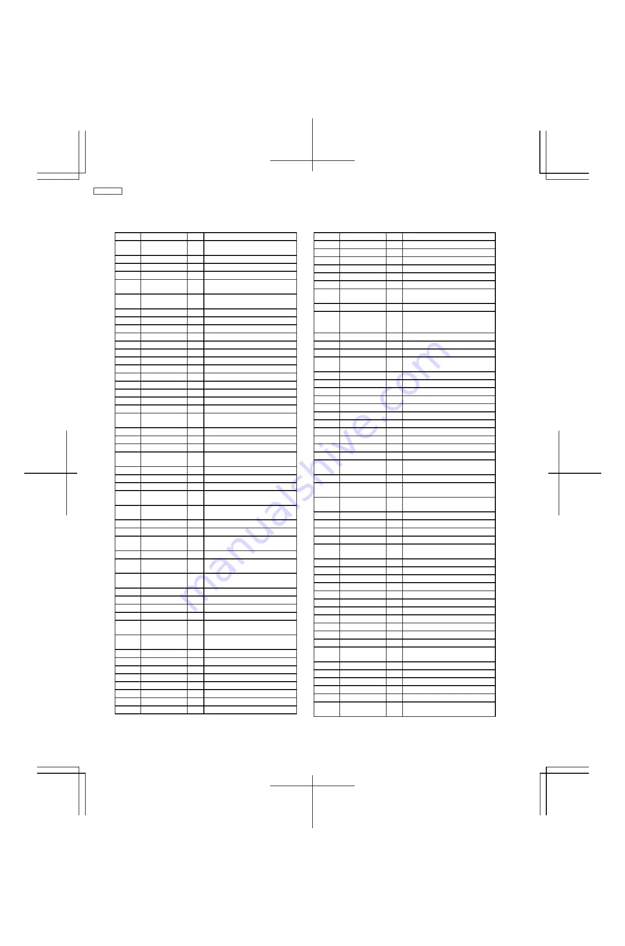
Pin No.
Mark
I/O
Function
1
EEPR_DATA
OUT
-
NO CONNECTION
2
EEPR_DATA IN
-
NO CONNECTION
3
EEPR_CLK
-
NO CONNECTION
4
CD_MDATA
O
CD MICRO-P DATA
5
CD_STAT
I
553 LSI ( CD_SUBQ combine
CD_STAT)
6
CD_MCLK
O
553 LSI (CD_SQCK combine with
CD_MCLK)
7
HALT
I
AC DETECTION INPUT
8
OCD_SDA
I/O
OCD SERIAL DATA INPUT
9
OCD_SCL
I/O
OCD SERIAL CLOCK OUTPUT
10
CRTIMER
I/O
CR TIMER
11
MMOD
I
USB NORMAL/WRITE MODE
12
XTOUT
O
OSCILLATOR OUTPUT
13
XTIN
I
OSCILLATOR INPUT
14
VSS
-
GND
15
XTIN1
I
OSCILLATOR INPUT
16
XTOUT1
O
OSCILLATOR OUTPUT
17
VDD33
-
VOLTAGE 3.3V
18
VDD18
-
VOLTAGE 1.8V
19
MICOMRST
I
MICRO-PROCESSOR RESET
20
LON
I
Using Internal Regulator, Connect
to H.
21
D_MPUCLK
-
NO CONNECTION
22
D_MPURX
-
NO CONNECTION
23
D_MPUTX
-
NO CONNECTION
24
OCDMOD
I
Using Internal Regulator, Connect
to H.
25
REST SW
I
RESET SWITCH
26
RMT
I
REMOTE CONTROL INPUT
27
D_DDOWFIC
-
EDGE DETECTOR
28
CD_BLKCK
I
CD SUBCODE BLOCK CLOCK
INPUT
29
POWERDET
I
POWER DETECT INPUT
SIGNAL
30
PCONT
O
POWER CONTROL OUTPUT
31
NC
-
NO CONNECTION
32
CD_RST
O
CD LSI RESET OUTPUT (L:
RESET)
33
CD_MLD
O
CD LSI COMMAND LOAD
34
SD_CMD
(RXDIN)
O
DATA OUTPUT TO SD MODULE
35
SD_STATUS
(TXDOUT)
I
DATA INPUT TO SD MODULE
36
SD_NRST
O
DAB DECODER LSI RESET
37
VDD18
-
VOLTAGE 1.8V
38
DOCK_PLAY
O
DOCK PLAY CONTROL SIGNAL
39
VSS
-
GND
40
DOCK_RSKIP
O
DOCK REVERSE SKIP
CONTROL
41
DOCK_FSKIP
O
DOCK FORWARD SKIP
CONTROL
42
DOCK_ PAUSE
O
DOCK PAUSE CONTROL
43
NC
-
NO CONNECTION
44
NC
-
NO CONNECTION
45
NC
-
NO CONNECTION
46
NC
-
NO CONNECTION
47
NC
-
NO CONNECTION
48
D_MPUMOD
-
NO CONNECTION
49
NC
-
NO CONNECTION
Pin No.
Mark
I/O
Function
50
CD_OPEN_ SW
I
CD OPEN SWITCH DETECTION
51
CLOSE_L
O
CD TRAY CLOSE
52
OPEN_H
O
CD TRAY OPEN
53
D_PLLSDA
-
NO CONNECTION
54
D_PLLSCL
-
NO CONNECTION
55
MUTE_A
O
HP/SP MUTING CONTROL
56
ASP_CLK
O
ASP CONTROL (CLOCK
SIGNAL)
57
ASP_DATA
O
ASP CONTROL (DATA SIGNAL)
58
DEMO
I
AUTO DEMO INITIAL SETTING,
(L: ON, H: OFF) DEFAULT:
On(L)
59
D_TURST
-
NO CONNECTION
60
D_NRFRESET
-
NO CONNECTION
61
VDD33
-
VOLTAGE 3.3V
62
HP_SW
I
MUTING CONTROL FOR
HEADPHONE ON/OFF
63
VSS
-
GND
64
EEPR_ HOLDB
-
NO CONNECTION
65
EEPR_CS
-
NO CONNECTION
66
EEPR_WP
-
NO CONNECTION
67
D_PON
-
NO CONNECTION
68
SD_INT
O
SD INT OUTPUT
69
RDS_ID
-
NO CONNECTION
70
DPRT_DET1
I
DPORT DETECT 1 INPUT
71
DPRT_DET2
I
DPORT DETECT 2 INPUT
72
RDS_DATA
-
NO CONNECTION
73
RDS_CLK
-
NO CONNECTION
74
FHOP1
O
FREQUENCY SHITFING FOR
DIGITAL AMP
75
VDD18
-
VOLTAGE 1.8V
76
DPRT_RXD
(UART_OUT)
O
D-PORT UART DATA OUTPUT
77
DPRT_TXD
(UART_IN)
I
D-PORT UART DATA INPUT
78
IPOD_DET
I
IPOD DETECT INPUT
79
TU_SDA
O
TUNER SERIAL DATA INPUT
80
TU_STEREO
I
TUNER STEREO SIGNAL
81
NC
-
NO CONNECTION
82
MUTE_F
O
MUTING CONTROL FOR
FRONT
83
AMP_MODE
O
D-AMP MODE SIGNAL
84
TU_CLK
O
TUNER CLOCK SIGNAL
85
TU_TUNED
O
TUNER TUNED SIGNAL
86
AUX_DET
I
AUX DETECT INPUT
87
DPRT_ PCONT
O
5V SUPPLY PIN
88
DCDET
I
POWER DETECTION INPUT
89
VDD5
-
VOLTAGE 5V
90
NC
-
LED CONTROL
91
VSS
-
GND
92
FAN_IN2
-
NO CONNECTION
93
REGION
I
TUNER REGION SETTING
94
POWERDET /
FAN_IN
-
NO CONNECTION
95
KEY1
I
KEY INPUT 1
96
KEY2
I
KEY INPUT 2
97
VOL_JOG
I/O VOLUME JOG
98
TRE_JOG
I/O TREBLE JOG
99
BASS_JOG
I/O BASS LEVEL CONTROL
100
VHREF
-
CONNECT EXTERNAL
RESISTOR TO VDD5
19 Terminal Function of IC’s
19.1. IC2801 (RFKWPMX3GN) IC MICROPROCESSOR
88
SA-PMX3GN
Summary of Contents for SA-PMX3GN
Page 10: ...6 Operation Procedures 6 1 Main Unit Key Buttons Operation 10 SA PMX3GN ...
Page 11: ...6 2 Remote Control Key Buttons Operation 6 3 Disc Information 11 SA PMX3GN ...
Page 18: ...18 SA PMX3GN ...
Page 20: ...8 2 Main Parts Location Diagram 20 SA PMX3GN ...
Page 56: ...56 SA PMX3GN ...
Page 58: ...SA PMX3GN 58 ...
Page 64: ...SA PMX3GN 64 ...
Page 66: ...66 SA PMX3GN ...
Page 86: ...SA PMX3GN 86 ...
Page 91: ...20 Exploded Views 20 1 Cabinet Parts Location SA PMX3GN 91 ...
Page 92: ...20 2 Packaging SA PMX3GN 92 ...