background image

O

O

O

O

GENERAL

Power Supply:

AC 120 V, 60 Hz

Power Consumption:

131 W

Dimensions (W×H×D):

430×75×424 mm

Mass:

Main unit 5 kg

Operating Temperature Range:

+5°C to +35°C

Operating Humidity Range:

5% to 90% RH (no
condensation)

O

O

O

O

AMPLIFIER SECTION

RMS Output Power: Dolby Digital Mode

O

O

O

O

Total RMS Dolby Digital mode power:

1000 W

At 1 kHz and total harmonic of 10%

O

O

O

O

Front Ch:

125 W / Channel (3

)

O

O

O

O

Center Ch:

250 W / Channel (6

)

O

O

O

O

Surround Ch:

125 W / Channel (3

)

At 100 Hz and total harmonic of 10%

O

O

O

O

Subwoofer Ch:

250 W / Channel (6

)

FTC Output Power: Dolby Digital Mode

O

O

O

O

Total FTC Dolby Digital mode power:

428 W

At 120 Hz - 20 kHz and total harmonic of 1%

O

O

O

O

Front Ch:

63 W / Channel (3

)

O

O

O

O

Center Ch:

113 W / Channel (6

)

O

O

O

O

Surround Ch:

34 W / Channel (3

)

© 2007 Matsushita Electric Industrial Co., Ltd. All
rights

reserved.

Unauthorized

copying

and

distribution is a violation of law.

SA-PT750PL

Colour

(K).......................Black Type

At 45 Hz - 120 Hz and total harmonic of 1%

O

O

O

O

Subwoofer Ch:

121 W / Channel (6

)

O

O

O

O

FM/AM TUNER, TERMINALS SECTION

Preset Memory:

FM 30 stations
AM / MW 30 stations

Frequency Modulation (FM)

Frequency range:

87.9-107.9 MHz

(200-kHz step)

87.5-108.0 MHz

(100-kHz step)

Sensitivity:

1.8 µV (IHF)

S/N 26 dB:

1.4 µV

Antenna terminals:

75

(unbalanced)

Amplitude Modulation (AM/MW):

Frequency range:

520-1710 kHz (10-kHz step)

AM Sensitivity S/N 20 dB at
1000 kHz:

560 µV/m

Phone Jack:

Terminal:

Stereo, 3.5 mm jack

Music Port (Front):

Sensitivity:

100 mV, 1.2 k

Terminal (Input):

Stereo, 3.5 mm jack

O

O

O

O

DISC SECTION

Discs played [8 cm or 12 cm]:

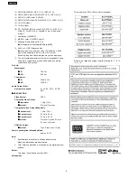
(1) DVD (DVD-Video)

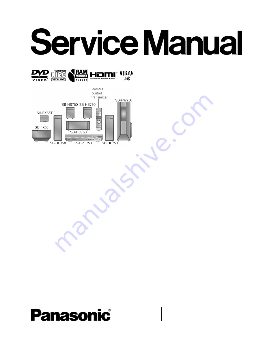
DVD Home Theater Sound System

Specifications

ORDER NO. MD0706006CE

Summary of Contents for SA-PT750PL

Page 1: ...ter Ch 113 W Channel 6Ω O O O OSurround Ch 34 W Channel 3Ω 2007 Matsushita Electric Industrial Co Ltd All rights reserved Unauthorized copying and distribution is a violation of law SA PT750PL Colour K Black Type At 45 Hz 120 Hz and total harmonic of 1 O O O OSubwoofer Ch 121 W Channel 6Ω O O O OFM AM TUNER TERMINALS SECTION Preset Memory FM 30 stations AM MW 30 stations Frequency Modulation FM Fr...

Page 2: ...ick Up Wavelength O O O OCD 785 nm O O O ODVD 662 nm Laser power O O O OCD CLASS 1M O O O ODVD CLASS 1 Audio Output Disc Number of channels 5 1 ch FL FR C SL SR SW O O O OVIDEO SECTION Video System NTSC Composite Video Output O O O OOutput level 1 Vp p 75 Ω O O O OTerminal Pin jack 1 system Component Video Output 480p 480i O O O OY output level 1 Vp p 75 Ω O O O OPB output level 0 7 Vp p 75 Ω O O ...

Page 3: ...less Adapter P C B 54 10 11 Disassembly of Tray P C B 54 10 12 Disassembly of D Amp P C B 55 10 13 Disassembly of Digital Amp IC IC5000 55 10 14 Disassembly of DVD Module P C B 56 10 15 Disassembly of Main P C B 56 10 16 Disassembly of Regulator IC IC2903 57 10 17 Disassembly of SMPS AC Inlet P C B 58 10 18 Disassembly of Switch Regulator IC IC5701 58 10 19 Disassembly of Regulator Diode D5803 59 ...

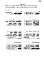
Page 4: ...t Circuit 111 21 Printed Circuit Board 113 21 1 DVD Module P C B 113 21 2 Main P C B 114 21 3 Panel Key Wireless Adapter P C B 115 21 4 D Amp P C B 116 21 5 SMPS P C B 117 21 6 AC Inlet Tray Loading Motor Tray Motor Sensor P C B 118 22 Basic Troubleshooting Guide 119 22 1 Basic Troubleshooting Guide for Traverse Unit DVD Module P C B 119 22 2 Basic Troubleshooting Guide for HDMI AV output 120 23 O...

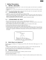
Page 5: ...ure 1 3 Use an AC voltmeter with 1000 ohms volt or more sensitivity to measure the potential across the resistor 4 Check each exposed metallic part and measure the voltage at each point 5 Reverse the AC plug in the AC outlet and repeat each of the above measurements 6 The potential at any point should not exceed 0 75 volts RMS A leakage current tester Simpson Model 229 or equivalent may be used to...

Page 6: ... PC5701 B3PBA0000402 PHOTO COUPLER M PC5702 B3PBA0000402 PHOTO COUPLER M PC5720 B3PBA0000402 PHOTO COUPLER M PC5799 B3PBA0000402 PHOTO COUPLER M D5701 B0FBAR000041 DIODE M DZ5701 ERZV10V511CS ZENER M TH5701 D4CAA5R10001 THERMISTOR M TH5860 D4CC11040013 THERMISTOR M L2101 J0JBC0000015 CHIP INDUCTOR M L2201 J0JBC0000015 CHIP INDUCTOR M L2802 J0JBC0000015 CHIP INDUCTOR M L2803 J0JBC0000015 CHIP INDUC...

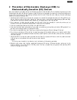
Page 7: ...bly 3 Use only a grounded tip soldering iron to solder or unsolder ES devices 4 Use only an anti static solder removal device Some solder removal devices not classified as anti static ESD protected can generate electrical charge sufficient to damage ES devices 5 Do not use freon propelled chemicals These can generate electrical charges sufficient to damage ES devices 6 Do not remove a replacement ...

Page 8: ... power from pickup 100µW VDE Laser radiation from pickup unit is safety level but be sure the followings 1 Do not disassemble the pickup unit since radiation from exposed laser diode is dangerous 2 Do not adjust the variable resistor on the pickup unit It was already adjusted 3 Do not look at the focus lens using optical instruments 4 Recommend not to look at pickup lens for a long time 8 SA PT750...

Page 9: ...ork using Lead Free Solder PbF The lead free solder has to be used when repairing the equipment for which the lead free solder is used Definition The letter of PbF is printed on the PCB using the lead free solder To put lead free solder it should be well molten and mixed with the original lead free solder Remove the remaining lead free solder on the PCB cleanly for soldering of the new IC Since th...

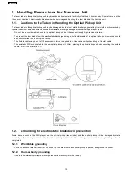
Page 10: ... flexible cable of the optical pickup unit removed should be short circuited with a short pin or a clip 3 The flexible cable may be cut off if an excessive force is applied to it Use caution when handling the flexible cable 4 The antistatic FPC is connected to the new optical pickup unit After replacing the optical pickup unit and connecting the flexible cable cut off the antistatic FPC 5 2 Ground...

Page 11: ...11 SA PT750PL ...

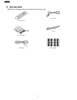
Page 12: ...Remote control AM loop antenna Antenna wire Video Cable AC cord Speaker label 6 Accessories Note Refer to Replacement Parts List Section 26 for the part number 12 SA PT750PL ...

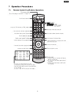
Page 13: ...nd play a disc automatically Show a disc menu or play list Select the disc or show disc information Display current playback condition Select preset radio stations channels Television operations Select the source DVD DVD CD TUNER BAND FM AM SELECT SELECT DVD CD FM AM AUX MUSIC P Mute the sound MUTING flashes in the main unit s display while the function is on To cancel press the button again or ad...

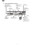
Page 14: ...olume of the main unit TUNING Headphone plug type 3 5 mm stereo mini plug Reduce the volume before connecting Audio is automatically switched to 2 channel stereo To prevent hearing damage avoid listening for prolonged periods of time OPEN CLOSE Open Close the disc drawer TUNE MODE FM MODE Stop playing Select the tuning mode Adjust the FM reception condition Play discs Memorize the receivng i radio...

Page 15: ...cator lights red when the wireless system is turned on and lights green when the wireless link is activated When the wireless link is inactive for a long time it turns red Use this button to turn the wireless system on and off The unit is on The unit is off 7 3 2 Digital Transmitter Connection SH FX65T 15 SA PT750PL ...

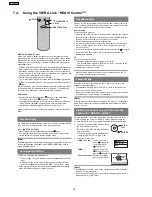
Page 16: ...ls refer to the operating instructions of your television Home Cinema Theater speakers are active When the home theater system is in standby mode changing the television speakers to theater speakers in the television menu will automatically turn the home theater system on and select AUX as the source The television speakers are automatically muted You can control the volume setting using the volum...

Page 17: ...7 5 Using the Music Port 28 17 SA PT750PL ...

Page 18: ...scs VCD Music discs with video Including SVCD Conforming to IEC62107 CD CD Music discs Logo Recorded on a DVD video recorder etc Recorded on a personal computer etc DVD VR 2 WMA MP3 JPEG Not Necessary Necessary DVD R DL Necessary R RW Necessary Necessary Commercial discs Video CD Recorded discs Playable Not playable DVD V 4 6 Finalizing 3 5 5 Necessary 7 1 R DL DVD R RW DVD RAM Disc CD R RW Refer ...

Page 19: ...d This unit does not support Multiple Bit Rate MBR an encoding process for audio content that produces an audio file encoded at several different bit rates MP3 DVD RAM DVD R RW CD R RW MP3 mp3 Compatible compression rate between 32 kbps and 320 kbps for sampling frequencies of 32 kHz and above between 8 kbps and 160 kbps for sampling frequencies of 24 kHz and below This unit does not support ID3 t...

Page 20: ...8 New Features 8 1 About HDMI 8 1 1 What is HDMI 8 1 2 Advanced Digital Pictures 20 SA PT750PL ...

Page 21: ...8 1 3 Advanced Digital Sound 8 1 4 Easy to Use 8 1 5 HDMI Compatible Products 21 SA PT750PL ...

Page 22: ...audio received by the FX65 FX66 receiver Maximum range attainable is 30 meters 8 2 1 3 FX85 The FX85 supports the multi room function wherein it operates as a second room wireless receiver up to a maximum of two Maximum range attainable is 30 meters It can send commands to the main unit to control functions such as Play Stop Forward Skip Channel Up Reverse Skip Channel Down It also has a built in ...

Page 23: ...M CH2 IN DAC BB RF EEPROM CH2 OUT Note One way only FX65 FX66 signal flow FX65 FX66 only TX Type A RX Type 1 MCU Type A transmitter uses one ADC Analog to Digital Converter and transmits audio through Channel 2 Type 1 receiver Rx uses one DAC and output audio through Channel 2 The firmware that is downloaded to EEPROM IC multiplexes which channel to listen to in this case Channel 2 since type A is...

Page 24: ... Surround Music DPL or Super Surround Music Movie FX85 Wireless feature is enabled by default when the user uses transmitter type B 8 2 4 LED Indication For FX65 FX66 there will be two color LED that will be used to indicate Power On and Link If link the two color LED will be green else it will be red For FX85 the front panel will have LED indicators for Standby Wireless Link Charge Option and Mus...

Page 25: ... and three 3 key in the remocon Once ID setting is triggered the receiver must press its ID setting button within 60 seconds During this period the transmitter will be in open connect mechanism whereby any receiver can pair with the transmitter After this period elapsed the transmitter will revert back to using close connect code whereby only those receivers which have the same ID as the transmitt...

Page 26: ... to the main set such as Play Stop Skip and Preset Tuner Channel Up Down This configuration uses Type B transmitter which is an upgrade of the Type A and can be used on Type 1 FX65 FX66 This transmitter is able to send audio signal for second room via Ch 1 and first room via Ch 2 In this configuration streams AB is used to transmit the audio from main unit to the first room Type 1 receiver FX65 FX...

Page 27: ... receiver FX65 FX66 through streams AB via Ch 2 and Type 2 second room receiver FX85 comes from transmitter B through streams CD via Ch 1 For this configuration the user must perform ID setting for FX85 if it is sold as an accessory but for bundled type it already is paired with the transmitter RX RX RX RX CH2 AB CH2 AB CH1 CD B 1 1 1 Multi room Multi source 27 SA PT750PL ...

Page 28: ...selected baseband IC settings Not all baseband register settings a total of 512 bytes will be read from the EEPROM IC though Aside from getting the baseband settings from the EEPROM IC it is also used to enable FCC testing select the application type and entering into doctor mode this can be enabled also by sending a command via the main unit 8 2 9 Doctor Mode For normal operation but automatic fr...

Page 29: ...ommunication error display TOP MENU ECC error check EQ CPPM CRM keys check ENTER DVD Module P C B reset Timer 1 check Refer to the section 9 2 5 Service Mode Table 5 for more information Timer 1 reset Timer 2 check Timer 2 reset STOP 1 Combination reliability test mode Refer to the section 9 2 7 1 Test Mode List for more information 2 OPEN CLOSE reliability test mode 3 Tray rotation reliability te...

Page 30: ...hown in hexadecimal notation Display 1 Display 1 Display 2 Display 2 In STOP no disc mode press STOP button on the main unit and 0 button on the remote control unit With pointing of cursor up and down on display Error code check The latest error code stored in the EEPROM IC is displayed Note Refer to Section 9 5 DVD Self Diagnostic Function Error Code for more detailed information on the error cod...

Page 31: ...OP button on the main unit and 1 button on the remote ADSC internal RAM data check ADSC internal RAM data is read out and displayed The value is shown in hexadecimal notation The above example shows the data in ADSC address FBOh is XXXXh Address RAM data for specified address DVD laser drive current measurement Press FL Display on remote control unit for next page FL Display on values of dvd drive...

Page 32: ...main unit and 10 button on the remote control unit If the EEPROM version matches checksum YYYY is displayed If the version of the EEPROM does not match NG is displayed a If there is NO EEPROM header string OR b If there is no EEPROM no data is received by Micro processor NO is displayed EEPROM Checksum If applicable refer below Condition1 Opecon Version Display 1 Display 2 Display 3 Condition 2 Co...

Page 33: ...n GK China 6 PAL NTSC B 6PN English Simplified Chinese 5P6 PAL C SECAM 5 NTSC 4 4 GN EE CIS PL GCP LB 3PN 4P6 PAL C PAL 2P6 PAL C PAL 2 2P6 PAL C PAL 2 1PN NTSC 1 E Europe 2 PAL PAL C 2P6 P PC PX USA Canada PX NTSC A Europe GC GS EB EG Middle East 3 NTSC B Product OSD Menu Language Model Series Country Region Region Explanation of Display Individual Model Code can play PAL disc Region code N If NT...

Page 34: ...it and EQ button on the remote control unit No of communication error No of communication ECC Lead Error Display 1 Display 2 Press POWER button to exit Press FL Display on remote control unit for next page FL Display Video Decode Error 0 NG 1 OK 0 NG 1 OK Audio Lead Error DVD Module P C B firmware version display Cancelled automatically 5 seconds later In STOP no disc mode press STOP button on the...

Page 35: ... for DVD laser and CD laser FL Display sequence Display 1 2 Press FL Display button for next page of FL Display Timer 1 reset Laser operation timer of both DVD laser and CD laser is reset all at once Timer 2 check Spindle motor operation timer Timer 2 reset Spindle motor operation timer Time is shown in 5 digits of decimal notation in a unit of 1 hour 00000 will follow 99999 Shown to the above is ...

Page 36: ... into the unit if it is 23 DVD 34 CD or less Value is 23 DVD 34 CD or less Value is more than 23 DVD 34 CD Use the tilt adjustment check function Note Press FL DISPLAY button on remote Note Press FL DISPLAY button on remote control unit for next page display control unit for next page display Replace with a new optical pickup if the present value is more than 23 DVD 34 CD Cause Damage due to stati...

Page 37: ...Tray CLOSE DOWN DISC4 TocRead DOWN Tray Turn The right direction 1 section DISC5 TocRead DOWN Tray Turn The right direction 2 section DISC2 TocRead DOWN Tray Turn The right direction 1 section DISC3 TocRead DOWN Tray Turn The opposite direction 2 section DISC1 From the beginning The operation of the RC1 mechanism is carried out for the tray rotation the TOC Below is the flow sequence In STOP mode ...

Page 38: ...play Mecha o operation The k kind o of e error FL D Display The OPEN error under clamp rise H01 0 The OPEN error under clamp down H01 1 The CLOSE error under clamp rise H01 2 OPEN CLOSE The CLOSE error under clamp down H01 3 UP error H01 4 UP DOWN DOWN error H01 5 Right rotation error H01 6 TURN Reverse rotation error H01 7 TOC READ TOC READ error H01 8 FOCUS Timeout error H01 9 The right rotation...

Page 39: ... buttons Remote control unit buttons Application Note FAST FORWARD 3 ID setting Refer to the section 9 4 1 Service Mode Table 1 for more information STOP only in AUX 4 RF channel 1 display Refer to the section 9 4 2 Service Mode Table 2 for more information 5 RF channel 2 display 6 RF channel 3 display 7 Auto RF channel display Note Main room refers to the location of the main unit 39 SA PT750PL ...

Page 40: ...play 2 Display 3 Main room is in CD DVD mode Press and hold FAST FORWARD button on the main unit and 3 button on the remote control unit To set the ID in the Tx Rx The system goes into Pairing Mode P will be displayed for 60 seconds to indicate it is in Pairing Mode During this condition the ID set button on the receiver unit can be pressed to pair the Tx Rx After 60 seconds the FL display will re...

Page 41: ...l channels 1 2 or 3 RF channel channels 1 2 or 3 After 2 seconds Display 1 Display 2 Display 3 After 2 seconds Main room is in AUX mode Main room is in AUX mode Main room is in AUX mode Main room is in AUX mode Press and hold STOP button on the main unit and 4 button on the remote control unit Press and hold STOP button on the main unit and 5 button on the remote control unit After 2 seconds Press...

Page 42: ...error DV5 LSI IC IC8001 error H07 Driver IC thermal The spindle motor is abnormal short Press STOP on shut down between brushes main unit for next error H15 Disc tray open The disc tray cannot be opened it Press STOP on detection switch closes spontaneously main unit for next error failure H16 Disc tray close The disc tray cannot be closed it Press STOP on detection switch opens spontaneously main...

Page 43: ...in unit for next error F893 FLASH ROM IC data Firmware error DV5 LSI IC IC8651 Press STOP on falsification error error main unit for next error F894 EEPROM IC When failing in the access to Press STOP on abnormality error EEPROM IC located in the DVD main unit for next error Module P C B IC8611 F895 Language area Firmware version agreement check for Press STOP on abnormal factory preset setting fai...

Page 44: ...ion s changing due to wound etc of DISC and to have done the reproduction transition F601 Irregular sector ID It tried to access the position that did Press STOP on was demanded not exist on DISC by the recording main unit for next error error etc of authoring F603 KEYDET cannot be The data for decoding copyright Press STOP on acquired by the protection CSS cannot be acquired main unit for next er...

Page 45: ... operability and playability to the substandard discs processing to optimize the drive The recovery disc has also firmware version up After version up recovery processing is executed automatically Part number of the recovery disc for version up will be noticed when it is supplied Updating firmware 1 Load the recovery disc on to the player and run it 2 Firmware version of the player is automaticall...

Page 46: ...6 Power on the unit It should be no problem If problem persist check on the DVD Module P C B or FLASH ROM IC 46 SA PT750PL ...

Page 47: ...nt are required Disassembly of Top Cabinet Disassembly of Tray Lid Assembly Disassembly of Front Panel Disassembly of Panel Key P C B Disassembly of Tray Base Assembly Disassembly of Mechanism Base Assembly Disassembly of Rear Panel Disassembly of Wireless Adapter P C B Disassembly of Tray P C B Disassembly of D Amp P C B Disassembly of Digital Amp IC IC5000 Disassembly of DVD Module P C B Disasse...

Page 48: ... Disassembly of Support Piece Change Lever Slide Plate L Slide Plate R Disassembly of Cam Gear Assembly of Tray Base Assembly 48 SA PT750PL ...

Page 49: ...hange Lever Slide Plate L Slide Plate R 10 32 Magnet Holder Washer Magnet Clamper 10 12 D Amp P C B 10 10 Wireless Adapter P C B 10 31 Drive Gear A Drive Gear B 10 30 Loading Motor P C B 10 21 Regulator Diode D5702 10 22 Tray Guide L Tray Guide R 10 23 Rotary Tray 10 24 Open Lock Gear 10 25 Close Lock Gear 10 26 Tray Motor P C B 10 27 Sensor P C B 10 7 Tray Base Assembly 10 20 Regulator Diode D580...

Page 50: ...10 2 Main Components and P C B Locations 50 SA PT750PL ...

Page 51: ...ion of the arrow Step 2 Release the claws at the bottom of the tray lid assembly Step 3 Remove the tray lid assembly in the direction of arrow Note You can push back the tray base assembly by keeping the open lock gear pressed in anti clockwise direction 10 5 Disassembly of Front Panel Follow Step 1 to Step 3 of Item 10 3 Follow Step 1 to Step 3 of Item 10 4 Step 1 Detach FFC cable from the connec...

Page 52: ... B Step 4 Remove 7 screws Step 5 Remove Panel P C B and Key P C B 10 7 Dissassembly of Tray Base Assembly Follow Step 1 to Step 3 of Item 10 3 Follow Step 1 to Step 3 of Item 10 4 Follow Step 1 to Step 4 of Item 10 5 Step 1 Keep the close lock gear pressed in clockwise direction and move the tray base assembly in the direction of the arrow until the end of it Note Make sure the open lock gear is k...

Page 53: ...base assembly Caution Take note of the screw type used During assembling use the correct screw type and at the correct location Step 2 Detach FFC cable from the connector CN2005 on Main P C B Step 3 Lift up the right side of the mechanism unit to detach FFC cables from the connectors FP8251 FP8531 on DVD Module P C B Step 4 Remove the mechanism base assembly Caution Do not use strong or excessive ...

Page 54: ... cable from the connector CN2003 on Main P C B Step 3 Remove 4 screws on rear panel Step 4 Release the tab in direction of the arrow Step 5 Remove the Wireless Adapter P C B 10 11 Disassembly of Tray P C B Follow Step 1 to Step 3 of Item 10 3 Follow Step 1 to Step 3 of Item 10 4 Follow Step 1 to Step 4 of Item 10 5 Follow Step 1 to Step 4 of Item 10 7 Disassembly of Tray Guide R Step 1 Remove 1 sc...

Page 55: ...p 5 Remove the wire clamp to detach FFC cable from the connector CN5501 on D Amp P C B Step 6 Remove 5 screws on the rear panel Step 7 Release the tab in the direction of the arrow Step 8 Remove D Amp P C B Caution Be careful of the Heatsink Unit A which has high temperature after prolonged use when removing D Amp P C B 10 13 Disassembly of Digital Amp IC IC5000 Follow Step 1 to Step 3 of Item 10 ...

Page 56: ... Step 4 of Item 10 5 Follow Step 1 to Step 4 of Item 10 7 Follow Step 1 to Step 4 of Item 10 8 Follow Step 1 to Step 8 of Item 10 12 Step 1 Remove 2 screws on DVD Module P C B Step 2 Remove the top FFC cover from Main P C B Step 3 Remove the mecha bracket Step 4 Detach FFC cable from the connectors CN2001 CN2010 on Main P C B Step 5 Remove DVD Module P C B Caution Do not use strong or excessive fo...

Page 57: ... 10 16 Disassembly of Regulator IC IC2903 Follow Step 1 to Step 3 of Item 10 3 Follow Step 1 to Step 3 of Item 10 4 Follow Step 1 to Step 4 of Item 10 5 Follow Step 1 to Step 4 of Item 10 7 Follow Step 1 to Step 4 of Item 10 8 Follow Step 1 to Step 7 of Item 10 15 Step 1 Desolder pins of the regulator IC IC2903 on the back side of Main P C B Step 2 Remove 1 screw Step 3 Remove the regulator IC IC2...

Page 58: ... SMPS P C B Step 4 Remove the P C B bracket Step 5 Remove 1 screw from the rear panel Step 6 Release the tab in the direction of arrow Step 7 Remove SMPS AC Inlet P C B Caution Be careful of power heatsinks located on D Amp P C B which has high temperature after prolonged use when removing it 10 18 Disassembly of Switch Regulator IC IC5701 Follow Step 1 to Step 3 of Item 10 3 Follow Step 1 to Step...

Page 59: ...p 7 of Item 10 17 Step 1 Desolder pins of the regulator D5803 on the back side of SMPS P C B Step 2 Remove 1 screw Step 3 Remove the diode D5803 from the heatsink unit C Caution Handle the heatsink unit C with caution due to its high temperature after prolonged use Touching it may lead to injuries Note Refer to the diagrams of SMPS P C B Item 10 18 for location of the parts 10 20 Disassembly of Re...

Page 60: ...7 Step 1 Desolder pins of the regulator diode D5702 on the back side of SMPS P C B Step 2 Remove 1 screw Step 3 Remove the regulator diode D5702 from the small heat sink Caution Handle the small heat sink with caution due to its high temperature after prolonged use Touching it may lead to injuries Note Refer to the diagrams of SMPS P C B Item 10 17 for location of the parts 10 22 Disassembly of Tr...

Page 61: ...Item 10 3 Follow Step 1 to Step 3 of Item 10 4 Follow Step 1 to Step 4 of Item 10 5 Follow Step 1 to Step 4 of Item 10 7 Step 1 Rotate the open lock gear in the direction of arrow Anti clockwise Step 2 Release the claw of the open lock gear Step 3 Remove the open lock gear in the direction of arrow 10 25 Disassembly of Close Lock Gear Follow Step 1 to Step 3 of Item 10 3 Follow Step 1 to Step 3 of...

Page 62: ...y Motor P C B from the tray base assembly 10 27 Disassembly of Sensor P C B Follow Step 1 to Step 3 of Item 10 3 Follow Step 1 to Step 3 of Item 10 4 Follow Step 1 to Step 4 of Item 10 5 Follow Step 1 to Step 4 of Item 10 7 Step 1 Remove 1 screw from Sensor P C B Step 2 Release 2 claws at Sensor P C B Step 3 Remove Sensor P C B from the tray base assembly 10 28 Disassembly of Traverse Unit Follow ...

Page 63: ...0 3 Follow Step 1 to Step 3 of Item 10 4 Follow Step 1 to Step 4 of Item 10 5 Follow Step 1 to Step 4 of Item 10 7 Follow Step 1 to Step 4 of Item 10 8 Step 1 Remove the tray belt from the mechanism base assembly Step 2 Flip the mechanism base assembly to its reverse side Step 3 Release the 2 claws in the direction of arrow 1 and then press the pulley pin in the direction of arrow 2 Step 4 Remove ...

Page 64: ... Item 10 4 Follow Step 1 to Step 4 of Item 10 5 Follow Step 1 to Step 4 of Item 10 7 Follow Step 1 to Step 4 of Item 10 8 Step 1 Release the claws in the direction of arrow 1 and then pull up the drive shaft Step 2 Remove the drive gear A and drive gear B from the mechanism base assembly 10 32 Disassembly of Magnet Holder Washer Magnet Clamper Follow Step 1 to Step 3 of Item 10 3 Follow Step 1 to ...

Page 65: ...ep 1 to Step 4 of Item 10 5 Follow Step 1 to Step 4 of Item 10 7 Follow Step 1 to Step 4 of Item 10 8 Follow Step 1 to Step 3 of Item 10 28 Disassembly of Support Piece Step 1 Rotate the cam gear anti clockwise Align at position A as marking on the gear with arrow Step 2 Remove the support piece screw from the top of support piece Step 3 Remove support piece Disassembly of Change Lever Slide Plate...

Page 66: ...to Step 5 of Item 10 33 Step 1 Remove the cam gear from the mecha base in the arrow of direction 10 35 Assembly of Tray Base Assembly Reverse Step 1 to Step 4 of Item 10 8 Step 1 Rotate the cam gear anti clockwise Align at position B as marking on gear with arrow Step 2 Make sure drive gear A is in vertical position Step 3 Keep the open lock gear pressed in the position shown Step 4 Connect FFC ca...

Page 67: ...67 SA PT750PL ...

Page 68: ...er P C B Step 9 Disassemble Tray P C B Step 10 Disassemble D Amp P C B Step 11 Disassemble DVD Module P C B Step 12 Disassemble Main P C B Step 13 Disassemble SMPS AC Inlet P C B Note Refer to items in Chapter 10 for disassembly procedures of respective Part P C B Servicing Position of Main P C B Step 14 Position the mechanism base assembly tray base assembly Panel Key P C B Wireless Adapter P C B...

Page 69: ...the diagram shown below 12 3 Checking Repair SMPS P C B Follow Step 1 to Step 19 of Item 12 2 Step 1 Turn over SMPS P C B vertically and place it according to the diagram shown below Note AC Inlet P C B can be placed on an object eg box to avoid its contact with mechanism base assembly Caution Be careful of power heatsinks located on SMPS P C B which has high temperature after prolonged use when s...

Page 70: ... B which has high temperature after prolonged use when servcing the P C B 12 5 Checking Repair DVD Module P C B Follow Step 1 to Step 19 of Item 12 2 Step 1 Turn over DVD Module P C B vertically and place it according to the diagram shown below 70 SA PT750PL ...

Page 71: ...justment if there is a noticeable degradation in picture quality Optical adjustments cannot be made inside the optical pickup Adjustment is generally unnecessary after replacing the traverse unit 13 2 2 Important points in electrical adjustment Follow the adjustment procedures described in this manual 13 3 Storing and handling of test discs Surface precision is vital for DVD test discs Be sure to ...

Page 72: ...optimum point 3 Finish the procedure with tilt adjustment Jitter value depends on the model 1 If the jitter value changes like B the optimum point is easy to find 2 If the jitter value changes like A set the optimum point near the middle 13 4 1 3 Check after adjustment Play test disc or any other disc to make sure there is no picture degradation in the inner middle and outer peripheries and no aud...

Page 73: ...P OUT SIGNAL DATA REQUEST DATA RESPONSE DIGITAL SERVO CONTROLLER DATA SLICE LOOP FILTER DIGITAL VIDEO DISC INITIAL LOGO ABBREVIATIONS E EC ECR ENCSEL ETMCLK ETSCLK ERROR TORQUE CONTROL ERROR TORQUE CONTROL REFERENCE ENCODER SELECT EXTERNAL M CLOCK 81MHz 40 5MHz EXTERNAL S CLOCK 54MHz F FBAL FCLK FE FFI FEO FG FSC FSCK FOCUS BALANCE FRAME CLOCK FOCUS ERROR FOCUS ERROR AMP INVERTED INPUT FOCUS ERROR...

Page 74: ... SERIAL SUB CODE CLOCK SUB CODE Q DATA SYSTEM CLOCK T TE TIBAL TID TIN TIP TIS TPSN TPSO TPSP TRCRS TRON TRSON TRACKING ERROR BALANCE CONTROL BALANCE OUTPUT 1 BALANCE INPUT BALANCE INPUT BALANCE OUTPUT 2 OP AMP INPUT OP AMP OUTPUT OP AMP INVERTED INPUT TRACK CROSS SIGNAL TRACKING ON TRAVERSE SERVO ON INITIAL LOGO ABBREVIATIONS V VBLANK VCC VCDCONT VDD VFB VREF VSS V BLANKING COLLECTOR POWER SUPPLY...

Page 75: ...0 0 4 0 1 0 2 1 9 3 3 0 1 2 2 1 7 2 6 2 6 2 6 2 6 2 7 2 7 2 4 2 5 2 5 2 5 Ref No MODE 121 122 123 124 125 126 127 128 129 130 131 132 133 134 135 136 137 138 139 140 CD PLAY 1 9 1 9 1 7 1 7 0 1 1 7 1 8 3 4 0 9 0 9 0 4 3 3 2 4 1 1 2 4 0 0 4 0 9 0 Ref No MODE 141 142 143 144 145 146 147 148 149 150 151 152 153 154 155 156 157 158 159 160 CD PLAY 3 4 3 4 0 0 8 0 0 8 3 4 1 6 1 7 1 7 0 9 1 7 0 3 4 1 6 ...

Page 76: ...10 11 12 13 14 15 16 17 18 19 20 CD PLAY 0 1 2 7 1 8 2 1 7 1 7 1 6 1 5 1 1 0 2 1 1 1 5 1 7 1 8 1 8 2 1 9 2 3 3 3 Ref No MODE 1 2 3 4 5 6 7 8 9 10 11 12 13 14 15 16 17 18 19 20 CD PLAY 0 1 1 7 1 3 2 2 1 7 1 0 1 6 0 8 1 1 0 2 1 0 9 1 8 1 1 7 2 3 1 3 1 8 3 3 Ref No MODE E C B S D G S D G E C B E C B CD PLAY 0 1 4 2 0 5 3 4 5 1 3 4 3 4 5 1 3 4 3 6 3 5 3 6 0 3 5 0 Ref No MODE E C B E C B E C B E C B E ...

Page 77: ...71 72 73 74 75 76 77 78 79 80 CD PLAY 0 4 9 0 5 2 0 0 0 0 0 0 0 0 0 0 0 0 0 0 0 0 STANDBY 0 5 0 5 2 0 0 0 0 0 0 0 0 0 0 0 0 0 0 0 0 Ref No MODE 81 82 83 84 85 86 87 88 89 90 91 92 93 94 95 96 97 98 99 100 CD PLAY 0 0 7 1 7 0 0 0 0 0 0 0 0 0 0 0 0 0 0 0 0 0 STANDBY 0 0 7 1 7 0 0 0 0 0 0 0 0 0 0 0 0 0 0 0 0 0 Ref No MODE 1 2 3 4 5 6 7 8 CD PLAY 0 0 0 7 0 0 0 7 STANDBY 0 0 0 7 1 0 0 0 7 Ref No MODE 1...

Page 78: ... 0 7 7 16 9 7 6 0 5 0 0 0 1 0 7 0 3 8 0 2 SA P750PL D AMP P C B IC5200 IC5000 IC5000 IC5200 Q5603 Q5604 Q5640 Q5641 Q5642 Q5644 Q5101 Q5102 Q5601 Q5602 IC5300 IC5300 IC5500 IC5501 15 4 SMPS P C B Ref No MODE 1 2 3 4 5 1 2 3 4 5 6 7 8 1 2 3 CD PLAY 1 6 0 160 17 4 0 5 9 1 7 1 7 19 3 160 0 0 26 8 2 0 29 4 STANDBY 1 6 0 160 17 4 0 5 9 1 7 1 7 19 3 159 0 0 26 8 2 0 29 4 Ref No MODE E C B E C B E C B E ...

Page 79: ...DBY 0 4 9 0 0 4 9 0 0 0 4 5 Ref No MODE 1 2 3 4 CD PLAY 1 2 4 5 0 0 STANDBY 0 2 4 8 0 0 Ref No MODE 1 2 3 4 1 2 3 4 CD PLAY 1 2 0 4 7 0 2 5 1 2 0 1 0 STANDBY 0 1 0 4 8 0 0 4 0 2 4 8 0 Ref No MODE 1 2 3 4 CD PLAY 3 7 2 5 0 0 2 STANDBY 0 2 0 4 0 4 7 IC7750 SA PT750PL TRAY MOTOR P C B Q9001 SA PT750PL LOADING MOTOR P C B Q7101 Q9101 Q9102 Q7750 SA PT750PL TRAY P C B SA PT750PL SENSOR P C B Q9103 79 S...

Page 80: ...WF No IC2102 7 PLAY 1 5Vp p 200usec div WF No IC2801 6 PLAY 1 2Vp p 20usec div WF No IC2801 8 11 PLAY 1 3Vp p 100nsec div WF No IC2801 4 PLAY 0 7Vp p 20usec div WF No IC2801 13 15 PLAY 3 4Vp p 2usec div WF No IC2801 18 21 PLAY 0 25Vp p 20usec div WF No IC2801 24 PLAY 3 4Vp p 20usec div WF No IC2801 30 PLAY 3 4Vp p 20usec div WF No IC5000 1 PLAY 5 8Vp p 1usec div WF No IC5000 10 14 PLAY 76Vp p 1use...

Page 81: ...99 3 PLAY 5Vp p 2usec div 300Vp p 1usec div 100Vp p 2usec div 10 8Vp p 2usec div WF No IC5500 8 PLAY 5 6Vp p 500nsec div WF No IC5799 5 PLAY WF No IC5801 1 2 3 PLAY WF No IC6901 5 PLAY 280Vp p 5usec div 0 5Vp p 2usec div 2 8Vp p 100nsec div WF No IC5300 10 14 PLAY 76Vp p 1usec div WF No IC5300 2 22 PLAY 0 6Vp p 200usec div 81 SA PT750PL ...

Page 82: ...2400HL A Ca Cathode Anode MA2J72800L 1 9 C0GAG0000007 C0GBG0000048 B1GBCFJJ0051 B1GDCFJJ0047 2SD1819A0L 2SD0601AHL 2SB1218ARL B1GDCFGA0018 UNR511V00L UNR521100L B1ADGB000008 B1GBCFLL0037 B1CFHA000002 B1ABCF000176 B1ADCE000012 B1ADCF000001 B1ABCF000011 B1GBCFJN0033 Anode Anode Anode Cathode B0FBAR000041 1 28 15 14 7 21 30 22 8 29 B1GFGCAA0001 C0DABFC00002 C0DBEHG00006 C1BA00000487 Ca A A B0HBSM0000...

Page 83: ... 27 28 CN9003 LOADING MOTOR LOADING MOTOR P C B J SOLDER SIDE M PbF 11 1 11 1 10 2 FC9101 TRAY MOTOR TRAY MOTOR P C B K SOLDER SIDE M PbF 6 1 CN9102 FC9101 SENSOR P C B L SOLDER SIDE PbF 6 1 1 1 10 2 PbF H6901 D KEY P C B SOLDER SIDE PbF 8 1 CN6301 CN6300 E WIRELESS ADAPTER P C B PbF 1 2 13 14 1 2 21 22 CN5801 CN5802 BLK RED G SMPS P C B SOLDER SIDE PbF 1 8 11 1 CN2002 CN2009 JK2001 CN2003 CN2010 ...

Page 84: ...SA PT750PL 84 ...

Page 85: ... 27 28 CN9003 LOADING MOTOR LOADING MOTOR P C B J SOLDER SIDE M PbF 11 1 11 1 10 2 FC9101 TRAY MOTOR TRAY MOTOR P C B K SOLDER SIDE M PbF 6 1 CN9102 FC9101 SENSOR P C B L SOLDER SIDE PbF 6 1 1 1 10 2 PbF H6901 D KEY P C B SOLDER SIDE PbF 8 1 CN6301 CN6300 E WIRELESS ADAPTER P C B PbF 1 2 13 14 1 2 21 22 CN5801 CN5802 BLK RED G SMPS P C B SOLDER SIDE PbF 1 8 11 1 CN2002 CN2009 JK2001 CN2003 CN2010 ...

Page 86: ...SA PT750PL 84 ...

Page 87: ...RESET X IN X OUT X2001 10MHz Q2003 RESET VREF SYS6V TUN CLK TUN DI TUN SD TUN DO TUNER PACK SYNC DC DET2 DC DET2 PCONT AMBP MAIN SET RX SDO SCL MAIN SET RX SDI WM DET Q2900 ZFLAG 2 10 6 CN2011 CN7004 7 CN2011 CN7004 8 CN2011 CN7004 2 CN2011 CN7004 3 CN2011 CN7004 6 CN2005 CN9003 CN2005 CN9003 1 6 8 4 6 CN2011 CN7004 CN7003 CN7003 CN9102 CN9102 CPU CLOCK CPU STATUS CPU CMD FP8101 2 CN2001 FP8101 CN...

Page 88: ...0 MOTOR DRIVE 48 27 MUTE CH3 P3 P4 MUTE CH1 2 9 49 LPC2 TRCDATA1 LPCO2 LPC1 LPCO1 RFINP RFINN VIN10 VIN9 VIN8 VIN7 VIN6 VIN5 VIN4 VIN3 VIN2 VIN1 105 PIN CD FP8531 3 FP8531 PIN DVD 103 12 LD DRIVE 11 106 LD CD FP8531 Q8561 Q8562 SUPPLY CONTROL SWITCH QR8571 LD DRIVE Q8551 Q8552 FP8531 LD DVD 104 9 14 96 RFP FP8531 FP8531 RFN 95 13 111 112 17 116 FE2 DVD CD FP8531 FP8531 FE1 DVD CD 115 16 5 114 SUB2...

Page 89: ...6 8 7 D5 D4 6 5 D3 D2 4 3 D1 EXADT15 EXADT14 EXADT13 EXADT12 EXADT11 EXADT10 EXADT9 EXADT8 EXADT7 EXADT6 EXADT5 EXADT4 EXADT3 EXADT2 EXADT1 EXADT0 2 12 13 14 15 16 17 18 19 Q8 Q7 Q6 Q5 Q4 Q3 Q2 Q1 IC9001 LATCH LE 11 D8 9 D7 D6 8 7 D5 D4 6 5 D3 D2 4 3 D1 EXADT7 EXADT6 EXADT5 EXADT4 EXADT3 EXADT2 EXADT1 EXADT0 EXADT7 EXADT6 EXADT5 EXADT4 EXADT3 EXADT2 EXADT1 EXADT0 2 12 13 14 15 16 17 18 19 Q8 Q7 Q6...

Page 90: ...6dB L H SEL 7 SEL 131 130 L H C Y 129 138 DAC1 OUT DAC2 OUT DAC3 OUT DAC4 OUT DAC5 OUT 139 2 4 1 IC8601 IC3901 117 114 113 VMUTE FROM SYSTEM CONTROL CEC CIRCUIT Q3941 Q3942 Q3943 AMSDI0 AMSDI1 AMSDI2 AMSDI3 AMDAWS AMDACL AUDIO I F VIDEO I F DRV4 SRCK LRCK DRV3 DRV5 ADOUT 38 37 36 35 41 151 62 63 149 150 64 45 9 10 11 12 13 14 17 18 EXDT15 EXDT7 EXDT14 EXDT6 EXDT13 EXDT15 EXDT12 EXDT4 DVOUT0 DVOUT1...

Page 91: ...FR DVD FL DVD CNT DVD SUBW 96 94 C0AABB000125 IC2102 HEADPHONES AMP 5 6 7 3 1 Q2201 Q2101 MUTING CONTROL MUTING 17 41 18 2 ASP CLK ASP DAT FROM SYSTEM CONTROL FROM DVD VIDEO AUDIO OPERATIONAL AMP SENSE 1 TO SYSTEM CONTROL HP MUTE HPOUT MUTE FROM SYSTEM CONTROL SA PT750PL AUDIO BLOCK DIAGRAM SUBWOOFER TUNER PACK JK6801 HP DETECT TO SYSTEM CONTROL HEADPHONES 7 6 1 2 3 4 5 TO SYSTEM CONTROL INR5 INL5...

Page 92: ...ER HIGH DRIVER LOW TEMPERATURE SENSOR CURRENT PROTECTION VOLTAGE PROTECTION PWM MODULATOR OSCILLATOR MANAGER STABI RELEASE1 RELEASE2 SWITCH1 SWITCH2 ENABLE1 ENABLE2 MUTE MUTE MODE 2 STABI PROT VDDP2 VSSP2 VDDP1 VSSP1 BOOT1 BOOT2 OUT1 OUT2 IC5300 C1BA00000487 AUDIO DIGITAL POWER AMP 5 19 23 1 21 22 9 10 15 14 13 11 8 16 12 7 CENTER C C MODE 1 SUBWOOFER SW SW MODE 2 FRONT R FRONT L MUTE C S MUTE F S...

Page 93: ... FB IC5799 SWITCHING REGULATOR MIP4110MSSCF IC2900 IC2903 IC8151 IC2901 IC8111 IC5701 QR5810 TH5701 PC5702 SYNC SWITCH SHUNT REGULATOR IC5801 Q5802 D5806 C0DABFC00002 TH5860 7V REGULATOR Q2901 Q2902 1 3 2 7V REGULATOR OUT VCC 2 4 VO VIN 8 1 5 QR5801 DC DETECT 7V REGULATOR Q2903 Q2921 Q2922 Q2919 DC DETECT Q2923 Q2924 DC DETECT Q2909 DC DETECT D2943 DC DETECT C 9V M 9V DC DET1 7V 7V D 3 3V NSW1 2V ...

Page 94: ...SA PT750PL 92 ...

Page 95: ... fire retardant resistors high quality sound capacitors low noise resistors etc are used When replacing any of components be sure to use only manufacturer s specified parts shown in the parts list In case of AC rated voltage Capacitor the part no and values will be indicated in the Schematic Diagram AC rated voltage capacitor C5700 C5701 C5703 C5704 C5705 Resistor Unit of resistance is OHM Ω K 1 0...

Page 96: ...94 SA PT750PL ...

Page 97: ... 146 145 137 136 138 131 132 126 122 123 119 116 110 112 111 160 162 2 4 3 1 8 9 5 7 6 11 10 17 16 19 18 13 15 14 26 27 22 23 20 21 25 24 12 216 53 50 51 46 48 47 42 43 38 39 34 35 30 31 28 29 33 32 37 36 41 40 45 44 49 52 54 55 DV5 0LSI MN2DS0018VP IC8001 MA_6 MA_0 MA_1 BA1 22 R8013 BA0 D1H422020001 RX8020 D1H88204A024 RX8016 D1H88204A024 RX8015 MA_9 MA_10 MA_8 MA_11 MA_7 MA_5 D1H88204A024 RX8017...

Page 98: ...1 2 4 5 0 1 C8320 0 1 C8340 C8691 0 1 3 1 2 4 5 AND GATE C0JBAA000502 IC8691 AND GATE C0JBAA000502 IC8695 J0JBC0000044 LB8690 R8323 33 LB8702 J0JBC0000044 SRCK LRCK SRCK LRCK DMIXOUT DMIXOUT ADAC CLK ADAC CLK C8701 0 1 LB8701 J0JBC0000044 R8322 0 200 R8321 R8326 0 R8325 200 0 R8332 200 R8331 33 R8336 Q8335 2SB1218ARL 33 R8333 R8327 33 0 1 C8428 C Y Y_PY_G Q8321 2SB1218ARL C8325 0 1 R8328 BUFFER BU...

Page 99: ...OTPLG C8901 0 1 TXRST AND GATE 3 1 2 4 5 IC8901 C0JBAA000501 TXRST I2C_SDA I2C_SCL R9023 0 R9016 0 V_CLK HOTPLG HDMIRST TRCDATA2 HFMON R9015 0 R9014 0 TRCDATA3 FEXDT_8 0 1 C9003 FEXDT_11 EXADR11_DT10 R9024 10K R9026 10K R9028 10K R9029 10K R9027 10K R9025 10K 1 1 2 3 4 8 7 6 5 4 2 3 C0EBA0000029 IC8601 RESET R9013 0 FEXDT_9 C8606 0 1 AMUTE DVD_CD R9022 0 R9017 0 EXADR10_DT3 FEXDT_10 EXADR9_DT11 3 ...

Page 100: ...8572 0 1 C8571 10 TRVFTMUTE 7 8 5 6 9 24 14 16 15 11 12 10 13 22 23 19 20 17 18 21 2 1 4 3 26 25 FP8531 0 1 C8551 2 2 R8555 6 3V47 C8553 Q8552 LD DRIVE Q8552 B1ADGB000008 LD DRIVE Q8562 B1ADGB000008 R8557 51 R8556 56 D 3R3V R8562 1K R8552 1K C8554 1 C8552 16V10 0 R8551 C8562 16V10 C8564 1 LD DRIVE 2SD1819A0L Q8551 LD DRIVE 2SD1819A0L Q8561 0 R8561 RFINP RFINN LPC1 LPC2 T F RF VCC GND T TA DVD SUB2...

Page 101: ...08 110 112 114 107 122 124 126 63 50 52 51 45 47 46 41 42 38 34 36 37 35 40 39 44 43 49 48 60 62 61 56 57 53 55 54 59 58 64 95 92 93 88 89 84 85 80 81 72 67 65 66 71 69 68 70 76 78 79 77 73 75 74 83 82 87 86 91 90 94 96 9 10 7 8 12 15 16 13 14 11 1 4 2 3 6 5 128 31 29 23 26 27 24 25 18 19 17 22 20 21 28 30 32 33 2K R3905 R3907 2 2K S D G VA3912 VA3911 C3954 0 1 S D G VA3913 VA3910 VA3909 VA3909 VA...

Page 102: ...4 470K 7V 7V B0ACCK000005 D2752 D2753 B0ACCK000005 6 7 5 2 4 3 8 1 C0ABBB000350 IC2751 IC2751 150P C2279 R2762 10K C2180 0 1 R2763 10K 6 7 5 2 4 3 8 1 IC2102 IC2102 C0AABB000125 7V HP_MUTE HPOUT_MUTE CYOUT CROUT VOUT 6 8 9 7 2 1 4 5 3 10 CN2002 TO TUNER PACK J3CCBB000007 R2261 47K 3300P C2262 R2161 47K C2162 3300P TUN LCH TUN RCH 1K R2260 1K R2160 0 W2606 0 W2601 0 01 C2169 1 C2960 0 W2592 0 W2612...

Page 103: ...0P ECS EEPROM NOT SUPPLIED R2017 27K R2076 22K R2086 22K ECK 5 6 1 3 4 2 8 7 FX_DET1 RESET UART_RX UART_TX FX_CLK MUTE_C_S DC_DET2 MOD_DA MUTE_F_SW HOP_DA 6 5 8 9 11 12 10 14 15 13 7 2 1 17 4 3 17 1 16 CN2009 GNDE GNDE GNDE C2013 0 022 R2087 22K 0 R2013 220 R2092 R2032 47K VP LOAD CAM_SW 1 8K R2089 1 8K R2082 R2001 100K R2095 56K R2027 220 FX_DI C2007 0 1 B1GBCFLL0037 Q2003 R2084 47K W2522 0 50V2 ...

Page 104: ...0 12K 1 2K 1 2K R2600 560 R2400 R2300 C2300 1 G0C220JA0055 C2219 1 C2106 W2575 0 W2506 0 AGND GNDE 1500P F_MPORT RCH R2133 10K R2122 0 R2222 0 F_MPORT LCH B1GBCFJN0033 Q2006 INVERTER 1 8K R2903 47 44 39 40 35 31 27 24 21 20 22 16 15 18 17 19 23 26 25 30 28 29 34 32 33 38 36 37 43 41 42 46 45 49 48 50 CN2001 K2801 W2568 0 0 R2201 10K R2101 10K 3 3K R2200 3 3K R2100 3 3K R2202 3 3K R2102 C2211 1 C22...

Page 105: ...V100 1 5 R2973 C2913 16V100 470 R2953 3 9K R2952 R2954 47 C2910 0 01 47 R2913 10V33 C2914 B1BCCG000002 Q2901 R2915 2 7K R2914 3 9K B1ADCF000001 Q2902 B1BACG000023 Q2903 R2905 39 C2906 0 01 G0C220JA0055 L2914 16V100 C2963 C2962 0 1 R2921 390 10K R2976 R2975 15K 5 3V C2922 6 3V820 Q2921 Q2921 B1ADCF000001 DC DETECT G0A101G00022 L2902 1 5 R2925 C2975 0 1 R2927 1 5 R2920 3 9K 4 2 1 3 5 C0DAAYY00042 IC...

Page 106: ...10 11 15 21 22 20 26 8 1 3 4 2 28 27 CN6902 100P C6806 22K R6807 KEY21 KEY21 LED5 LED4 LED3 LED2 KEY11 KEY11 RMT1 F 1 F 1 SW 5V1 SW 5V1 F 1 F 1 FL_IC_IN FL_IC_IN FL_IC_STB FL_IC_STB VP1 VP1 FL_IC_CLK FL_IC_CLK 22K R6809 MPORT RCH 0 047 C6201 C6101 0 047 L6905 J0JBC0000019 C6923 0 01 C6924 0 01 R6810 6 8K 1 7 6 4 3 2 5 JK6802 J0JBC0000019 L6904 1 6 7 4 2 3 5 JK6801 2 7K R6802 4 7K R6801 1 C6102 0 1...

Page 107: ...16 0 1 C5323 220P 0 1 C5319 0 1 C5318 0 1 C5560 R5511 22 100P C5561 SW 5V 5 6 4 1 2 3 9 11 13 14 12 10 7 8 IC5501 C0JBAF000716 VSSA3 10 R5310 R5505 100 47P C5558 C5559 47P 5 6 4 1 2 3 9 11 13 14 12 10 7 8 C0JBAB000902 INVERTER GATE CLOCK GENERATOR D TYPE FLIP FLOP IC5500 OSC SW 5V SW 5V MOD_DA MUTE_F MUTE_S FL_ SW_ SW_ DC_DET 68K R5218 C_ 120K R5228 120K R5020 FR_ R5019 68K Q5101 B1ABCF000176 6 3V...

Page 108: ... 1000P 330P C5006 C5025 0 1 C5024 0 1 10 R5011 OSC OSC IN _FR IN _FR IN _FL IN _FL IN _SW VSSA0 C5014 0 68 C5015 0 68 R5006 22 R5007 22 R5031 5 6K C5016 0 1 R5030 5 6K 0 1 C5017 2 4 3 1 L5000 G0A150L00003 K5004 0 C5000 1000P 5 6K R5003 0 47 C5005 1000P C5032 R5008 100 C5007 330P R5001 5 6K C5003 0 47 2 4 3 1 L5002 L5001 220P C5011 0 1 C5023 0 1 C5021 C5028 0 1 C5027 0 1 C5234 1000P C5225 0 68 2 4 ...

Page 109: ...K INVERTER CURRENT LIMITING SWITCH CURRENT LIMITING SWITCH FEED BACK IC5801 0 1 C5818 13V DCDET 0 1 C5815 C5812 0 1 DC_18V 0 R5803 47K R5804 0 1 C5810 2 7K R5802 C5896 0 1 6 8 9 7 2 1 4 5 3 10 11 CN5802 PCONT B1GBCFLL0037 QR5810 330 R5809 330 R5807 3 3K R5730 2 2K R5808 4 3 1 2 B3PBA0000402 PC5720 R5817 330 R5810 330 4 3 1 2 B3PBA0000402 PC5701 1 5K R5811 0 1 C5825 1 5K R5816 8 2K R5812 B0BC7R5000...

Page 110: ...2 3 2 1 4 B0FBAR000041 D5701 330 R5894 1 2K R5893 SYNC C5899 16V220 D5730 B0ACCK000005 D5798 B0EAMM000057 390K R5704 390K R5705 R5798 10 C5798 50V56 4 3 1 2 PC5702 B3PBA0000402 4 3 1 2 B3PBA0000402 PC5799 100 R5897 Q5898 B1ABCF000176 R5896 100K C5897 0 1 2 2K R5890 B0EAMM000057 D5896 D5897 D5897 B0BC3R700004 Q5899 Q5899 B1ABCF000176 B0EAKB000004 D5793 C5790 2200 R5891 4 7K 68K R5786 9 10 7 8 1 6 E...

Page 111: ...14 13 10 11 15 21 22 20 26 8 1 1 3 4 2 28 28 27 CN7001 HP RCH HP RCH 3 2 5 4 1 6 B1GFGCAA0001 Q7101 HPOUT_MUTE 330 R7780 6 8 9 7 2 1 4 5 3 10 CN7004 330 R7750 AGND AGND HP LCH HP LCH 7V 7V 7V 7V KEY2 KEY2 ACS_IN ACS_IN ACS_MUTE ACS_MUTE C7001 0 1 D7751 R7752 4 7K JOG_B JOG_B R7781 MOTOR DRIVE 10K JOG_A JOG_A JOG_LED JOG_LED DISC1_LED DISC1_LED B1GBCFJJ0051 Q7750 HPOUT_MUTE 6 7 5 9 24 23 25 17 16 1...

Page 112: ...1 MPORT LED2 POWER LED5 LED4 DISC 4 DISC 5 DISC 1 DISC 2 DISC 3 8 9 11 12 10 2 5 6 3 4 1 7 14 14 1 13 SCL AGND CH1_R_OUT AGND CH1_L_OUT 5V AGND AGND 5VGND WM_DET CH2_R_OUT CH2_L_OUT MAIN SET_TX SDO MAIN SET_RX SDI CN6300 CN6301 AGNDW W6303 0 W6302 0 W6301 0 3 2 1 E6300 C6301 0 17 6 22 21 20 1 2 3 18 5 19 4 9 12 14 15 13 16 7 8 11 10 NC NC NC SCL 5V 5VGND WM_DET CH2_R_OUT NC AGND AGND AGND AGND AGN...

Page 113: ... CD SUB1 SUB2 VCC VREF1 GND OEIC HFM 1 2 3 4 5 6 7 8 9 10 11 12 13 14 15 16 17 18 GND L2 L1 C4 C7 L3 L4 C8 GND GND OUT GND GND TB TA TC FE1 FE2 1m RF TD GND VREF VCC SUB2 SUB1 SW LD CD LD DVD LDGND VCC 1 3 2 4 5 6 8 7 9 10 11 12 13 14 15 16 18 19 20 21 22 23 24 25 26 17 TO HFM TO LDU TO ACT 1 2 3 4 5 6 4 3 2 1 4 3 2 1 DGND PULSE_SENSE POSITION_SENSE FC9101 Q9102 Q9102 TRAY MOTOR B3NAA0000102 PULSE...

Page 114: ...SA PT750PL 112 ...

Page 115: ...9024 R9025 R9026 R9027 R9028 R9029 R9036 R9037 R9038 R9040 R9041 R9045 R9055 R9080 R9083 R9084 R9085 R9086 R9087 R9088 RX3707 RX3708 RX8001 RX8011 RX8012 RX8013 RX8014 RX8015 RX8016 RX8017 RX8018 RX8019 RX8031 RX8032 RX8111 RX8401 RX8402 RX8531 RX8532 RX8533 RX8534 RX8611 RX8691 RX9014 RX9015 RX9016 RX9017 RX9018 RX9019 RX9020 VA3901 VA3902 VA3903 VA3904 VA3905 VA3906 VA3907 VA3908 VA3909 VA3910 V...

Page 116: ...16 W2599 W2525 W2502 R2002 R2092 C2002 R2011 C2840 D2909 D2901 R2022 R2010 C2929 R2285 R2185 D2949 Q2923 Q2924 R2909 C2975 R2976 R2975 Q2921 Q2922 C2977 D2948 W2801 W2802 K2801 R2174 R2274 R2273 R2173 R2216 R2116 R2765 R2668 FP2902 W2610 C2019 C2018 C2501 C2014 C2602 C2601 CN2002 C2805 C2809 C2834 C2802 C2806 C2835 C2814 L2801 CN2009 JK2001 C2963 C2842 C2808 IC2901 C2604 W2327 W2296 W2318 W2313 W2...

Page 117: ...S6806 Z6900 C6918 JK6801 JK6802 C6910 C6913 C6903 C6905 S6809 S6810 H6801 W6807 W6814 W6831 W6822 W6825 W6827 W6824 W6829 W6833 W6834 W6830 W6828 W6808 W6817 W6811 W6812 W6832 W6802 W6823 W6818 W6819 W6826 W6810 W6813 W6816 W6820 W6815 W6803 W6800 W6801 W6804 W6805 W6806 W6809 W6890 FL6901 CN6902 W6892 W6821 W6836 W6837 W6838 W6835 W6839 W6841 W6840 W6843 W6842 DISC SKIP DISC EXC DOWN POWER DISC 1...

Page 118: ... C5508 C5509 C5510 C5511 C5512 C5513 C5516 C5517 C5601 C5602 C5691 C5692 C5694 C5696 C5697 CN5050 K5017 L5001 L5002 L5201 L5500 L5501 R5510 R5636 X5500 X5501 ZJ5400 ZJ5410 W5067 W5066 W5068 W5061 W5060 W5059 W5065 W5005 W5042 W5051 W5062 W5052 W5039 W5055 W5064 W5023 W5019 W5053 W5056 W5021 W5050 W5054 W5038 W5012 W5003 W5024 W5022 W5020 W5013 W5063 W5045 W5046 W5044 W5047 W5049 W5048 W5035 W5033 ...

Page 119: ...64 R5890 R5891 R5892 R5893 R5894 R5895 R5896 TH5860 W5801 R5704 R5705 R5703 R5726 R5732 W5802 R5800 W5803 R5825 R5816 C5810 C5897 C5796 R5796 R5797 R5795 D5797 R5787 W5804 R5897 R5728 R5723 R5817 C5831 C5832 R5832 R5834 C5896 C5728 D5728 W5805 C5790 W5806 C5700 C5703 C5712 C5713 HEATSINK C5724 C5727 C5797 C5798 C5805 C5806 C5808 C5809 C5813 C5816 C5899 D5701 D5702 D5724 D5725 D5726 D5729 D5731 D57...

Page 120: ...7750 D7751 L7750 L7752 L7753 Q7750 R7750 R7752 R7753 R7780 R7781 C7001 W7502 Q7101 R7201 R7101 CN7003 W7001 IC7750 C7002 CN7004 CN7001 CN7002 W7000 W7005 W7003 W7004 W7008 W7503 P5701 BLK RED C5701 C5704 C5705 DZ5701 L5702 T H 5 7 0 1 R5701 ZA5701 ZA5702 ZJ5701 W5747 W5780 W5781 W5783 W5782 F1 8A 125V PbF PbF PbF M M B C E PbF PbF 6 5 4 3 2 1 4 C 3 E 2 K 1 A 11 1 5 7 9 10 4 6 8 3 2 4 3 2 1 6 5 4 3...

Page 121: ...145 Check for solder short and or component missing damaged a Check connection from HDMI Module to Traverse unit FP8251 3 Disc not spinning 4 Traverse not moving 5 Traverse and spindle abnormal movement b Check motor driver circuitry on the voltages and control signals Compare the above with OK condition HDMI Module P C B IC8251 Check for solder short and or component damaged 6 Cannot read the dis...

Page 122: ... LB3904 R3907 Q3903 R3906 6 HDMI Transmitter communications from LSI IC8001 RX3901 7 Local Port Slave Address setting resistor R3921 8 HDMI Transmitter 3 3V Supply LB3901 IC3901 Pin 26 42 47 52 70 84 100 106 115 9 HDMI Transmitter 1 2V Supply IC3901 Pin 5 26 47 42 55 75 85 102 109 116 123 LB3908 IC8151 Pin 2 4 10 HDMI Up Con 3 3V Supply LB3901 11 HDMI Pixel Clock Output from Up Con to HDMI Transmi...

Page 123: ...8001 to Up Converter IC3901 VOUT0 VOUT7 Pin 9 124 LB3902 C3902 C3928 C3925 RX3707 RX3708 3 Color Problem TV screen is White Blue Purple 4 HDMI got no audio output 1 Audio data lines 2 Check setting of the set in Setup Menu whether the HDMI Audio output is turned ON R8402 RX8402 Check for solder short and or component missing damaged as well as signal condition Problems Checking Points Checking Com...

Page 124: ...IT Q5603 Q5604 Q5601 Q5602 MOD_DA MUTE_F MUTE_S LEVEL SHIFTER IC5501 IC6901 DV5 SC PT750 HDM VIDEO DA SD RAM DRIVE FEP AVDEC CSS CPPM CPRM SOD CPU SPDI USB XM TUNER M P IC2104 AMP R C KEY I P FROM EEPROM USB HOST HP MUTE Q2101 Q2201 MICRO P IC2001 HARMONIC BASS IC2103 ASP IC IC2101 DIGITAL AMP IC OSC MODE 1 2 FRONT CENTER SUBWOOFER SURROUND FL FR IC5000 IC5200 IC5300 SR SL SW_L SW_R EEPROM IC2003 ...

Page 125: ...ULATOR A C R IC5801 FEEDBACK PC5720 T5701 13V 13V 18V FAN_18V 30V D5801 30V_SENSE 30V D5802 30V_SENSE OVP Q5802 D5806 DC_18V 18V T5751 IC5799 D FB FEEDBACK PC5799 VCC IC5701 AC IN 6V SYS6V SC PT750 L5702 C5711 VCC REGULATOR D5722 D5723 D5721 F1 123 SA PT750PL ...

Page 126: ...SP 49 TUN_SD I Tuner Station Detect 50 JOG_LED O Volume JOG LED 51 NC No Connection 52 HBASS_SW O HBASS Control 53 NC No connection Pin No Terminal Name I O Function 54 NC No connection 55 NC No connection 56 POS_SW INT I Position Sensor RC1 57 TURN_FWD O Tray Motor Control Turn RC1 58 TURN_REV O Tray Motor Control Turn RC1 59 SENS1 I Digital Amp Output Sensor 1 60 ACKIN I Acknowledge Signal from ...

Page 127: ...25 Exploded Views 125 SA PT750PL ...

Page 128: ...126 SA PT750PL ...

Page 129: ...25 1 Cabinet Parts Location SA PT750PL 127 ...

Page 130: ...SA PT750PL 128 ...

Page 131: ...25 2 Packaging SA PT750PL 129 ...

Page 132: ...rads F Resistance values are in ohms unless specified otherwise 1K 1 000 OHM 1M 1 000K OHM The parenthesized indications in the Remarks columns specify the model names and areas Refer to the cover page The marking RTL indicates the retention time is limited for this item After the discontinuation of this assembly in production it will no longer be available Parts mentioned M are supplied from PAVC...

Page 133: ...No Part Name Description Remarks 306 RDG0567 PULSE GEAR M 307 RDG0568 1 OPEN LOCK GEAR M 308 RDG0569 1 CLOSE LOCK GEAR M 309 RDG0570 CAM GEAR M 310 RDV0072 LOADING BELT M 311 RDV0073 TRAY BELT M 312 REM0135 LOADING MOTOR ASS Y M 313 RGQ0359 K1 ROTARY TRAY M 314 RGQ0446 K1 TRAY BASE M 315 RHM0003 J MAGNET M 316 RMB0842 TRAY SPRING M 317 RMC0387 SUPPORT SPRING M 318 RME0384 CLOSE LOCK GEAR SPRING M ...

Page 134: ...F000176 TRANSISTOR M Q5898 B1ABCF000176 TRANSISTOR M Q5899 B1ABCF000176 TRANSISTOR M Q6901 B1GBCFJN0033 TRANSISTOR M Q6903 B1GDCFJJ0047 TRANSISTOR M Q7101 B1GFGCAA0001 TRANSISTOR M Q7750 B1GBCFJJ0051 TRANSISTOR M Q8321 2SB1218ARL TRANSISTOR M Q8325 2SB1218ARL TRANSISTOR M Ref No Part No Part Name Description Remarks Q8331 2SB1218ARL TRANSISTOR M Q8335 2SB1218ARL TRANSISTOR M Q8341 2SB1218ARL TRANS...

Page 135: ...t No Part Name Description Remarks TH5701 D4CAA5R10001 THERMISTOR M TH5860 D4CC11040013 THERMISTOR M COILS TRANSFORMERS L2001 J0JBC0000015 CHIP INDUCTOR M L2002 J0JBC0000015 CHIP INDUCTOR M L2003 J0JBC0000015 CHIP INDUCTOR M L2004 J0JBC0000015 CHIP INDUCTOR M L2005 J0JBC0000015 CHIP INDUCTOR M L2006 J0JBC0000015 CHIP INDUCTOR M L2009 G0C220JA0055 COIL M L2101 J0JBC0000015 CHIP INDUCTOR M L2201 J0J...

Page 136: ...AX ESD SUPRESSOR M VA3907 EZAEG2A50AX ESD SUPRESSOR M VA3908 EZAEG2A50AX ESD SUPRESSOR M VA3909 EZJZ0V800AA VARISTOR M VA3910 EZJZ0V800AA VARISTOR M VA3911 EZJZ0V800AA VARISTOR M VA3912 EZJZ0V800AA VARISTOR M VA3913 EZJZ0V800AA VARISTOR M TERMINALS ZJ5400 K4CZ01000027 TERMINAL M ZJ5410 K4CZ01000027 TERMINAL M ZJ5701 K4CZ01000027 TERMINAL M ZJ5801 K4CZ01000027 TERMINAL M ZJ5802 K4CZ01000027 TERMINA...

Page 137: ...16W M R2171 ERJ3GEYJ273V 27K 1 16W M R2172 ERJ3GEYJ182V 1 8K 1 16W M R2173 ERJ3GEYJ273V 27K 1 16W M Ref No Part No Part Name Description Remarks R2174 ERJ3GEYJ822V 8 2K 1 16W M R2175 ERJ3GEYJ182V 1 8K 1 16W M R2176 ERJ3GEYJ183V 18K 1 16W M R2177 ERJ3GEYJ470V 47 1 16W M R2178 ERJ3GEYJ470V 47 1 16W M R2179 ERJ3GEYJ470V 47 1 16W M R2180 ERJ3GEYJ470V 47 1 16W M R2181 ERJ3GEYJ472V 4 7K 1 16W M R2182 ER...

Page 138: ...ERJ3GEYJ330V 33 1 16W M R2947 ERJ3GEYJ472V 4 7K 1 16W M R2948 ERJ3GEYJ472V 4 7K 1 16W M R2952 ERJ3GEYJ392V 3 9K 1 16W M Ref No Part No Part Name Description Remarks R2953 ERJ3GEYJ471V 470 1 16W M R2954 ERG2SJ470E 47 1 32W M R2973 ERX2SJ1R5E 1 5 1 32W M R2975 ERJ3GEYJ153V 15K 1 16W M R2976 ERJ3GEYJ103V 10K 1 16W M R3901 ERJ2GEJ511X 510 1 32W M R3902 ERJ2GEJ103X 10K 1 32W M R3903 ERJ2GEJ103X 10K 1 3...

Page 139: ... 16W M R5820 ERG2SJ470E 47 1 32W M R5821 ERG2SJ470E 47 1 32W M R5822 ERG2SJ470E 47 1 32W M Ref No Part No Part Name Description Remarks R5823 ERG2SJ470E 47 1 32W M R5824 ERG2SJ470E 47 1 32W M R5825 ERJ3GEYJ102V 1K 1 16W M R5832 ERJ1TYJ222U 2 2K 1 8W M R5834 ERJ1TYJ222U 2 2K 1 8W M R5860 ERJ6GEYF103V 10K 1 10W M R5861 ERJ6GEYF822V 8 2K 1 10W M R5862 ERJ6GEYF103V 10K 1 10W M R5863 ERJ6GEYF103V 10K 1...

Page 140: ...marks R9040 ERJ2GEJ103X 10K 1 32W M R9041 ERJ2GEJ103X 10K 1 32W M R9042 ERJ2GEJ103X 10K 1 32W M R9045 ERJ2GEJ103X 10K 1 32W M R9055 ERJ2GEJ103X 10K 1 32W M R9080 ERJ2GEJ103X 10K 1 32W M R9082 ERJ2GEJ103X 10K 1 32W M R9083 ERJ2GEJ470X 47 1 32W M R9084 ERJ2GEJ470X 47 1 32W M R9085 ERJ2GEJ470X 47 1 32W M R9086 ERJ2GEJ470X 47 1 32W M R9087 ERJ2GEJ470X 47 1 32W M R9088 ERJ2GEJ470X 47 1 32W M RX3707 D1H...

Page 141: ...OR M W2598 ERJ6GEY0R00V CHIP RESISTOR M W2599 ERJ3GEY0R00V CHIP RESISTOR M W2600 ERJ6GEY0R00V CHIP RESISTOR M W2601 ERJ6GEY0R00V CHIP RESISTOR M W2602 ERJ6GEY0R00V CHIP RESISTOR M W2603 ERJ6GEY0R00V CHIP RESISTOR M Ref No Part No Part Name Description Remarks W2604 ERJ6GEY0R00V CHIP RESISTOR M W2606 ERJ3GEY0R00V CHIP RESISTOR M W2607 ERJ6GEY0R00V CHIP RESISTOR M W2608 ERJ3GEY0R00V CHIP RESISTOR M ...

Page 142: ...VB1H681K 680P 50V M C2416 ERJ3GEY0R00V 0 1 16W M C2500 ECJ1VB1A105K 1 10V M C2501 ECEA1EKS4R7B 4 7 25V M Ref No Part No Part Name Description Remarks C2502 ECJ1VB1C473K 0 047 16V M C2503 ECJ1VB1C473K 0 047 16V M C2504 ECJ1VB1H681K 680P 50V M C2509 ECJ1VB1H332K 3300P 50V M C2600 ECJ1VB1A105K 1 10V M C2601 ECEA1EKS220B 22 25V M C2602 ECEA1EKS4R7B 4 7 25V M C2603 ECJ1VB1H223K 0 022 50V M C2604 ECEA1E...

Page 143: ...0 1 50V M C5017 ECJ1VB1H104K 0 1 50V M C5018 ECJ3YB2A104K 0 1 100V M Ref No Part No Part Name Description Remarks C5019 ECJ1VB1H104K 0 1 50V M C5020 ECJ1VB1H104K 0 1 50V M C5021 ECJ1VB1H104K 0 1 50V M C5022 ECJ1VB1H104K 0 1 50V M C5023 ECJ3YB2A104K 0 1 100V M C5024 ECJ1VB1H104K 0 1 50V M C5025 ECJ1VB1H104K 0 1 50V M C5027 ECJ1VB1H104K 0 1 50V M C5028 ECJ1VB1H104K 0 1 50V M C5030 ECJ1VC1H221J 220P ...

Page 144: ...D5610008 560 250V M C5713 ECQP6103JUB 0 01 630V M C5720 ECJ1VB1H104K 0 1 50V M Ref No Part No Part Name Description Remarks C5721 ECJ1VB1H221K 220P 50V M C5722 ECJ1VB1H471K 470P 50V M C5724 F2A1H5600009 56 50V M C5727 ECQP6332JUB 3300 630V M C5728 ECJ1VB1H102K 1000P 50V M C5790 ECJ3YB2J222K 2200P 250V M C5791 ECEA1HKA2R2B 2 2 50V M C5794 ECJ1VC1H220J 22P 50V M C5795 ECJ2VC1H102J 1000P 50V M C5796 ...

Page 145: ...ECJ0EC1H150J 15P 50V M C8421 F2G0J101A083 100 6 3V M C8422 ECJ0EF1C104Z 0 1 16V M C8423 F2G0J330A083 33 6 3V M C8424 ECJ0EF1C104Z 0 1 16V M C8426 ECJ0EF1C104Z 0 1 16V M C8427 ECJ0EF1C104Z 0 1 16V M C8428 ECJ0EF1C104Z 0 1 16V M C8429 ECJ0EF1C104Z 0 1 16V M C8430 ECJ0EF1C104Z 0 1 16V M C8501 F2G0J101A031 100 6 3V M C8502 ECJ0EF1C104Z 0 1 16V M C8503 ECJ0EF1C104Z 0 1 16V M C8504 ECJ0EF1C104Z 0 1 16V ...

Reviews: