background image

1  Disassembly Process FRONT SPEAKER(

SC-TM750, SC-TM850/950DIN 

   y  SC-TM900/1000DVD

)

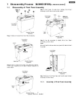
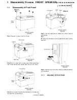
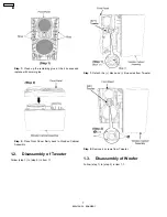
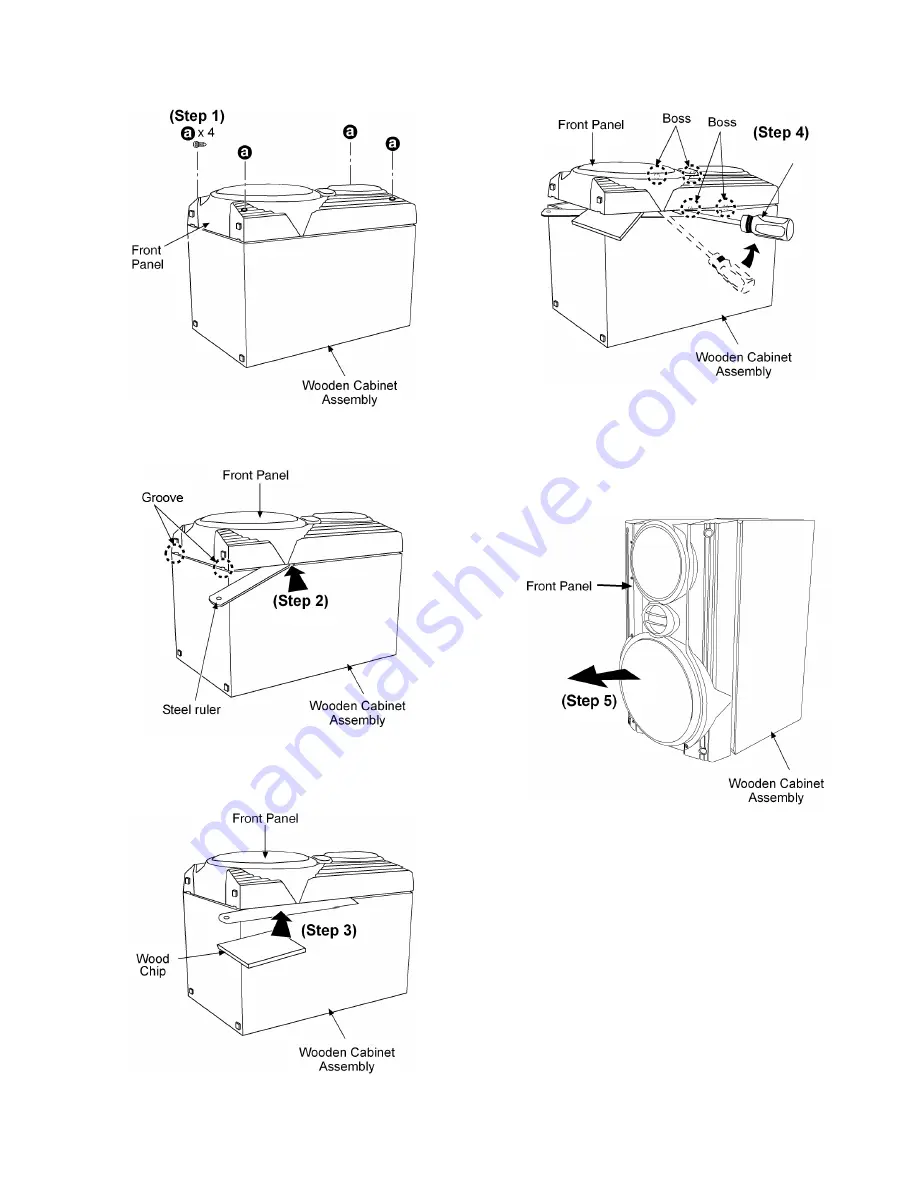
Step 1: Remove 4 screws from Front Panel.

Step 2: Slot in a steel ruler to make a gap allowance between
Front Panel and Wooden Cabinet Assembly as arrow shown.

Step 3: Slot a piece of wood chip in between Front Panel and
the steel ruler as arrow shown.

Step 4: Use the screwdriver to slightly lift up Front Panel as
arrow shown.
Note:
Be careful with the bosses which are glued to Wooden Cabinet
Assembly.

Step 5: Remove Front Panel from Wooden Cabinet Assembly
as arrow shown.

1.1.1. 

Assembly of Front Panel

1.1.  Disassembly of Front Panel

6

service m. speaker

Summary of Contents for SA-TM900DVD

Page 1: ... operarlo lea cuidadosamente este instructivo y consérvelo a la mano para consultas posteriores Información para la región DVD Este DVD esta diseñado y manufacturado para responder a una región de reproducción de DVD Si la región del disco DVD no corresponde a la región del sistema reproductor de discos DVD este no podrá reproducirlo El número de región para este Sistema Estéreo reproductor de DVD...

Page 2: ... 87 5 108 0 MHz paso de 0 1 MHz 8000 W P M P O 450 W CONSUMO DE POTENCIA ALIMENTACION SENSIBILIDAD AUX RANGO DE SINTONIA AM RANGO DE SINTONIA FM DIMENSIONES b x h x l PESO SA TM900DVD SA TM1000DVD ESPECIFICACIONES POR CADA BAFLE FRONTAL SURROUND SUBWOOFER Bocina Super Woofer Bocina Woofer Bocina Tweeter Super Tweeter Alto 4 Ω Bajo 4 Ω 4 Ω 4 Ω 8 Ω CENTRAL SB TM900 1000DVD SB PS92 SB WTM1000 SB PC92...

Page 3: ...0V set to the 127V position Note that this unit will be seriously damaged if this setting is not made correctly There is no voltage selector for some countries the correct voltage is already set 2 Before Repair and Adjustment Disconnect AC power discharge Power Supply Capacitors C5815 C5818 C9513 C9533 C9534 C9816 and C9817 through a 10Ω 5W resistor to ground DO NOT SHORT CIRCUIT DIRECTLY with a s...

Page 4: ...the exposed metal does not have a return path to the chassis the reading must be Figure 1 4 1 2 Leakage Current Hot Check See Figure 1 1 Plug the AC cord directly into the AC outlet Do not use an isolation transformer for this check 2 Connect a 1 5kΩ 10 watts resistor in parallel with a 0 15µF capacitor between each exposed metallic part on the set and a good earth ground such as a water pipe as s...

Page 5: ...ient to damage ES devices 6 Do not remove a replacement ES device from its protective package until immediately before you are ready to install it Most replacement ES devices are packaged with leads electrically shorted together by conductive foam aluminium foil or comparable conductive material 7 Immediately before removing the protective material from the leads of a replacement ES device touch t...

Page 6: ... followings 1 Do not disassemble the optical pick up unit since radiation from exposed laser diode is dangerous 2 Do not adjust the variable resistor on the pick up unit It was already adjusted 3 Do not look at the focus lens using optical instruments 4 Recommend not to look at pick up lens for a long time CAUTION THIS PRODUCT UTILIZES A LASER USE OF CONTROLS OR ADJUSTMENTS OR PERFORMANCE OF PROCE...

Page 7: ...uipped with an anti static flexible cable After replacing and connecting to the flexible board cut the anti static flexible cable Refer to Fig 8 1 Fig 8 1 8 2 Replacing Precautions for Optical Pickup Unit DVD CD Optical Pickup The optical pickup by which part supply was carried out attaches the short clip to the flexible board for laser diode electrostatic discharge damage prevention Please remove...

Page 8: ...9 Accessories Remote control N2QAJB000143 AC cord SJA168 1A FM antenna RSA0006 J AM antenna N1DAAAA00001 Video cable K2KA2BA00001 ...

Page 9: ...10 Operation Procedures 9 ...

Page 10: ...10 ...

Page 11: ...11 Disc information 11 ...

Page 12: ...12 ...

Page 13: ...ns of digital music photography and video on their PC to Create a HighMAT CD or DVD which can be easily played back on consumer electronics devices such as CD and DVD players and car stereos Move digital media files using recordable media such as CD R and CD RW between the PC and various playback devices such as CD and DVD players A new standard for creating personal media on consumer electronic d...

Page 14: ...ad the data 12 3 Benefits of HighMAT Conventional HighMAT Even though DVD player is CD R RW compatible the inconsistent ways that various DVD players can read the music or photos files often leads to a confusing and inconsistant playback experince HighMAT compatible products play content back with consistent interface This includes products which are JPEG compatible products without HighMAT suppor...

Page 15: ...15 ...

Page 16: ...play them back on a DVD player that supports HighMAT you get better easier navigation You get folders you can access with a single click of your DVD player s remote control You can view important information about your music like full song names artist titles album names and genre And you can get faster startup on your home entertainment device To enjoy the benefits of HighMAT all you need is soft...

Page 17: ...d below during repair in order to perform self diagnosis and tilt adjustment effectively Especially when NO DISC is displayed be sure to apply the self diagnosis function before replacing with an optical pickup Replacement of optical pickup generally requires when the present value of laser drive exceeds 45 DVD or 45 CD Note Start diagnosis within three minutes after turning on the power as diagno...

Page 18: ...nds and the power is automatically turned off For F76 Display The abnormalities is an output or the abnormalities in a power supply of POWER AMP IC 14 2 3 Description of Error Code 14 2 3 1 F61 State Condition When the power is turned on the unit is automatically turned off The power does not turn on Cause Troubleshooting Power circuit system failure and or direct current flown to speaker terminal...

Page 19: ...s U H Error U11 Focus servo failure H01 Tray loading failure H02 Spindle servo failure Spindle servo DSC SP motor CLV servo failure H03 Traverse motor failure H04 Tracking servo error H05 Seek timeout failure DSC system F500 DSC failure DSC stops due to servo failure Startup focus failure etc F501 DSC not Ready failure Communication failure between DSC and system computer No communication because ...

Page 20: ...LDO 1 xxx 2 yyyy 3 1 Laser current electricity measurement mode 2 DVD current electricity value 3 CD current electricity value Values are shown in the decimal digit The above example indicates that the current electricity initialization value is 13mA at DVD laser and 32mA at CD laser when laser is turned on Automatically exits the mode after five seconds Measurement of DVD laser current electricit...

Page 21: ... generation 45 y Syscon model type zzz Syscon release number Automatically exits the mode after five seconds Firmware version display While the player is stopped and no disc is inserted press and hold down the button on the player and the number button 7 on the remote controller unit Press Dimmer FL Display button for next page Firmware version display rrr 1 xx 2 y 3 zzz 4 1 Panel computer release...

Page 22: ...ress the STOP or Open button on the player 14 7 CR16 Mechanism Ageing Mode To perform the ageing mode 1 Enter into Test mode 2 Press 3 button on remote control It enters into ageing mode see below for ageing process Ageing process 1 Tray 1 open 2 It waits for one second Note Do not put any disc into the tray 3 Tray close 4 TOC READ Reading incomplete 5 Tray 2 open repeat step 1 to step 4 Process r...

Page 23: ...005 Performing recovery 1 Load the recovery disc Product number RFKZD03R005 to the player and run it 2 Recovery is performed automatically When it is finished a message appears on the screen 3 Remove the recovery disc 4 Turn off the power 15 2 DVD Player Firmware Version Upgrade Process Firmware of DVD player may upgrade to conform to improvement of its performance and quality including operationa...

Page 24: ...screen Remove the disc b Follow the instruction appearing on the screen and remove the disc 6 Turn off the power 15 5 Total Usage Time Display 1 Details of Operation Display Keys for Operation Laser usage time While the player is stopped and no disc is inserted press both the button on the player and the button on the remote controller unit Spindle motor usage time While the player is stopped and ...

Page 25: ...o the Parts No on the page of Parts Location and Replacement Parts List Section 26 if necessary Disassembly of Top Cabinet Disassembly of Rear Panel Disassembly of DVD Changer Unit Disassembly of Main P C B Disassembly of Sub Power P C B Disassembly of Power P C B Disassembly of Transformer P C B Voltage Selector Disassembly of Front Panel Unit Disassembly of Mic P C B Panel P C B Disassembly of D...

Page 26: ...flow chart The following chart is the procedure for disassembling the casing and inside parts for internal inspection when carrying out the servicing To assemble the unit reverse the steps shown in the chart as below 26 ...

Page 27: ...12 screws and disconnect cables CN2810 and CN2813 Fan at rear panel as shown Step 1 Remove 1 screw at rear panel Step 2 Detach the FFC cables CN2810 CN2813 16 3 Disassembly of Top Cabinet 16 4 Disassembly of Rear Panel Follow the Step 1 Step 2 of Item 16 3 Disassembly of Top Cabinet 16 5 Disassembly of DVD Changer Unit Follow the Step 1 Step 2 of Item 16 3 Disassembly of Top Cabinet 27 ...

Page 28: ... and CN2814 Step 5 Remove 2 screws Step 6 Remove the DVD chassis Step 7 Lay the unit For disassembly of DVD mechanism unit please refer to Section 16 16 of this manual 16 6 Disassembly of Main P C B Follow the Step 1 Step 2 of Item 16 3 Disassembly of Top Cabinet Follow the Step 1 of Item 16 4 Disassembly of Rear Panel Follow the Step 1 Step 4 of Item 16 5 Disassembly of DVD Changer Unit 28 ...

Page 29: ...ow shown above Replacement of the Power Amplifier IC Step 1 Desolder the terminals of Power Amplifier IC and replacement the component 16 7 Disassembly of Sub Power P C B Follow the Step 1 Step 2 of Item 16 3 Disassembly of Top Cabinet Follow the Step 1 of Item 16 4 Disassembly of Rear Panel Follow the Step 1 Step 4 of Item 16 5 Disassembly of DVD Changer Unit Follow the Step 1 Step 3 of Item 16 6...

Page 30: ...IC or 1 screw to Voltage Regulator Step 2 Break the joints with a metal cutter as shown below Step 3 Unsolder the terminals of Power Amp IC or transistor to replace the components 16 8 Disassembly of Power P C B Follow the Step 1 Step 2 of Item 16 3 Disassembly of Top Cabinet Follow the Step 1 of Item 16 4 Disassembly of Rear Panel Follow the Step 1 Step 4 of Item 16 5 Disassembly of DVD Changer U...

Page 31: ...p 2 of Item 16 3 Disassembly of Top Cabinet Follow the Step 1 of Item 16 4 Disassembly of Rear Panel Follow the Step 1 Step 4 of Item 16 5 Disassembly of DVD Changer Unit Follow the Step 1 Step 3 of Item 16 6 Disassembly of Main P C B Follow the Step 1 of Item 16 8 Disassembly of Power P C B 16 10 Disassembly of Front Panel Unit Follow the Step 1 Step 2 of Item 16 3 Disassembly of Top Cabinet Foll...

Page 32: ...rd as arrow shown Step 3 Press the 2 catch holders on both sides of the front panel unit to release the claws Step 4 Remove the front panel unit Note Ensure 2 claws on bottom chassis is properly and fully catched to the front panel holes 32 ...

Page 33: ...sideward Step 2 Remove Lid Note Do not misplace the spring 16 11 Disassembly for Mic P C B Panel P C B Follow the Step 1 Step 2 of Item 16 3 Disassembly of Top Cabinet Follow the Step 1 Step 4 of Item 16 5 Disassembly of DVD Changer Unit Follow the Step 1 Step 4 of Item 16 10 Disassembly of Front Panel Unit 16 12 Disassembly of Deck Mechanism Unit Follow the Step 1 Step 2 of Item 16 3 Disassembly ...

Page 34: ...tion of arrow 2 Step 3 Remove Deck Mechanism P C B 16 13 Replacement for Deck Mechanism P C B Follow the Step 1 Step 2 of Item 17 3 Disassembly of Top Cabinet Follow the Step 1 Step 6 of Item 17 5 Disassembly of DVD Changer Unit Follow the Step 1 Step 4 of Item 16 10 Disassembly of Front Panel Unit Follow the Step 1 Step 5 of Item 16 12 Disassembly of Deck Mechanism Unit 16 14 Replacement for Trav...

Page 35: ...Step 2 Remove DVD traverse deck by rotating to the arrow direction 35 ...

Page 36: ... Note Insert a short pin into FFC of the optical pickup See Notice on handling of the optical pickup Step 8 Rotate the traverse deck B to the arrow direction and shift the optical pickup to the furthest backward Step 9 Remove 1 screw 16 15 Replacement for Optical Pickup Unit DVD mechanism Follow the Step 1 Step 2 of Item 16 3 Disassembly of Top Cabinet Follow the Step 1 Step 7 of Item 16 5 Disasse...

Page 37: ...Step 10 Remove the catch of the drive rack and take out the drive rack Step 11 Place the convex part of an optical pickup to the concave part of a traverse base then take out the optical pickup 37 ...

Page 38: ...reparation of gear for servicing perform the procedures as follows In case of re servicing the same set the gear for servicing may be took off because it had been used So the gear for servicing must be stored 1 Remove the gear attached to top cover of CD loading mechanism 2 Insert the hexagonal wrench 2 5mm into the gear 3 Disassemble the body and take out CD loading mechanism 4 Perform disassembl...

Page 39: ...39 ...

Page 40: ...16 17 3 Replacement for the traverse deck Follow the Step 1 Step 10 of item 16 17 2 40 ...

Page 41: ...16 17 4 Disassembly for CD loading unit Follow the Step 1 Step 10 of item 16 17 2 Follow the Step 1 Step 4 of item 16 17 3 41 ...

Page 42: ...42 ...

Page 43: ...43 ...

Page 44: ...ed greases and or oil must be applied when some specific parts are changed 1 Floil grease VFK1298 The floil grease must be applied to tray tray L and tray R 2 Hanarl oil VFK1700 The hanarl oil must be applied to any parts with grease other than the said parts 44 ...

Page 45: ...45 ...

Page 46: ...46 ...

Page 47: ...47 ...

Page 48: ...48 ...

Page 49: ...49 ...

Page 50: ...50 ...

Page 51: ...51 ...

Page 52: ...52 ...

Page 53: ...53 ...

Page 54: ...54 ...

Page 55: ...55 ...

Page 56: ... Follow the Step 1 Step 10 of item 16 17 2 Follow the Step 1 Step 4 of item 16 17 3 16 19 Disassembly for Traverse Unit 56 ...

Page 57: ...rd open the cassette deck For DECK1 and DECK2 Step 2 Push up the cassette lid L R in the direction of arrow For DECK1 and DECK2 16 20 Replacement for cassette lid Follow the Step 1 Step 2 of Item 16 3 Disassembly of Top Cabinet 57 ...

Page 58: ... pinch roller during playback or recording rotate the flywheel F in the direction of the arrow to remove it Step 2 Push the lever upward and open the cassette lid Remove the cassette tape 16 21 Rectification for tape jam problem Follow the Step 1 Step 2 of Item 16 3 Disassembly of Top Cabinet 58 ...

Page 59: ...eck P C B Deck Mechanism P C B Mic P C B Power P C B and Sub Power P C B can be carried out using below procedures For the disassembling procedures refer to Section 16 17 1 Checking of Main P C B 1 Remove Top Cabinet 2 Disassemble DVD Changer Unit 3 Connect FFC cables CN2810 CN2813 from DVD Changer Unit 59 ...

Page 60: ...17 2 Checking of Transformer P C B 1 Remove Top Cabinet 2 Disassemble DVD Changer Unit 3 Connect FFC cables CN2810 CN2813 from DVD Changer Unit 60 ...

Page 61: ...Holder 5 Disassemble Panel P C B 6 Disassemble Deck Mechanism Unit 7 Use the extension cable A to reconnect CN1001 Deck P C B and CP6803 Main P C B 8 Use the extension cable B to reconnect CP6800 Panel P C B and CN971 Deck Mechanism P C B Service Tools Extension FFC A Deck P C B Main P C B REEX0485 14 Pins B Panel P C B Deck Mechanism P C B REEX0484 10 Pins 61 ...

Page 62: ...crews at heat sink and 1 screw at Power P C B 5 Flip the Power P C B 6 Insulate the Power P C B with insulation material to avoid short circuit 7 Use the extension cable A to reconnect CN1001 Deck P C B and CP6803 Main P C B Service Tools Extension FFC A Deck P C B Main P C B REEX0485 14 Pins B Panel P C B Deck Mechanism P C B REEX0484 10 Pins 62 ...

Page 63: ...tape with your finger shown in Fig 3 1 Playback the azimuth adjustment portion 8 kHz 20dB of the test tape QZZCFM in the forward play mode Vary the azimuth adjustment screw until the output of the R CH PB OUT R are maximized 2 Perform the same adjustment in the reverse play mode 3 After the adjustment apply screwlock to the azimuth adjusting screw 18 1 2 Tape Speed Adjustment Deck 1 2 1 Set the ta...

Page 64: ... in Fig 5 from AM SG 4 Adjust Z2602 so that the output frequency is maximized in Fig 6 Fig 5 Fig 6 18 2 2 AM RF Adjustment 1 Connect the instrument as shown in Fig 7 2 Set the unit to AM mode 3 Set AM SG to 520kHz 4 Receive 520kHz in the unit 5 Adjust L2601 OSC so that the EVM AC is maximized 6 Set AM SG to 600Hz 7 Receive 600Hz in the unit 8 Adjust L2601 ANT so that the EVM SG is maximized 9 Set ...

Page 65: ...18 3 1 Cassette Deck Section 18 3 2 Adjustment Point 18 3 Alignment Points 65 ...

Page 66: ...F VREF1 PIN CD SUBSEL TRACKING COIL FOCUS COIL 124 LPC01 Q8551 SWITCH Q8552 SWITCH 126 LPC02 Q8561 SWITCH Q8562 SWITCH 143 AD0 LDCD LDDVD 78 DRV3 QR8571 SUPPLY SWITCH CONTROL HFM VCC OUT 130 VIN9 134 VIN5 129 VIN10 133 VIN6 SUB2 SUB1 123 LPC1 PIN DVD SW 15 1M 8 SUB1 14 SUB2 13 VREF 11 RF 9 FE1 6 FE2 7 TC 4 OPTICAL PICKUP SPINDLE MOTOR UNIT TD 5 TB 2 TA 3 LD DVD 17 LD CD 16 28 R IC8001 DV2 1 MOTOR ...

Page 67: ...44 45 47 48 50 51 53 DQ15 BA0 20 232 BA0 BA1 21 234 BA1 LDQM 15 249 DQM0 UDQM 39 251 DQM1 CS 19 240 NCSM CLK 38 243 MCK 241 MCKI RAS 18 244 NRAS CAS 17 245 NCAS WE 16 248 NWE XWE 11 XCE 26 XOE 28 12 XRESET Q8607 SWITCH Q8606 SWITCH Q8560 SWITCH Q8550 SWITCH R IC8001 DV2 1 MN2DS0003APH 64 SDRAM IC8051 C3ABPG000133 16M FLASH ROM IC8651 RFKWMH82H160 RESET IC IC8601 C0EBE0000384 RESET IC IC8606 C0EBA0...

Page 68: ...15 28 55 P13 149 DAC1OUT 151 DAC2OUT QR8420 MUTING SWITCH 152 DAC3OUT 156 DAC4OUT 158 DAC5OUT 70 P1 69 P2 2 1 68 P3 2 1 5 5 8 5 4 4 A AUDIO DAC IC8421 C0FBBK000050 IC8001 DV2 1 MN2DS0003APH LOGIC IC IC8695 C0JBAA000346 LOGIC IC IC8691 C0JBAA000346 3 3V REGULATOR IC8111 C0CBCBD00018 QR8112 SWITCH QR8111 SWITCH DVD_CLK TO MAIN BLOCK ZERO2 MS MC MD ZFLAG AMUTE 2 3 4 SCK 5 BCK 7 DATA1 6 LRCK 8 S_Y S_C...

Page 69: ... BUFFER COMP FF FF VCO AM MIX AM RM AMP AGC PHASE DET PILOT DET FF PILOT CANCEL FM TUNER 15V SUPPLY SWITCH Q2606 POWER ON RESET UNIVERSAL COUNTER UNLOCK DETECTOR PHASE DETECTOR CHARGE PUMP LC72131MDTRM PLL FREQUENCY SYNTHESIZER IC2602 X2602 16 17 18 11 15 19 10 7 6 9 8 4 CL 3 DI 2 CE 5 DO 13 12 14 20 1 L2602 D2602 L2601 23 24 22 21 20 19 18 17 16 14 15 13 1 2 3 4 6 5 7 8 9 10 11 12 FM IF AMP Q2601...

Page 70: ... MODE_1 S952 HALF X6800 XC_IN 10 XC_OUT 11 X6801 P1 6 40 P35 G1 41 49 G9 SEG34 FL6800 FL DISPLAY REMOTE SENSOR Z6800 JOG VOL VR6800 FROM POWER TRANSFORMER 1 2 58 64 16 23 25 51 SEG0 DIG2 DIG10 23 UP DOWN_F 20 UP DOWN_R 3 OP CL_FWD 2 OP CL_REV OUT2 2 OUT1 4 RM11 UP DOWN MOTOR 9 R_IN 7 F_IN OUT2 2 OUT1 4 RM21 LOADING MOTOR 9 R_IN 7 F_IN IC11 C0GAG0000007 UP DOWN MOTOR DRIVER IC2818 C2CBJG000653 MICR...

Page 71: ...C951 CNB13030R2AU PHOTO INTERRUPTER 89 PHOTO_1 79 PLUNGER_1 Q6801 Q6808 80 PLUNGER_2 78 DECK1_H 10 16 14 13 11 6 19 15 12 21 4 22 3 17 8 1 2 24 23 18 7 9 3 5 2 4 71 REC Q2703 DECK MOTOR SWITCH 74 MOTOR 20 5 M1002 Z971 INTERFACE 91 DECK2 S972 HALF S975 RECINH_F S971 MODE D971 DECK 2 R P HEAD LCH Q6811 LED DRIVE D6809 D6810 S974 RECINH_R B B Q1017 MOTOR SWITCH M DECK 2 ERASE HEAD DECK 1 P B HEAD LCH...

Page 72: ...36 DVD_STAT 35 DVD_CMD 50 DVD_MUTE Q2806 MUTING SWITCH JK2802 COMPONENT VIDEO CB Y CR 68 DVD_PCNT JK2801 S VIDEO OUT IC2006 C9ZB00000466 VIDEO IC IC9500 C0DAAMH00010 REGULATOR G Y C G VIDEO B RED BLUE GREEN Q9504 REGULATOR Q2906 SWITCH YELLOW MIX_MUTE Q2920 MUTING SWITCH DVD_CMD DVD_STAT DVD_CLK IC2803 C0DBEZG00021 REGULATOR B IC2818 C2CBJG000653 MICROPROCESSOR 72 ...

Page 73: ... 63 IC2814 KIA4558FEL DUAL OP AMP C1BB00000979 ANALOG SURROUND IC IC2800 6 7 67 SP_C 66 SP_B 65 SP_A C1BB00000086 SPEAKER ANALYZER IC IC2817 10 11 12 8 AIN SP_A SP_B SP_C 95 SPEAN_A D 17 SPE 76 75 55 MUTE_L JK2803 LINE OUT S6810 S6818 92 KEY1 5 3 7 1 6 2 15 14 LCIN R LOUT R 25 SS_DA DATA 18 24 SS_CLK CLOCK 19 13 COUT 12 SOUT Q2814 MUTING SWITCH Q2813 MUTING SWITCH IC2818 C2CBJG000653 MICROPROCESSO...

Page 74: ... 72 73 CL 46 DA 45 32 28 OUTSUB INCB 6 INLSB 7 INRSB 8 LOUT1 2 59 60 48 ASP_DA 49 ASP_CK DVD_MIXL R DVDFL R DVDSL R SUBW DVDCNT 27 OUTC 39 36 OUTFL R 2 6 1 7 3 5 40 37 FIN4 3 Q2917 MUTING SWITCH 25 23 OUTLS R 41 38 FOUT4 3 2 6 1 7 3 5 IC2818 C2CBJG000653 MICROPROCESSOR 58 MUTE_SUB Q2823 MUTING SWITCH Q2820 SWITCH 59 MUTE_SR Q2818 SWITCH Q2816 MUTING SWITCH 61 MUTEA Q2822 MUTING SWITCH Q2819 SWITCH...

Page 75: ...01 IN_L R 10 14 56 MUTE_H 94 KEY3 S6800 S6809 93 KEY2 B FAN SWITCH Q5801 Q5810 12 RESET RESET OUTL R 4 1 SUBWOOFER L R JK9502 CENTER SUR_L R FRONT L R IN12 12 OUT12 9 LOW L R JK9501 JK9503 ACDET 8 ACDET 6 ACDET 6 FAN Q2913 Q2916 FAN MOTOR DRIVE M B FILTER Q2909 Q2912 FAN MOTOR DRIVE M 5 LATCH 5 LATCH LCH 4 1 OUT_L R LCH LCH FILTER LCH LCH B Q5811 SWITCH IC2818 C2CBJG000653 MICROPROCESSOR FILTER FI...

Page 76: ...STABILISER LIMIT SWITCH 10V VOLTAGE REGULATOR Q2710 D9512 D9517 Q9501 SYSTEM 6V VOLTAGE REGULATOR JK9500 AC INLET FP9500 FP9501 FP5833 SUB TRANSFORMER D9522 D9529 Q5804 Q5806 Q5807 Q5808 Q5803 Q5809 B SYNCHRONISING SWITCH Z9500 D9518 D9521 Q9502 DVD VIDEO SIGNAL LINE DVD AUDIO SIGNAL LINE Q6805 SWITCH Q6804 SWITCH Q6803 SWITCH HP _OUT SYSTEM 6V VOLTAGE REGULATOR SWITCH Q5802 Q5805 RESET Q2702 SWIT...

Page 77: ...20 Voltage Measurement This section is not available at time of issue 77 ...

Page 78: ...tch S6826 Super Sound EQ Switch S6827 S Woofer Switch VR6800 VR Volume Jog The voltage value and waveforms are the reference voltage of this unit measured by DC electronic voltmeter high impedance and oscilloscope on the basis of chassis Accordingly there may arise some error in voltage values and waveforms depending upon the internal impedance of the tester or the measuring unit Importance safety...

Page 79: ...JBC0000105 L2 J0JCC0000307 C5 22P C6 22P C1 0 1 C3 0 1 C2 0 1 R1 0 R4 0 R2 0 C8 0 1 R3 0 R5 0 R6 0 R7 6 8K C7 0 1 VR2 6 8K VR1 6 8K C4 0 22 L3 J0JBC0000105 T F F T HFM TA TB TD TC FE2 FE1 GND IM RF VREF2 RF PIN DVD LD CD LD GND LD DVD GND OEIC VREF1 VCC SUB2 SUB1 PIN CD SW GND IM GND VCC GND GND OUT GND GND TB TA TC TD FE1 FE2 IM RF GND VREF VCC SUB2 SUB1 SW LD CD LD DVD LDGND SCHEMATIC DIAGRAM 1 ...

Page 80: ...2 ERJ3GEY0R00V LB8513 ERJ3GEY0R00V LB8511 ERJ3GEY0R00V LB8514 ERJ3GEY0R00V LB8505 J0JCC0000119 LB8504 J0JCC0000119 LB8503 ERJ2GE0R00X R8501 0 R8506 1 5K C8504 0 1 C8256 0 1 C8257 0 1 R8251 6 8 RX8502 56 x 4 RX8504 56 x 2 RX8503 56 x 2 C8506 100P C8505 220P RX8501 56 x 2 IC8251 C0GBG0000048 DRIVE IC IC8251 TO OPTICAL PICKUP UNIT CIRCUIT ON SCHEMATIC DIAGRAM 1 C8253 16V22 C8255 0 1 C8252 16V47 R8505...

Page 81: ... R8566 56 C8563 6 3V47 R8565 2 2 R8563 1K C8564 1 C8562 16V10 R8564 22 R8562 1K R8561 0 R8560 1K R8569 12K R8570 100K R8550 7 5K C8550 6 3V33 D8550 MA2J11100L C8554 1 QR8571 UNR511V00L SUPPLY CONTROL SWITCH Q8550 2SB1219AHL SWITCH Q8562 2SB09700RL SWITCH Q8552 2SB09700RL SWITCH Q8560 2SD1819A0L SWITCH Q8560 Q8561 2SD1819A0L SWITCH Q8551 2SD1819A0L SWITCH IC8111 C0CBCBD00018 3 3 REGULATOR IC IC8111...

Page 82: ...J2GEJ101X FL8103 F1H0J1050022 FL8102 F1H0J1050022 FL8101 F1H0J1050022 FL8104 F1J1E1040022 VCC GND GND VCC OPU_CPU CLK OPU_CPU CMD OPU_CPU STAT Y PY G CB PB B CR PR R Y C D 1 2V C8695 0 1 C8691 0 1 LB8690 J0JCC0000091 IC8421 IC8691 C0JBAA000346 AND GATE LOGIC IC IC8421 C0FBBK000050 2 CH DAC IC QR8420 UNR521100L AUDIO MUTING SWITCH IC8695 C0JBAA000346 AND GATE LOGIC IC M 9V ZERO2 VOUT1 VOUT2 VCOM AG...

Page 83: ... FDT_7 FDT_14 FDT_6 FDT_13 FDT_5 FDT_12 FDT_4 FDT_11 FDT_3 FDT_10 FDT_2 FDT_9 FDT_1 FDT_8 FDT_0 EXADT_15 EXADR_16 EXADT_14 EXADT_13 EXADT_12 EXADT_11 EXADT_10 EXADT_9 EXADT_8 EXADR_19 EXADR_20 NEXWE EXADR_18 EXADR_17 EXADT_7 EXADT_6 EXADT_5 EXADT_4 EXADT_3 EXADT_2 EXADT_1 EXADT_0 PNRST SCL SDA OPU_CPU CLK OPU_CPU STAT OPU_CPU CMD TRV SW IC8611 C3EBGC000055 16M EEPROM IC NOT SUPPLIED IC8611 IC8651 ...

Page 84: ...11 MDQ_10 MDQ_9 MDQ_8 DQM1 CLK MA_11 MA_9 MA_8 MA_7 MA_6 MA_5 MA_4 MDQ_0 MDQ_1 MDQ_2 MDQ_3 MDQ_4 MDQ_5 MDQ_6 MDQ_7 DQM0 NWE NCAS NRAS NCSM BA0 BA1 MA_10 MA_0 MA_1 MA_2 MA_3 FG C8051 1 C8052 0 1 C8053 220P C8054 1 C8055 1 C8056 0 1 C8057 2200P C8011 1 C8010 0 1 C8008 0 1 C8007 0 1 C8005 0 1 C8009 0 1 C8004 0 1 C8003 2200P RX8011 82 x 4 RX8012 82 x 4 RX8013 82 x 4 IC8051 IC8051 C3ABPG000133 64 SDRAM...

Page 85: ... MDQ19 MDQ28 VDD33 VSS MDQ20 MDQ27 MDQ21 MDQ26 VDD33 MDQ22 MDQ25 MDQ23 VHALF VREFH LPC02 LPC2 LPC01 LPC1 VIN1 VIN2 VIN3 VIN4 RFINP RFINN MUTE124 RAM_CD TRV SW MUTE3 HFMON DRV1 DRV0 PNRST FG OPU_CPU CMD OPU_CPU STAT OPU_CPU CLK KMODE MDQ_9 MDQ_6 MDQ_8 MDQ_7 DQM_1 DQM_0 NWE NCAS NRAS NCSM CLK MA_9 MA_11 MA_8 MA_10 BA0 BA1 MA_7 MA_0 MA_6 MA_1 MA_5 MA_2 MA_4 MA_3 FDT_0 FDT_15 FD_T1 FDT_14 FDT_2 FDT_13...

Page 86: ...8 C8228 1 C8201 6 3V100 C8202 6 3V100 C8206 1 L8201 G1C100K00020 L8202 J0JCC0000079 R8231 10K C8233 4700P C8237 1000P C8238 820P C8236 1000P C8235 1000P R8233 15K R8236 8 2K R8235 8 2K C8232 0 1 C8234 0 1 C8303 0 1 C8312 1 C8304 1 C8311 0 1 R8311 2 4K R8312 1K R8313 24K R8314 0 LB8401 ERJ2GEJ151X C8308 15P R8621 1M R8622 C8622 12P C8621 12P 1K X8621 H0J270500085 C8014 0 1 R8401 47K RX8401 100 x 2 ...

Page 87: ...602 4 7K C2639 50V4 7 C2619 680P C2618 0 01 C2617 0 01 C2642 50V1 R2642 6 8K C2641 50V1 R2641 6 8K R2626 1K R3625 470 R2629 27K R2627 470 C2624 100P R2632 10K C2648 0 01 R3624 33 X2602 H3F1065A0002 C2622 50V1 R3622 2 7K C2621 50V0 47 R2631 120 R2644 120 R2633 1K C2629 6 3V100 C2649 0 1 C2623 50V1 R2645 5 6K C2643 6800P C2644 6800P R2646 5 6K TO MAIN CIRCUIT 1B ON SCHEMATIC DIAGRAM 15 1A 1 2 3 4 CF...

Page 88: ...49 100P C2039 0 01 C2850 100P L2815 J0JCC0000120 C2437 1 C2047 6 3V1000 R2834 100K C2440 0 1 R2822 75 JK2801 C2759 0 01 C2434 6 3V1000 R2830 100K R2810 10K R2807 100K D2909 B0ACCK000005 R2849 1K R2959 2 2 C2965 0 22u R2112 100K R2828 0 R2846 56K R2237 100 C2110 50V47u R2114 47K L2810 J0JBC0000041 R2135 27K C2855 50V4 7 C2236 1000P C2111 1000P R2211 2 7K Q2814 B1GDCFGA0018 MUTING SWITCH R2212 100K ...

Page 89: ...D CB PB B PY Y G YGND YGND CR PR R SL D 5V SUBW D 5V FR ADACGND ZFLAG ADACGND SR ADACGND DGND DGND A 5V AGND DGND DGND CENTER ADACGND D 5V MOT10V DVD_STA DVD_CMD DVD_CLK FRONT_R FRONT_L SL S_C S_Y CR_R CB_B PY ADAC5V CENT SUBW SR MIX_R MIX_L Q2806 D2836 B0EAKM000117 R2814 10K C2500 16V10 C2200 50V1 C2100 50V1 C2312 16V10 R2827 0 CN2813 C2600 50V10 C2400 16V10 TO CD LOADING CIRCUIT CN1 ON SCHEMATIC...

Page 90: ...68 R2945 0 C2103 16V10 R2956 220 C2931 1000P R2942 4 7K C2904 2700P R2938 3 9K C2202 16V10 C2102 16V10 R2863 0 R2553 100 9 0V KA_ROUT 9 0V KA_LOUT LINE_LOUT LINE_ROUT R2059 0 R2209 12K R2107 47K R2210 100K R2110 100K C2104 16V10 C2106 10P R2207 47K C2107 0 01 C2206 10P C2205 50V33 R2109 12K R2108 3 3K R2208 3 3K C2204 16V10 R2106 1K C2208 50V47 C2108 50V47 R2206 1K IC2814 KIA4558FEL DUAL OP AMP C2...

Page 91: ...8 MUTING SWITCH IC2815 KIA4558FEL DUAL OP AMP R2510 27K R2855 56K R2310 270 R2407 56K Q2825 B1ABEB000002 SWITCH R2228 3 3K C2229 1000P C2228 50V1 0 C2864 16V10 C2128 50V1 R2623 27K R2128 3 3K Q2823 B1GDCFGA0018 MUTING SWITCH R2410 270 R2126 8 2K R2620 56K C2310 50V1 R2307 56K R2615 6 8K C2603 50V3 3 C2130 100P R2406 1 8K C2129 33P R2508 56K CN2802 Q2820 B1ABEB000002 MUTING SWITCH C2604 1000P R2619...

Page 92: ...7 5V 7 5V LINE_ROUT LINE_LOUT EXT_L EXT_R SS_S SS_C LIN MICIN LF RSIN LSIN RCIN LCIN SF RIN RF DGND AGND SOUT ROUT COUT VCC VEE CLOCK LOUT DATA IC2800 C1BB00000979 ANALOG SURROUND IC C2114 10V1 C2857 16V10 R2091 0 C2140 0 082 C2138 16V10 C2238 16V10 R2139 12K C2237 0 022 C2320 10V0 1 R2115 8 2K R2239 12K C2213 0 15 C2112 50V1 C2212 50V1 C2522 10V0 1 C2137 0 022 C2239 3300P R2215 8 2K C2858 16V10 C...

Page 93: ...01 R2061 0 CP6803 R2229 100 R2238 33K R2231 33K Q2704 B1GDCFJJ0047 MOTOR SWITCH R2064 0 R2606 10K R2066 0 R2129 100 C2234 1000P PBL 9 0V DCDET FAN R2590 0 R2068 0 C2986 16V10 Q2911 2SB0709AHL FAN MOTOR DRIVE R2587 2 2M R2581 1 2K Q2910 2SD0601AHL DETECT SWITCH R2592 100K D2914 CN2815 R2588 4 7K R2582 100K Q2909 2SD0592ARA SWITCH R2593 4 7K C2983 0 01 R2589 3 3K R2583 220K R2585 120K C2987 10V10 C2...

Page 94: ...6 0 C2722 10V22u R2688 100K C2961 1000P C2725 100P R2847 10K R2911 47K R2748 10K R2957 680 C2746 0 01 R2723 22K C2743 1000P R2926 100 C2724 100P R2990 10K R2798 100 C2749 50V0 1 C2977 470P R2685 100K C2973 16V100 C2728 100P D2910 B0ACCE000003 R2792 1K C2981 470P R2912 47K C2723 100P C2744 0 01 C2747 50V0 1 C2748 50V0 1 C2721 0 01 L2802 ERJ3GEY0R00V R2662 4 7K D2908 B0ACCK000005 R2910 4 7K C2720 47...

Page 95: ...0P R2790 1K R2738 1K C2750 100P R2776 1K R2733 1K C2705 100P C2711 100P R2737 1K R2917 10M C2710 100P R2864 0 X6801 H0A327200115 C2713 1000P C2734 39P R2747 4 7K C2714 100P C2737 15P C2712 1000P R2793 100 R2089 0 C2978 100P C2704 100P R2742 1K C2716 100P R2088 0 R2788 100K R2778 100 R2752 100 R2735 10K X6800 H2A1005A0005 R2732 1K R2750 1K R2077 0 R2784 100 R2782 1K R2739 1K R2789 100 IC2818 C2CBJG...

Page 96: ...F_1 MODE_1 PLUNGER2 PLUNGER1 PHOTO_2 PHOTO_1 HP_MUTE JOG_B JOG_A KEY3 KEY2 ED_A E_CLK E_CS VREF VREF SYNC DATA CLK R2999 0 D2905 B0ACCK000005 Q2702 B1GBCFJJ0051 SWITCH R2072 0 C2732 0 01 R2922 22K R2920 10K IC2816 C3EBEG000072 EEPROM IC NOT SUPPLIED C2733 50V2 2 R2913 10K C2738 0 022 R2667 22K Q2710 B1GBCFJJ0051 SYNC SWITCH C2739 330P D2906 B0ACCK000005 R2914 4 7K C2741 35V4 7 CN2811 C2740 330P R2...

Page 97: ...6809 STOP S6808 FF S6807 REW S6806 DECK 2 R6854 1K R6855 1K R6856 1 2K R6858 2 2K R6857 1 8K S6800 DVD CD S6801 TAPE S6802 TUNER BAND S6803 AUX S6804 DECK 1 S6805 DISPLAY DEMO R6970 6 8K R6969 4 7K R6968 2 7K R6967 2 2K R6963 1K R6964 1K R6965 1 2K R6966 1 8K S6827 SUBWOOFER S6826 SUPER SOUND EQ S6825 DISC1 S6824 DISC 2 S6819 OPEN CLOSE S6820 DISC CHANGE S6821 DISC 5 S6822 DISC 4 S6823 DISC 3 R682...

Page 98: ...17 P18 P19 P20 P21 P22 P23 P24 P25 P26 P27 P28 P29 P30 P31 P32 P33 P34 P35 VREF RMT DVREF PCONT VREF SYS6V Z6800 B3RAB0000025 REMOTE SENSOR DGND RMT FLD_CS FLD_RST FLD_CK FLD_DA PCONT SYNC SW5V DCDET 9 0V SYS6V 9 0V MOT10V VREF DVREF DECK2 HALF_1 MODE_1 PLUNGER2 PLUNGER1 PHOTO_2 PHOTO_1 JOG_B JOG_A GND2 KEY3 KEY2 KEY1 HP_MUTE MIC MIC_GND HPOUT_FR HPOUT_FL TO MAIN CIRCUIT CN2811 ON SCHEMATIC DIAGRA...

Page 99: ... Q1003 B1AAGC000007 SWITCHING RECH Q1007 R1090 220 C1046 16V220 R1040 0 C1044 10V33 R1004 1 5K Q1004 Q1005 Q1004 Q1005 B1AAGC000007 BIAS OSCILLATOR C1013 1000P C1014 1000P C1010 25V100 R1007 4 7 C1016 2200P C1017 2200P R1011 8 2K Q1007 B1ABCF000176 BIAS OSC CONTROL C1026 6 3V47 R1013 4 7K R1012 4 7K C1018 3300P R1014 4 7K C1011 0 047 C1008 50V1 C1034 50V3 3 R1032 10K R1055 2 2K C1038 220P C1042 16...

Page 100: ...NE IC951 CNB13030R2AU PHOTO INTERRUPTER IC971 CNB13030R2AU PHOTO INTERRUPTER Z971 RGSD12A1445T MODE PL GND HALF STBY_5V VREF_GND PHOTO_T D1_CRO2 TO PANEL CIRCUIT CP6800 ON SCHEMATIC DIAGRAM 19 MODE PL GND HALF PHOTO_S STBY_5V VREF_GND PHOTO_T D1_CRO2 DECK MECHANISM CIRCUIT CN971 PL1 PL2 STBY_5V PL_GND AD_OUT PHOTO_PB PHOTO_RP HALF_PB VREF_GND MODE_PB R972 820 R973 39K PL971 R952 820 R953 39K D951 ...

Page 101: ... H5803 H5901 D5821 D5820 W2 W2A W1A R5107 R5207 R5104 R5204 R5101 D5801 R5891 C5805 R5892 C5812 D5802 C9533 C9534 R5201 E5801 CN5802 C5803 C5801 C1002 C1001 D5809 W1 Q5801 Q5810 Q5811 H9500 D5803 C5818 R5835 C5808 R5105 C5103 C5102 R5820 R5822 R5809 R5821 R5816 C5815 R5103 R9534 R9535 R9536 R5203 R5205 C5202 C5203 C5807 R5815 R9532 R9531 R5866 R5504 R5898 R5501 R5301 R5500 R5400 R5401 R5300 R5302 ...

Page 102: ...6CC 6CC 54 4 4 54 6CC 2 2 6 6CC 2 54 54 4 6 7 7 7 7 0 0 0 0 23 0 2 2 2 2 1 1 1 2 2 2 2 2 2 2 2 2 2 2 2 2 2 6 4 54 4 2 ...

Page 103: ... 54 2 352 4 352 2 35 7 2 54 7 54 6CC 2 54 2 7 7 7 7 9 9 2 3 6 4 2 2 2 2 2 2 7 7 2 2 2 2 2 2 2 2 2 2 2 2 7 7 2 ...

Page 104: ... 6CC 2 2 6 6 7 2 54 7 54 6CC 352 4 352 2 35 6CC 6CC 352 2 4 352 4 4 4 4 4 4 6CC 4 6CC 6 P P 0 0 6 0 0 0 23 0 9 9 2 2 2 2 2 2 2 2 2 2 2 2 2 2 2 7 2 72 7 7 7 2 54 54 4 4 4 6 4 6CC 32 3 3YM ATE 2E _ _ _ _ _ _ _ _ _ _ _ _ _ _ _ _ ...

Page 105: ...6CC 6CC 54 6CC 6CC 54 4 54 54 6CC 54 4 2 0 352 2 4 2 352 2 352 4 2 352 P P P 23 0 2 2 2 2 2 2 2 4 53 2 4 3 32 54 4 2 352 2 352 3352 352 2 4 2 8 9 PPROVED HECKED EVISION HANGED ROM 3IGND ...

Page 106: ... 6 37 6 6 6 7 6 0 6 K 2 2 2 2 2 2 2 2 2 1 2 2 1 2 2 2 1 2 2 2 1 2 2 2 2 2 2 6 6 6 0 4 6 3 7 2 6 4 2 4 6 37 6 6 U0 4 2 6 0 4 2 4 4 3 23 6 4 6 6 ...

Page 107: ...35 6 6 7 7 7 7 7 7 6 U 2 2 2 0 2 1 2 2 1 2 2 1 2 1 2 2 2 4 6 35 ...

Page 108: ...6CC 6CC 6CC 35 6CC 6CC 0 6CC 6 6 6 3 9 7 7 35 6CC 6CC 6CC 6 6CC 6CC 6CC 35 6CC 0 0 6CC 6CC 6 6 0 4 3ECTION TEM OR ODE O 3YM SSUED 0RE 42 3 ...

Page 109: ...0 7 7 7 2 2 2 3 4 6 EW ODEL GT IC OTE ATERIAL 3IZE MODIFIED 0 4 25 ...

Page 110: ...2 0 7 2 0 5NIT MM 0ARTS NO AME PPROVED HECKED 3 ...

Page 111: ......

Page 112: ......

Page 113: ......

Page 114: ......

Page 115: ......

Page 116: ...116 ...

Page 117: ...117 ...

Page 118: ...9512 B0EAKM000125 D9517 B0EAKM000125 C9510 25V470 C9511 25V470 D9509 B0EAKM000125 R9504 1 5K R9505 1 2K C9503 1000P R9503 820K D9510 B0AACK000004 D9511 B0EAKM000125 C9502 0 01 D9515 B0BA7R000005 F1 250V 4A FC2 FC1 Z9500 ERZV10V511CS TO POWER CIRCUIT H9500 ON SCHEMATIC DIAGRAM 23 FL_GND FL2 FL1 PCONT SYS6V SYNC VP DGND DVD_PCONT DVD_AC D 5V DGND SUB B VccH VccH VccL AC_GND AC_GND VccL VccH VccH AC_...

Page 119: ...OUT2 RNF OUT1 VM VCC F_IN GND R_IN VREF OUT2 RNF OUT1 VM VCC F_IN GND R_IN IC11 C0GAG0000007 UP DOWN MOTOR DRIVE IC21 C0GAG0000007 LOADING MOTOR DRIVE S3 BOTTOM S4 OPEN S1 STOCK S2 PLAY B SIGNAL LINE TO MAIN CIRCUIT CN2810 ON SCHEMATIC DIAGRAM 11 CN1 S5 CHANGE 7 5V PGND CR16 SWITCH DGND UP DOWN F UP DOWN R BOTTOM SW POSTION SENS LED OPEN SW LOAD F LOAD R STOCK SW PLAY SW 1 2 3 4 5 6 7 8 9 1 2 3 4 ...

Page 120: ...232 C8207 C8026 C8024 C8307 SIDE A X X TL8513 TL8522 X TL8512 X X X TL8201 CL8551 CL8561 X CL8233 X X CL8234 CL8236 X X CL8231 CL8235 X X CKC1 CKC2 X X X X CKC8 CKC10 CKC4 CKC6 X X X X CKC11 CKC12 CKC14 CKC16 X X X X X CKC15 CKC18 CKC20 CKC22 CKC24 X X X X CKC32 CKC36 CKC37 CKC40 X X X X CKC44 CKC48 CKC49 CKC50 X X X CL8430 X CL8421 X X X CL8424 CL8425 CL8426 CKC41 CKC45 X X CL8040 CL8491 CKB1 CKB...

Page 121: ...562 Q8606 Q8607 QR8420 R8021 R8022 R8023 R8243 R8251 R8261 R8263 R8313 R8314 R8420 R8553 R8554 R8555 R8556 R8557 R8558 R8559 R8563 R8564 R8565 R8566 R8567 R8568 R8601 R8606 R8607 R8621 R8622 X8621 QR8112 QR8111 R8112 R8111 RX8014 RX8013 C8057 C8056 C8055 C8054 C8053 C8052 C8051 IC8051 FP8501 TO OPTICAL PICKUP UNIT C8006 C8007 C8008 C8009 C8010 C8651 C8652 IC8651 RX8011 RX8012 RX8021 R8312 R8311 C8...

Page 122: ... D2909 R2849 C2903 C2234 C2134 R2233 R2133 R2060 R2624 R2553 R2 R2202 R2102 R2213 R2155 R2130 R2230 R2998 R2 W2104 R2862 R2096 R2097 Q2917 R2691 R2692 R2113 R2254 Q2919 R3630 R3631 R3634 W2131 W2130 R3633 W210 W2101 W2126 R3627 R3626 W2127 W2128 K2906 K2905 W2099 W2096 W2095 W2094 W2091 W2090 R2693 C2650 W2087 R3640 R3641 R3642 D29 W3002 W3003 C2620 C2621 C2622 W2443 X2603 C2630 W2441 W2442 W2440 ...

Page 123: ... R2077 Q2823 Q2816 Q2815 Q2822 R2854 R2620 R2852 R2856 C2903 R2702 R2988 R2859 R2851 R2589 R2590 Q2920 R3628 R3629 R3634 W2132 R3633 C2719 W2133 W2103 W2101 R2762 C2754 R3637 R3639 R3638 C3623 R3642 D2915 D2914 D2916 D2917 D2918 D2919 K9999 W2999 W3011 W2125 W3005 W3004 R2754 R2793 9 C2615 W2434 3 W2432 C2614 W2430 W2429 W2428 W2427 C2627 Q2606 W2415 W2414 W2413 W2410 W2431 CF2602 K2902 W2760 W276...

Page 124: ...808 L6803 L6802 L6804 Q6810 W6854 W6855 C6800 C6802 W6825 C6853 Z6800 W6811 W6826 W6827 W6812 C6804 W6856 C6856 W6813 W6814 W6815 R6960 R6959 L6801 C6854 W6857 W6816 L6805 W6852 W6862 W6801 W6802 W6832 W6833 W6820 W6834 W6866 W6822 W6871 W6851 W6872 W6874 W6875 W6877 W6878 W6881 W6900 W6823 W6903 W6904 W6905 W6912 W6913 K6801 K6804 W6917 W6918 W6817 D6810 W6885 R6970 R6969 R6968 R6967 R6966 R6965 ...

Page 125: ...5 W6806 W6807 H6807 W6863 W6808 W6839 W6840 W6841 W6842 W6860 Q6804 Q6805 Q6803 W6828 W6829 W6861 W6862 W6818 W6803 W6831 W6819 W6832 W6833 W6820 W6834 C6813 C6855 W6866 W6821 W6822 W6870 W6851 W6872 W6874 W6864 W6876 W6875 W6877 W6878 W6879 W6880 W6881 BS6800 H6810 W6823 W6904 W6905 W6909 W6910 W6911 W6913 W6914 D6809 W6883 W6884 R6937 R6938 R6939 R6940 R6941 R6942 R6943 R6944 R6829 R6856 R6857 R...

Page 126: ...A A A CA A B C E B C E B C E JK6802 JK6800 C6879 C6865 R6892 R6888 R6981 C6871 C6873 C6875 R6891 R6987 C6872 C6882 R6886 R6994 C6881 R6982 C6866 C6867 W6800 C6876 R6890 R6983 C6811 L6809 H6805 R6887 C6870 L6806 K6806 C6868 Q6806 Q6807 Q6817 R6991 R6993 R6992 W6890 W6891 R6995 MIC1 MIC2 PbF D1 R1 C1 Q1 R4 Q2 L1 R6 R5 D2 C3 C4 C5 C6 C7 C8 C9 C10 C11 R7 R8 R9 R10 Q3 Q4 D3 R11 L2 C2 R3 R2 J1 J2 J3 J4 ...

Page 127: ...J1008 J1009 C1010 J1111 J1011 J1020 J1012 J1013 J1022 J1028 J1038 J1014 J1033 J1023 J1021 J1015 C1046 Q1005 R1007 W1002 CS1002 TO R P HEAD CS1001 TO P B HEAD L1002 IC1004 C1041 CN1001 J1010 J1004 C1030 C1032 C1045 C1033 C1037 C1056 C1031 C1035 C1042 J1064 J1051 L1001 Q1004 J1006 J9999 R1005 R1003 C1021 R1010 R1097 R1004 C1016 R1060 C1017 C1020 R1009 C1014 C1013 C1019 R1018 C1057 C1038 C1036 R1032 ...

Page 128: ...857 R5821 R5820 R5809 R5822 R5906 W5879 C5810 FP5833 0 4A R5826 R5827 R5830 C5812 W5872 R5829 C5805 Q5805 C5808 C5802 R5847 W5878 W5887 W5886 W5880 W5885 W5875 R5824 C5801 D5806 D5805 W5883 W5884 W5858 W5882 W5860 W5861 W5859 W5854 W5855 W5856 W5862 W5850 W5876 W5888 W5870 W5871 W5866 W5873 W5865 W5864 W5863 W5868 W5836 W5903 W5902 W5901 W5904 Q5804 W5877 Q5808 W5853 H5900 CN5802 E5801 W5881 W5889...

Page 129: ...1 W5845 W5846 W5847 W5857 R5821 R5820 R5809 R5822 C5812 W5849 W5860 W5861 W5859 R9523 R5105 R9528 R5205 L9502 L9507 C5813 W5852 W5851 W5832 W5839 C5807 C5834 W5840 W5833 W5835 W5837 W5834 W5854 W5855 W5856 W5862 W5850 W5870 W5866 W5863 W5844 W5843 W5842 W5841 W5838 W5904 W5853 C5815 C5818 IC5001 JK9503 JK9501 R9525 L9504 R5606 L9503 R9524 R5605 L9505 R9526 R5705 W5831 R5703 RIGHT SPEAKER LEFT SPEA...

Page 130: ...9529 Z9500 W9521 W9520 R9500 D9508 D9514 C9509 D9513 C9512 R9521 FP9500 1A R9520 R9519 D9516 C9517 Q9503 C9505 FP9501 4A C9506 C9513 D9504 W9519 W9511 W9514 W9515 W9510 W9509 C9501 W9517 W9516 D9500 W9518 Q9500 R9518 W9506 W9507 W9508 W9513 R9516 R9515 R9507 R9512 R9514 R9513 R9509 R9511 R9522 R9510 IC9500 L9500 C9515 D9503 D9502 C9507 D9501 W9502 Q9504 C9514 R9508 CN9500 R9517 W9503 W9531 W9504 W...

Page 131: ... F G 1 2 3 4 5 6 7 8 9 J PbF CN1 RM21 IC21 C22 C21 LOADING_MOTOR OPENSW STOCKSW S1 PLAYSW S2 RM11 UP DOWN_ MOTOR IC11 C12 C11 Q1 BOTTOMSW S4 J21 J11 J13 J14 J12 S3 J15 J16 CHANGESW S5 M M 14 9 1 2 3 4 5 6 7 8 9 10 11 12 13 8 7 6 5 4 3 2 1 1 2 3 4 5 6 7 8 9 131 ...

Page 132: ...220 240V 50 60HZ CAUTION RISK OF ELECTRIC SHOCK AC VOLTAGE LINE PLEASE DO NOT TOUCH THIS P C B T9501 SUB TRANSFORMER T9500 POWER TRANSFORMER JK9500 S5950 7 CN9500 CN5804 1 PbF A DVD MODULE P C B SIDE A PbF PbF PbF FP8101 1 50 FP8201 6 1 TO SPINDLE MOTOR MIC P C B SOLDER SIDE D MIC 2 MIC 1 H6805 JK6800 JK6802 5 1 PbF PbF H6806 5 1 H5804 11 1 H5803 10 1 JK9502 RIGHT SURROUND SPEAKER CENTER SPEAKER L...

Page 133: ... 2 1 CN2814 3 1 CF2602 1 3 L2601 L2602 Z2602 A DVD MODULE P C B SIDE A TO OPTICAL PICKUP UNIT FP8501 25 1 26 2 E DECK P C B SOLDER SIDE SOLDER SIDE G POWER P C B CN5801 H5900 1 12 11 1 H5901 10 1 CN5800 1 12 J CD LOADING P C B SOLDER SIDE PbF PbF PbF PbF PbF RM21 LOADING MOTOR RM11 UP DOWN M M CN1 13 1 14 2 W1002 1 2 MOTOR CS1002 DECK 2 R P HEAD ERASE HEAD 1 2 5 4 CS1001 DECK 1 PLAYBACK HEAD 1 2 5...

Page 134: ... UNR521400L UNR521100L 1 24 25 48 1 5 6 C0DBEZG00021 6P B1GFGCAA0001 B0ACCE000003 B0BC010A0007 B0BC01600013 MA2J11100L RSN315H42C P 1 2 3 C0EBE0000384 RFKWMH82H160 1 4 8 5 C0AABA000009 C1AA00000612 1 5 1 C0HBB0000039 64P MN2DS0003APH 256P C2CBJG000653 100P C1BB00000845 56P C1BB00000801 80P AN7348S E1 24P C0FBBK000050 28P C1BB00000086 18P C3ABPG000133 54P KIA4558FEL 8P LA1833NMNTLM 24P LC72131MDTRM...

Page 135: ...B0ACCK000005 MA2J72800L Cathode Anode Ca A B0AACK000004 MA2C16500E B0JAPG000019 A Ca Cathode Anode 135 ...

Page 136: ...al for the EEPROM Pin No Mark I O Function 39 ECLK O CLOCK Signal for the EEPROM 40 ECS O CHIP SELECT Signal for the EEPROM 41 EFP_EPM O For Flash 42 FLD_RST O Reset Signal for the FL DRIVER 43 FLD_CS O Latch Signal for the FL DRIVER 44 FLD_DA O Data input for the FL DRIVER 45 FLD_CK O Clock Signal for the FL DRIVER 46 EFP_CE O For Flash 47 Wide1 O S Video output control 48 ASP_DA O DATA signal fo...

Page 137: ...Tuner Region Setting 2 88 REG3 I Tuner Region Setting 3 89 PHOTO_1 A D I Rotating Detection Signal Deck 1 90 PHOTO_2 A D I Rotating Detection Signal Deck 2 91 DECK2_AD A D I AD input from DECK2 RINHF MODE2 RINHR HA LF2 92 94 KEY1 KEY3 A D I Key 1 to Key 3 input 95 SPEANA_AD A D I Signal from Speana IC s OUT port 96 AVSS ANALOG POWER SUPPLY INPUT 97 DVD_RS A D I DVD Region Setting 98 VREF REFERENCE...

Page 138: ... otherwise P Pico farads pF F Farads Resistance values are in ohms unless specified otherwise 1K 1 000 OHM The marking RTL indicates that the Retention Time is limited for this items After the discontinuation of this assembly in production the item will continue to be available for a specific period of time The retention period of a availability is dependent on the type of assembly and in accordan...

Page 139: ...26 1 Deck Mechanism RAA3413 S 26 1 1 Deck Mechanism Parts Location 139 ...

Page 140: ...140 ...

Page 141: ... M 118 RML0372 WINDING LEVER M 119 RML0374 EJECT LEVER M 120 RMM0131 BRAKE ROD M 121 RMM0133 1 EJECT ROD M 122 RMQ0519 REEL HUB M 123 RMS0398 1 MOVING CORE M 124 RSJ0003 PLUNGER ASS Y M 125 RMC0061 PACK SPRING M 126 RXF0049 FLYWHEEL F ASS Y M 127 RXF0050 FLYWHEEL R ASS Y M 128 RXG0040 FF RELAY GEAR ASS Y M 129 RMK0283A J SUB CHASSIS M 130 RXL0124 PINCH ROLLER F ASS Y M 130 1 RMB0401 PINCH ARM SPRI...

Page 142: ...26 2 DVD Loading Mechanism 26 2 1 DVD Loading Mechanism Parts Location 142 ...

Page 143: ...143 ...

Page 144: ...N SW LEVER M 337 RML0624 CHG LEVER M 338 RML0701 TRAY STOPPER M 339 RMM0239 1 UD RACK L M 340 RMM0240 UD RACK R M 341 RMM0290 TRV SLIDE PLATE L M 342 RMM0242 1 TRV SLIDE PLATE R M 343 RMM0243 SELECT RACK M 344 RMM0244 SELECT GUIDE M 345 RMQ1051 2 PITCH PLATE M 346 RMQ1461 UD BASE M 347 RMQ1056 TRAY GUIDE L M 348 RMQ1057 TRAY GUIDE R M 349 RMQ1058 GEAR HOLDER M 350 RMQ1059 2 TOP COVER M 351 RMQ1060...

Page 145: ...26 3 Cabinet 26 3 1 Cabinet Parts Location 145 ...

Page 146: ...146 ...

Page 147: ...147 ...

Page 148: ...32 K CONTROL BUTTON M 27 RGUX0633 K F BTN CAP A AUX M 28 RGUX0634 K F BTN CAP B FM M Ref No Part No Part Name Description Remarks 29 RGUX0635 K F BTN CAP C TAPE M 30 RGUX0636 K F BTN CAP D CD DVD M 31 RGWX0072 S VOLUME KNOB M 32 RHD26046 SCREW M 33 RHD30004 2S SCREW M 34 RHD30119 S SCREW M 35 RHDX30006 STEP SCREW M 36 RKA0072 KJ LEG CUSHION M 37 RKFX0129 S CASSETTE LID L M 38 RKFX0130 S CASSETTE L...

Page 149: ...M RHD26046 SCREW M RHD30004 2S SIDE SCREW M RHD30119 S SCREW M RKA0072 KJ LEG M RMCX0021 J TRANSISTOR CLIP M RMNX0133 1 MIC JACK HOLDER M RXXX0065 HEATSINK UNIT M RYKM0041 TOP CABINET BENT M SHR301 J LEAD CLAMPER M T2KA02916 SOLDADURA ROLLO PB FREE 1 6 M XTB3 10JFJ TORNILLO M XTW3 15TFJ TORNILLO M L6FALEFH0030 VENTILADOR M RMNX0019 PCB SPACER M RTPM1P3M045 V Transformador M RZGGHG308 GRASA DISIPAD...

Page 150: ...1 M RPNM0155 T UNICEL SA TM850 900 950 1000 M RQAM0119 POLIZA DE GARANTIA M RQZM0195 ETIQUETA NUMERO DE SERIE SA TM900 M RQLM0285 ETII SERIE BLANCA TM22 M TPS1 1A CINTA DIUREX M RZTM0005 B CINTA P CAJA M SW743734 GRAPA M RPNM0155 B 1 UNICEL SA TM850 900 950 1000 M CONJUNTO EMPAQUE SA TM900 ...

Page 151: ...VC1H101K CHIP RESISTOR M C2122 ECJ1VC1H470K CHIP RESISTOR M C2123 ECJ1VB1H103K CHIP CAPACITOR M C2124 F1H1C223A001 CHIP RESISTOR M C2128 ECEA1HKA010B CAPACITOR M C2129 ECJ1VB1H102K CHIP CAPACITOR M C2130 ECJ1VC1H101K CHIP RESISTOR M C2131 ECEA1HKA010B CAPACITOR M C2134 ECJ1VB1H102K CHIP CAPACITOR M C2136 ECJ1VC1H102J CHIP CAPACITOR M C2137 ECJ1VB1H223K CAPACITOR CHIP M C2138 ECEA1CKA100B CAPACITOR...

Page 152: ...6 ECJ1VC1H100D CAPACITOR M C2517 ECEA1HKAR47B CAPACITOR M C2522 ECJ1VB1C104K CAPACITOR M C2600 ECEA1HKA100B CAPACITOR M C2601 ECJ1VB1H103K CHIP CAPACITOR M C2602 ECEA1HKA010B CAPACITOR M C2603 ECEA1HKA3R3B CAPACITOR M C2604 ECJ1VB1H102K CHIP CAPACITOR M C2605 ECJ1VC1H101K CHIP RESISTOR M C2606 ECEA1HKA100B CAPACITOR M C2607 ECJ1VB1C104K CAPACITOR M C2608 ECEA1HKAR47B CAPACITOR M C2609 ECEA1HKA100B...

Page 153: ... M C2732 ECJ1VB1H103K CHIP CAPACITOR M C2733 ECEA1HKA2R2B CAPACITOR M C2734 ECJ1VC1H390J CHIP CAPACITOR M C2735 ECJ1VC1H390J CHIP CAPACITOR M C2736 ECJ1VC1H180J CHIP CAPACITOR M C2737 ECJ1VC1H180J CHIP CAPACITOR M C2738 ECJ1VB1C223K CAPACITOR M C2739 ECJ1VC1H331J CHIP CAPACITOR M C2740 ECJ1VC1H331J CHIP CAPACITOR M C2741 ECEA1VKA4R7B CAPACITOR ELECTROLITICO M C2742 ECJ1VB1H103K CHIP CAPACITOR M C2...

Page 154: ...A101B CAPACITOR M C2935 ECJ1VB1H104K CAPACITOR CHIP M C2936 ECEA1HKA2R2B CAPACITOR M C2937 F1H1H332A013 CHIP RESISTOR M C2938 ECJ2VB1C154K CAPACITOR CHIP M C2939 ECEA1HKA010B CAPACITOR M C2940 ECEA1HKA010B CAPACITOR M C2941 ECEA1HKA010B CAPACITOR M C2942 ECJ1VB1H102K CHIP CAPACITOR M C2943 ECJ1VB1H102K CHIP CAPACITOR M C2944 ECJ1VB1H123K CHIP CAPACITOR M C2947 ECJ1VC1H102J CHIP CAPACITOR M C2948 E...

Page 155: ... C5502 ECJ1VB1H104K CAPACITOR CHIP M C5503 ECJ1VB1H104K CAPACITOR CHIP M C5600 ECJ1VB1H821K CHIP CAPACITOR M C5601 ECJ1VC1H150J CHIP CAPACITOR M C5602 ECJ1VB1H104K CAPACITOR CHIP M C5603 ECJ1VB1H104K CAPACITOR CHIP M C5604 ECJ1VB1H104K CAPACITOR CHIP M C5605 ECJ1VB1H104K CAPACITOR CHIP M C5700 ECJ1VB1H821K CHIP CAPACITOR M C5701 ECJ1VC1H150J CHIP CAPACITOR M C5702 ECJ1VB1H104K CAPACITOR CHIP M C57...

Page 156: ...PACITOR M C6895 ECA1CAK100XB CAPACITOR ELECTROLITICO M C6896 ECJ1VC1H101K CHIP RESISTOR M C6897 ECJ1VC1H101K CHIP RESISTOR M C6898 F1H1H332A013 CHIP RESISTOR M C7 F1D1H4R7A017 CAPACITOR M C8 F1D1H3R3A017 CAPACITOR M C9 F1D1H2R2A017 CAPACITOR M C9500 ECQE1104KF3 CAPACITOR M C9501 ECQE1104KF3 CAPACITOR M C9502 F1B1H103A151 CAPACIOTOR CERAMICO M C9503 F1B1H102A146 SEMI CONDUCTIVE CAP M C9504 F1B1H103...

Page 157: ...0005 CHIP DIODE M D3 B0CBAD000004 DIODO M D5801 B0BC010A0007 DIODO M D5802 B0BC01500006 15V ZENER DIODE M D5803 B0BC01600013 DIODO M D5804 B0ACCK000005 CHIP DIODE M D5805 B0EAKM000117 DIODO M D5806 B0EAKM000117 DIODO M D5809 B0ACCK000005 CHIP DIODE M D5810 B0BC01000014 DIODO M D5820 B0BC01500006 15V ZENER DIODE M D5821 B0BC5R600003 CHIP DIODO M D6800 B0BC5R600003 CHIP DIODO M D6801 B3AAA0000583 LE...

Page 158: ...M FJ7 Z W6NL ALAMBRE JUMPER M FJ8 Z W6NL ALAMBRE JUMPER M REF No PART NUMBER DESCRIPTION REMARKS FL6800 A2BD00000125 FL DISPLAY M REF No PART NUMBER DESCRIPTION REMARKS H5803 K1YF10000006 10 PIN WIRE HOLDER M H5804 K1YF11000004 11 PIN WIRE HOLDER M H5900 K1YF11000004 11 PIN WIRE HOLDER M H5901 K1YF10000006 10 PIN WIRE HOLDER M REF No PART NUMBER DESCRIPTION REMARKS H6800 K1YZ07000001 JACK M H6805 ...

Page 159: ...8 Z W6NL ALAMBRE JUMPER M K5801 Z W6NL ALAMBRE JUMPER M K5801 Z W6NL ALAMBRE JUMPER M K5802 Z W6NL ALAMBRE JUMPER M K5802 Z W6NL ALAMBRE JUMPER M K5802 Z W6NL ALAMBRE JUMPER M K5804 Z W6NL ALAMBRE JUMPER M K5804 Z W6NL ALAMBRE JUMPER M K5804 Z W6NL ALAMBRE JUMPER M K6803 Z W6NL ALAMBRE JUMPER M K6804 Z W6NL ALAMBRE JUMPER M K6806 Z W6NL ALAMBRE JUMPER M K9801 Z W6NL ALAMBRE JUMPER M K9802 Z W6NL A...

Page 160: ...820 B1ABEB000002 TRANSISTOR M Q2822 B1GDCFGA0018 TRANSISTOR M Q2823 B1GDCFGA0018 TRANSISTOR M Q2825 B1ABEB000002 TRANSISTOR M Q2838 B1GBCFJN0033 TRANSISTOR M Q2906 B1GBCFJA0028 TRANSISTOR M Q2909 2SD0592ARA TRANSISTOR M Q2910 2SD0601AHL TRANSISTOR CHIP M Q2911 2SB0709AHL TRANSISTOR CHIP M Q2912 2SB0709AHL TRANSISTOR CHIP M Q2913 2SD0601AHL TRANSISTOR CHIP M Q2914 2SD0592ARA TRANSISTOR M Q2915 2SB0...

Page 161: ...IP JUMPER M R2068 ERJ3GEY0R00V CHIP JUMPER M R2069 ERJ3GEY0R00V CHIP JUMPER M R2070 ERJ3GEY0R00V CHIP JUMPER M R2072 ERJ3GEY0R00V CHIP JUMPER M R2073 ERJ3GEY0R00V CHIP JUMPER M R2074 ERJ3GEY0R00V CHIP JUMPER M R2075 ERJ3GEY0R00V CHIP JUMPER M R2076 ERJ3GEY0R00V CHIP JUMPER M R2077 ERJ3GEY0R00V CHIP JUMPER M R2078 ERJ3GEY0R00V CHIP JUMPER M R2079 ERJ3GEY0R00V CHIP JUMPER M R2080 ERJ3GEY0R00V CHIP J...

Page 162: ...8 CHIP RESISTENCIA M R2204 ERJ3GEYJ682V RESISTENCIA CHIP PELÖCULA M R2205 D0GB472JA041 RESISTENCIA M R2206 ERJ3GEYJ102V RESISTENCIA CHIP PELÖCULA M R2207 D0GB473JA041 RESISTENCIA M R2208 D0GB332JA008 CHIP RESISTENCIA M R2209 D0GB123JA008 CHIP RESISTENCIA M R2210 ERJ3GEYJ104V RESISTENCIA CHIP PELÖCULA M R2211 ERJ3GEYJ272V RESISTENCIA CHIP PELÖCULA M R2212 ERJ3GEYJ104V RESISTENCIA CHIP PELÖCULA M R2...

Page 163: ...ESISTENCIA M R2569 D0GB153JA008 CHIP RESISTENCIA M R2580 ERDS1FVJ100T RESISTENCIA RADIAL M R2581 ERJ3GEYJ122V RESISTENCIA CHIP PELÖCULA M R2582 ERJ3GEYJ104V RESISTENCIA CHIP PELÖCULA M R2583 D0GB224JA008 CHIP RESISTENCIA M R2584 ERJ3GEYJ101V RESISTENCIA CHIP PELÖCULA M R2585 ERJ3GEYJ124V RESISTENCIA CHIP PELÖCULA M R2586 ERJ3GEYJ103V RESISTENCIA CHIP PELÖCULA M R2587 D0GB225JA008 CHIP RESISTENCIA ...

Page 164: ...EYJ104V RESISTENCIA CHIP PELÖCULA M R2684 D0GB104JA008 CHIP RESISTENCIA M R2685 ERJ3GEYJ104V RESISTENCIA CHIP PELÖCULA M R2691 ERJ3GEYJ102V RESISTENCIA CHIP PELÖCULA M R2692 ERJ3GEYJ103V RESISTENCIA CHIP PELÖCULA M R2693 ERJ3GEYJ103V RESISTENCIA CHIP PELÖCULA M R2702 ERJ3GEY0R00V CHIP JUMPER M R2708 ERJ3GEYJ101V RESISTENCIA CHIP PELÖCULA M R2713 ERJ3GEY0R00V CHIP JUMPER M R2723 ERJ3GEYJ223V RESIST...

Page 165: ...M R2817 ERJ3GEY0R00V CHIP JUMPER M R2818 D0GB821JA008 CHIP RESISTENCIA M R2820 D0GB222JA041 RESISTENCIA M R2822 ERJ3GEYJ750V CHIP RESISTOR M R2823 ERJ3GEYJ750V CHIP RESISTOR M R2824 ERJ3GEYJ750V CHIP RESISTOR M R2825 ERJ3GEYJ750V CHIP RESISTOR M R2826 ERJ3GEYJ750V CHIP RESISTOR M R2827 ERJ3GEY0R00V CHIP JUMPER M R2828 ERJ3GEY0R00V CHIP JUMPER M R2829 ERJ3GEYJ102V RESISTENCIA CHIP PELÖCULA M R2830 ...

Page 166: ...V CHIP JUMPER M R2984 ERJ3GEY0R00V CHIP JUMPER M R2985 ERJ3GEY0R00V CHIP JUMPER M R2986 ERJ3GEY0R00V CHIP JUMPER M R2987 ERJ3GEY0R00V CHIP JUMPER M R2988 ERJ3GEYJ102V RESISTENCIA CHIP PELÖCULA M R2990 ERJ3GEYJ103V RESISTENCIA CHIP PELÖCULA M R2998 ERJ3GEY0R00V CHIP JUMPER M R2999 ERJ3GEY0R00V CHIP JUMPER M R3 ERDS2TJ221T RESISTENCIA M R3601 ERJ3GEY0R00V CHIP JUMPER M R3602 D0GB472JA041 RESISTENCIA...

Page 167: ...3V RESISTENCIA CHIP PELÖCULA M R5507 ERJ3GEY0R00V CHIP JUMPER M R5601 D0GB153JA008 CHIP RESISTENCIA M R5602 ERJ3GEYJ563V RESISTENCIA CHIP PELÖCULA M R5603 ERJ3GEYJ223V RESISTENCIA CHIP PELÖCULA M R5604 D0GB184JA008 CHIP RESISTENCIA M R5605 ERDS1FVJ100T RESISTENCIA RADIAL M R5606 ERDS1FVJ100T RESISTENCIA RADIAL M R5610 ERJ3GEYJ103V RESISTENCIA CHIP PELÖCULA M R5701 D0GB153JA008 CHIP RESISTENCIA M R...

Page 168: ...27 ERJ3GEYJ102V RESISTENCIA CHIP PELÖCULA M R6828 ERJ3GEYJ223V RESISTENCIA CHIP PELÖCULA M R6829 ERJ3GEYJ272V RESISTENCIA CHIP PELÖCULA M R6830 ERJ3GEY0R00V CHIP JUMPER M R6837 ERJ3GEYJ103V RESISTENCIA CHIP PELÖCULA M R6854 ERJ3GEYJ102V RESISTENCIA CHIP PELÖCULA M R6855 ERJ3GEYJ102V RESISTENCIA CHIP PELÖCULA M R6856 ERJ3GEYJ122V RESISTENCIA CHIP PELÖCULA M R6857 D0GB182JA008 CHIP RESISTENCIA M R68...

Page 169: ...ISTENCIA RADIAL M R9501 ERDS1FVJ100T RESISTENCIA RADIAL M R9502 ERDS1FVJ100T RESISTENCIA RADIAL M R9503 ERDS2TJ824T RESISTENCIA CARBON M R9503 ERJ3GEY0R00V CHIP JUMPER M R9504 ERDS2TJ152T R CARBON M R9505 ERDS2TJ122T R CARBON M R9507 ERDS2TJ1R0T RESISTENCIA M R9508 ERDS2TJ1R0T RESISTENCIA M R9509 ERDS2TJ1R0T RESISTENCIA M R9510 ERDS2TJ1R0T RESISTENCIA M R9511 ERDS2TJ103T RESISTENCIA M R9512 ERDS2T...

Page 170: ... TRANSF BACKUP TM35 25 M REF No PART NUMBER DESCRIPTION REMARKS VR6800 EVEHE1F3512M 12MM 6S ENCODER M REF No PART NUMBER DESCRIPTION REMARKS W1 REVM0117 CABLE ROJO M W2 REVM0118 CABLE NEGRO M W2086 Z W6NL ALAMBRE JUMPER M W2087 ERJ3GEY0R00V CHIP JUMPER M W2088 Z W6NL ALAMBRE JUMPER M W2089 Z W6NL ALAMBRE JUMPER M W2090 ERJ3GEY0R00V CHIP JUMPER M W2091 ERJ3GEY0R00V CHIP JUMPER M W2092 Z W6NL ALAMBR...

Page 171: ... W6NL ALAMBRE JUMPER M W2419 Z W6NL ALAMBRE JUMPER M W2420 Z W6NL ALAMBRE JUMPER M W2421 Z W6NL ALAMBRE JUMPER M W2422 Z W6NL ALAMBRE JUMPER M W2423 Z W6NL ALAMBRE JUMPER M W2424 Z W6NL ALAMBRE JUMPER M W2425 Z W6NL ALAMBRE JUMPER M W2426 Z W6NL ALAMBRE JUMPER M W2427 Z W6NL ALAMBRE JUMPER M W2428 Z W6NL ALAMBRE JUMPER M W2429 Z W6NL ALAMBRE JUMPER M W2430 Z W6NL ALAMBRE JUMPER M W2431 Z W6NL ALAM...

Page 172: ...E JUMPER M W2726 Z W6NL ALAMBRE JUMPER M W2727 Z W6NL ALAMBRE JUMPER M W2728 Z W6NL ALAMBRE JUMPER M W2730 Z W6NL ALAMBRE JUMPER M W2732 Z W6NL ALAMBRE JUMPER M W2733 Z W6NL ALAMBRE JUMPER M W2734 Z W6NL ALAMBRE JUMPER M W2735 Z W6NL ALAMBRE JUMPER M W2736 Z W6NL ALAMBRE JUMPER M W2737 Z W6NL ALAMBRE JUMPER M W2738 Z W6NL ALAMBRE JUMPER M W2739 Z W6NL ALAMBRE JUMPER M W2740 Z W6NL ALAMBRE JUMPER M...

Page 173: ...E JUMPER M W2811 Z W6NL ALAMBRE JUMPER M W2813 Z W6NL ALAMBRE JUMPER M W2814 Z W6NL ALAMBRE JUMPER M W2815 Z W6NL ALAMBRE JUMPER M W2816 Z W6NL ALAMBRE JUMPER M W2817 Z W6NL ALAMBRE JUMPER M W2818 Z W6NL ALAMBRE JUMPER M W2819 Z W6NL ALAMBRE JUMPER M W2820 Z W6NL ALAMBRE JUMPER M W2821 Z W6NL ALAMBRE JUMPER M W2822 Z W6NL ALAMBRE JUMPER M W2823 Z W6NL ALAMBRE JUMPER M W2824 Z W6NL ALAMBRE JUMPER M...

Page 174: ... JUMPER M W2906 Z W6NL ALAMBRE JUMPER M W2907 Z W6NL ALAMBRE JUMPER M W2911 Z W6NL ALAMBRE JUMPER M W2912 Z W6NL ALAMBRE JUMPER M W2913 Z W6NL ALAMBRE JUMPER M W2914 Z W6NL ALAMBRE JUMPER M W2915 Z W6NL ALAMBRE JUMPER M W2917 Z W6NL ALAMBRE JUMPER M W2919 ERJ3GEY0R00V CHIP JUMPER M W2923 Z W6NL ALAMBRE JUMPER M W2924 Z W6NL ALAMBRE JUMPER M W2925 Z W6NL ALAMBRE JUMPER M W2926 Z W6NL ALAMBRE JUMPER...

Page 175: ... CHIP DIODE M W3009 B0ACCK000005 CHIP DIODE M W3010 Z W6NL ALAMBRE JUMPER M W3011 ERJ3GEY0R00V CHIP JUMPER M W5801 Z W6NL ALAMBRE JUMPER M W5801 Z W6NL ALAMBRE JUMPER M W5802 Z W6NL ALAMBRE JUMPER M W5803 Z W6NL ALAMBRE JUMPER M W5804 Z W6NL ALAMBRE JUMPER M W5805 Z W6NL ALAMBRE JUMPER M W5806 Z W6NL ALAMBRE JUMPER M W5807 Z W6NL ALAMBRE JUMPER M W5808 Z W6NL ALAMBRE JUMPER M W5809 Z W6NL ALAMBRE ...

Page 176: ...873 Z W6NL ALAMBRE JUMPER M W5874 Z W6NL ALAMBRE JUMPER M W5875 Z W6NL ALAMBRE JUMPER M W5876 Z W6NL ALAMBRE JUMPER M W5877 Z W6NL ALAMBRE JUMPER M W5878 Z W6NL ALAMBRE JUMPER M W5879 Z W6NL ALAMBRE JUMPER M W5880 Z W6NL ALAMBRE JUMPER M W5881 Z W6NL ALAMBRE JUMPER M W5882 Z W6NL ALAMBRE JUMPER M W5883 Z W6NL ALAMBRE JUMPER M W5884 Z W6NL ALAMBRE JUMPER M W5885 Z W6NL ALAMBRE JUMPER M W5886 Z W6NL...

Page 177: ...RE JUMPER M W6813 Z W6NL ALAMBRE JUMPER M W6814 Z W6NL ALAMBRE JUMPER M W6815 Z W6NL ALAMBRE JUMPER M W6816 Z W6NL ALAMBRE JUMPER M W6817 Z W6NL ALAMBRE JUMPER M W6818 Z W6NL ALAMBRE JUMPER M W6819 Z W6NL ALAMBRE JUMPER M W6820 Z W6NL ALAMBRE JUMPER M W6821 Z W6NL ALAMBRE JUMPER M W6822 Z W6NL ALAMBRE JUMPER M W6823 Z W6NL ALAMBRE JUMPER M W6824 Z W6NL ALAMBRE JUMPER M W6825 Z W6NL ALAMBRE JUMPER ...

Page 178: ...888 ERJ3GEY0R00V CHIP JUMPER M W6889 Z W6NL ALAMBRE JUMPER M W6889 ERJ3GEY0R00V CHIP JUMPER M W6890 Z W6NL ALAMBRE JUMPER M W6890 ERJ3GEY0R00V CHIP JUMPER M W6891 Z W6NL ALAMBRE JUMPER M W6891 ERJ3GEY0R00V CHIP JUMPER M W6900 Z W6NL ALAMBRE JUMPER M W6901 Z W6NL ALAMBRE JUMPER M W6901 ERJ3GEY0R00V CHIP JUMPER M W6902 Z W6NL ALAMBRE JUMPER M W6902 ERJ3GEY0R00V CHIP JUMPER M W6903 Z W6NL ALAMBRE JUM...

Page 179: ...E JUMPER M W9521 Z W6NL ALAMBRE JUMPER M W9522 Z W6NL ALAMBRE JUMPER M W9522 Z W6NL ALAMBRE JUMPER M W9523 Z W6NL ALAMBRE JUMPER M W9523 Z W6NL ALAMBRE JUMPER M W9524 Z W6NL ALAMBRE JUMPER M W9524 Z W6NL ALAMBRE JUMPER M W9525 Z W6NL ALAMBRE JUMPER M W9525 Z W6NL ALAMBRE JUMPER M W9526 Z W6NL ALAMBRE JUMPER M W9526 Z W6NL ALAMBRE JUMPER M W9527 Z W6NL ALAMBRE JUMPER M W9528 Z W6NL ALAMBRE JUMPER M...

Page 180: ...ISCRIMINATOR M X2603 H0H720400007 CRYSTAL OSCILLATOR M X6800 H2A1005A0005 10 MHZ RESONATOR M X6801 H0A327200115 37 768 KHz XTAL M Z2602 G2BAD0000003 BOBINA AM M Z2620 RAIM03815A CONJUNTO TUNER PACK M Z6800 B3RAB0000025 CONTROL SENSOR REMOTO M REF No PART NUMBER DESCRIPTION REMARKS REPM03815A CONJUNTO TUNER MANUAL M REPM059000A CONJ MAN TRANSF SA TM900 M REPM059001A CONJ MANUAL PODER SA TM900 M REP...

Page 181: ...RAMAT BAG M ACCESSORIES A1 N2QAJB000141 REMOTE CONTROL M A1 1 RKK HTR0051K R C BATTERY COVER M A2 K2CQ2CA00002 AC CORD M A3 RQT8172 M O I BOOK Sp M A4 RSA0006 J FM ANTENNA M A5 N1DAAAA00001 AM ANTENNA M A6 K2KA2BA00001 VIDEO CABLE M A7 K2DA42E00001 AC PLUG ADAPTOR M 26 5 Packing Materials Accessories Parts List 181 SC TM900DVD ...

Page 182: ...900DVD This section consists of the packaging information for SB TM900DVD Below is the table for speaker combination For information on the speakers model please refer to its respective original service manual Front speaker 182 SC TM900DVD ...

Page 183: ...section consists of the packaging information for SA TM900DVD Below is the table for system combination For information on the speakers model please refer to its respective original service manual SA TM900DVD SA TM900DVD 183 SC TM900DVD ...

Page 184: ...e e w T a n i c o B 4 Ω 2 9 S P B S m c 8 m c 6 A D A R T N E E D A I C N A D E P M I l x h x b s e n o i s n e m i D m m 8 5 5 1 x m m 0 3 3 x m m 0 4 1 x o r p a g k 3 1 o s e P r e f o o W a n i c o B 8 Ω 0 5 9 M T W B S SB WTM1000 2 x m c 6 1 A D A R T N E E D A I C N A D E P M I l x h x b s e n o i s n e m i D m m 8 2 4 x m m 9 2 4 x m m 0 0 2 x o r p a g k 8 6 o s e P r e f o o W r e p u S a...

Page 185: ... 3 Slot a piece of wood chip in between Front Panel Assembly and the steel ruler as arrow shown Step 4 Use the screwdriver to slightly lift up Front Panel Assembly as arrow shown Note Be careful with the bosses which are glued to Wooden Cabinet Assembly Step 5 Remove Front Panel Assembly from Wooden Cabinet Assembly as arrow shown 1 1 1 Assembly of Front Panel Assembly 1 1 Disassembly of Front Pan...

Page 186: ...nel Assembly firmly back to Wooden Cabinet Assembly 1 2 Disassembly of the Woofer 1 Follow step 1 to step 5 in item 1 1 Step 1 Remove 4 screws from Woofer 1 Step 2 Remove Woofer 1 by detaching the gray and blue wires 1 3 Disassembly of the Woofer 2 Follow step 1 to step 5 in item 1 1 3 service m speaker ...

Page 187: ...ABINET AND CHASSIS 1 RYPM0201 FRONT PANEL ASS Y M 2 RKPM0097 WOODEN CAB ASS Y M 3 RMRX0062 K WOOFER SPACER M 4 RMQX0147 K WOOFER SPACER PACKING RMQX0148 K WOOFER UNIT PACKING M 5 XTB4 10GFJ A SCREW M 6 XTB4 16AFJ SCREW M 7 RMQX0149 K INNER PORT PACKING M 8 9 10 11 12 RKA0072 KJ LEG CUSHION RMQM0117 HEMILON SUP INF RMQM0116 HEMILON INFEROR REEX0490 SW SPEAKER CORD RED BLACK M M 13 RKTM0007 DUCTO SU...

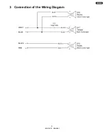
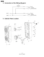
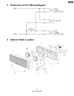
Page 188: ...3 Connection of the Wiring Diagram 4 Cabinet Parts Location 5 service m speaker 11 ...

Page 189: ...Assembly as arrow shown Step 3 Slot a piece of wood chip in between Front Panel and the steel ruler as arrow shown Step 4 Use the screwdriver to slightly lift up Front Panel as arrow shown Note Be careful with the bosses which are glued to Wooden Cabinet Assembly Step 5 Remove Front Panel from Wooden Cabinet Assembly as arrow shown 1 1 1 Assembly of Front Panel 1 1 Disassembly of Front Panel 6 ser...

Page 190: ...Place Front Panel firmly back to Wooden Cabinet Assembly 1 2 Disassembly of Tweeter Follow step 1 to step 5 in item 1 1 Step 1 Detach the black and blue wires from Tweeter Step 2 Remove 4 screws from Tweeter 1 3 Disassembly of Woofer Follow step 1 to step 5 in item 1 1 7 service m speaker ...

Page 191: ...r Step 2 Remove Woofer by detaching the white and blue wires 1 4 Disassembly of Woofer Follow step 1 to step 5 in item 1 1 Step 1 Remove 4 screws from Woofer Step 2 Remove Woofer by detaching the red and black wires 8 service m speaker ...

Page 192: ...3 Connection of the Wiring Diagram 9 service m speaker ...

Page 193: ...4 Cabinet Parts Location 3 10 service m speaker ...

Page 194: ...ACKING WOOFER WOOFER M 5 RMRM0016 BACK CAVITY RMRX0061 K WOOFER SPACER PRINT SPEC SHEET M Ref No Part No Part Name Description Remarks 6 M 7 XTB4 10GFJ A SCREW M 8 XTB4 16AF SCREW M 9 10 RKA0072 KJ LEG CUSHION M PACKING MATERIALS P1 RPNM0167 POLYFOAM M P2 RPFM0029 MIRAMAT M SPEAKER CAPACITOR SP1 EAS6PH126A TWEETER M SP2 EAS12P546A WOOFER M SP3 EAS20PL290A SUPERWOOFER M C1 ECEA1HAY1R8 1 8 UF 50V M ...

Page 195: ...emove Front Panel from Rear Cabinet Assembly as arrow shown 1 2 Disassembly of Tweeter Follow step 1 to step 2 in item 1 1 Step 1 Detach the blue and gray wires from Tweeter Step 2 Remove 4 screws from Tweeter 1 3 Disassembly of Woofer Follow step 1 to step 2 in item 1 1 1 1 Disassembly of Front Panel 12 service m speaker ...

Page 196: ...Step 1 Detach the black and blue wires from Woofer Step 2 Remove 4 screws from Woofer 13 service m speaker ...

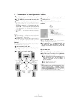
Page 197: ...and corners can result in excessive bass Cover walls and windows with a thick curtain The angles in the diagram are approximate Notes Keep your speakers at least 10 mm away from the system for proper ventilation You cannot take the front net off the speakers Connection Use only the supplied speakers Using other speakers can damage the unit and sound quality will be negatively affected Set the spea...

Page 198: ...3 Connection of the Wiring Diagram 4 Cabinet Parts Location 15 service m speaker ...

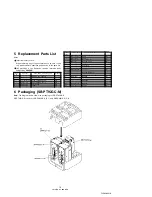
Page 199: ... M 2 RYBX0107 S REAR CABINET ASS Y M 3 RGNX0302 K SPEC SHEET M 4 XTB3 10GFJ SCREW M Ref No Part No Part Name Description Remarks 5 XTB3 12GFJ SCREW M 6 XTB3 8GFJ SCREW M 7 RKA0072 KJ LEG CUSHION M 8 REEX0493 NETWORK ASS Y M CAPACITOR C1 ECEA1HAY1R8 1 8UF 50V M PACKING MATERIAL P1 RPFX0145 MIRAMAT M SPEAKERS SP1 EAST6PH08A6 TWEETER M SP2 L0AA08A00017 WOOFER M 6 Packaging SB PT92GC M Note The diagra...

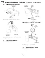
Page 200: ...n 1 2 Disassembly of Woofer 1 Follow step 1 to step 2 in Item 1 1 Step 1 Detach the red and black wires from Woofer 1 Step 2 Remove 4 screws from Woofer 1 1 3 Disassembly of Woofer 2 Follow step 1 to step 2 in Item 1 1 1 Disassembly Process CENTRAL SC TM850 950DIN SC TM900 1000DVD 1 1 Disassembly of Front Panel 17 service m speaker ...

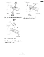
Page 201: ...lack wires from Woofer 2 Step 2 Remove 4 screws from Woofer 2 1 4 Disassembly of Piezo Speaker Follow step 1 to step 2 in Item 1 1 Step 1 Remove the glue from Piezo Speaker Step 2 Disconnect the Piezo Assembly 18 service m speaker ...

Page 202: ... corners can result in excessive bass Cover walls and windows with a thick curtain The angles in the diagram are approximate Notes Keep your speakers at least 10 mm away from the system for proper ventilation You cannot take the front net off the speakers Connection Use only the supplied speakers Using other speakers can damage the unit and sound quality will be negatively affected Set the speaker...

Page 203: ...3 Connection of the Wiring Diagram 4 Cabinet Parts Location 20 service m speaker ...

Page 204: ...M 2 RYBX0105 S REAR CABINET ASS Y M 3 REEX0491 SPEAKER CORD ASS Y M 4 XTB3 10GFJ SCREW M Ref No Part No Part Name Description Remarks 5 RGNX0301 K SPEC SHEET M 6 XTB3 12GFJ SCREW M 7 RASX0004 PIEZZO ASS Y M 8 RKA0072 KJ LEG CUSHION M CAPACITOR C1 ECA1HAY5R6S 5 6uf 50V M PACKING MATERIALS P1 RPNX0334 POLYFOAM M P2 RPFX0146 MIRAMAT M SPEAKER SP1 L0AA08A00018 WOOFER M 6 Packaging SB PT92GC M Note The...

Reviews: