
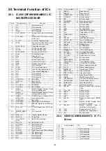
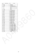
136
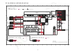
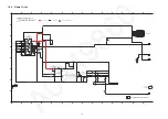
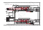
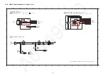
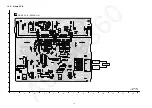
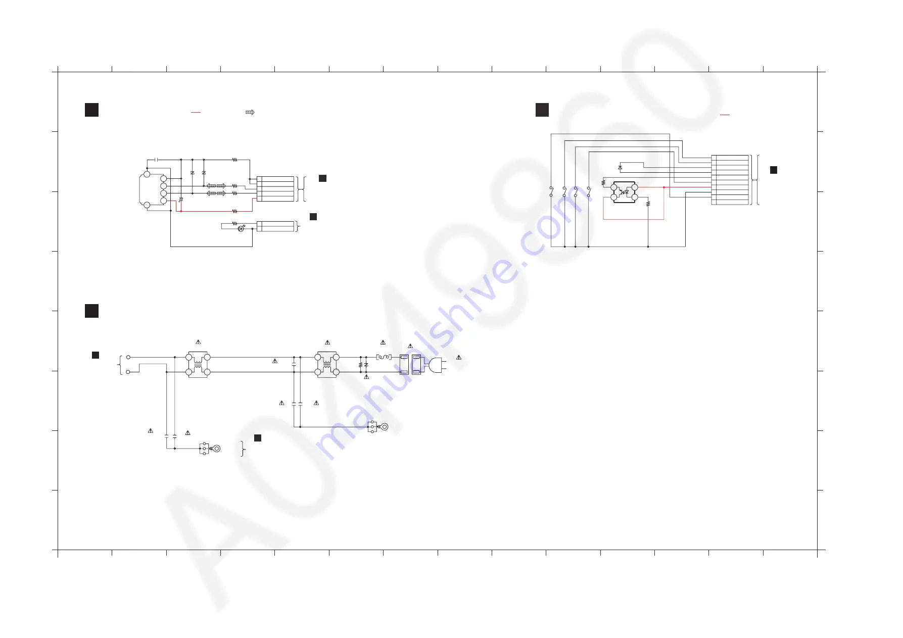
18.8. USB, Deck Mechanism & AC Inlet Circuit
L
L
DECK MECHANISM CIRCUIT
O
AC INLET CIRCUIT
SCHEMATIC DIAGRAM - 18
SA-VK680EE USB / DECK MECHANISM / AC INLET CIRCUIT
N
TO
SMPS CIRCUIT
IN SCHEMATIC
DIAGRAM - 17
A
TO
DVD MODULE CIRCUIT
(FP9001)
IN SCHEMATIC
DIAGRAM - 1
B
TO
MAIN CIRCUIT
(CN2813)
IN SCHEMATIC
DIAGRAM - 7
B
TO
MAIN CIRCUIT
(CN2752)
IN SCHEMATIC
DIAGRAM - 10
1
10
: +B SIGNAL LINE
: USB SIGNAL LINE
: +B SIGNAL LINE
I
TO
MIC CIRCUIT
(ZJ6002*)
IN SCHEMATIC
DIAGRAM - 12
A
B
C
D
E
F
G
H
1
2
3
4
5
6
7
8
9
10
11
12
13
14
1
2
3
4
5
6
7
8
9
10
11
12
13
14
A
B
D
E
F
H
G
C
J
USB CIRCUIT
2
3
4
1
C1110
0.1
2
5
G
1
4
6
G
3
JK1111
2.7K
R1111
2
3
1
5
5
1
4
CN1113
B3AAA0001031
LED
D1111
EZJZ1V171AA
VA1120
EZJZ1V171AA
VA1110
0
LB1200
0
K1200
0
K1210
0
LB1210
6.3V100
C1100
1
2
ZJ1111*
RIPPING LED
LED CONTROL
USB PORT
-D
USB5V
+D
DGND
DGND
DGND
-D
+D
USB5V
C5705
F1BAF1020020
1000P
C5704
F1BAF1020020
1000P
C5706
F1BAF1020020
1000P
C5707
F1BAF1020020
1000P
3
2
1
3
2
1
ZJ5701
ZJ5702
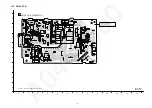
ERZV10V511CS
220 ~ 240V
50Hz
AC IN
2
3
4
1
L5703
ELF22V020A
4.7M
R5701
DZ5701
C5701
0.33
F0CAF334A087
ZA5701
P5701
ZA5702
T5AH 250V
BLK
RED
F1
R952
PHOTO INTERUPTOR
820
6
8
9
7
2
1
4
5
3
10
CN1304
D951
MA2C16500E
R953 39K
S952
S953
S951
3
4
1
2
CNB13030R2AU
IC971
VREF+
PHOTO
VREF-
PL GND
REC SW
PL
MODE AN6
HALF AN7
REVERSE REC INH
NC
HALF
MODE
REC SW
L5701
ELF15N035AN
S954
RECINH_R
Summary of Contents for SA-VK680EE
Page 13: ...13 ...
Page 48: ...48 ...
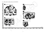
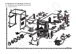
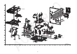
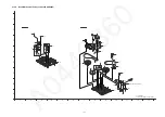
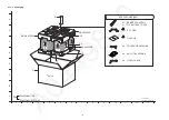
Page 50: ...50 9 2 Main Components and P C B Location ...
Page 116: ...116 ...
Page 118: ...118 ...
Page 144: ...144 ...