background image

© Panasonic Corporation 2013. All rights reserved.
Unauthorized copying and distribution is a violation
of law.

PSG1303046CE

DVD Home Theater Sound System

Model No.

SA-XH201GW

Product Color: (K)...Black Type

TABLE OF CONTENTS

PAGE

PAGE

1 Safety Precautions----------------------------------------------- 3

1.1. General Guidelines---------------------------------------- 3
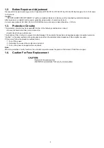
1.2. Before Repair and Adjustment ------------------------- 4
1.3. Protection Circuitry ---------------------------------------- 4
1.4. Caution For Fuse Replacement------------------------ 4
1.5. Safety Part Information----------------------------------- 5

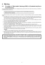
2 Warning -------------------------------------------------------------- 6

2.1. Prevention of Electrostatic Discharge (ESD)

to Electrostatically Sensitive (ES) Devices---------- 6

2.2. Precaution of Laser Diode------------------------------- 7
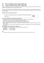
2.3. Service caution based on Legal restrictions -------- 8
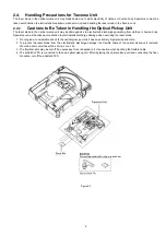
2.4. Handling Precautions for Traverse Unit-------------- 9
2.5. Grounding for electrostatic breakdown

prevention --------------------------------------------------10

3 Service Navigation ----------------------------------------------11

3.1. Service Information -------------------------------------- 11
3.2. Firmware Version-Up Information --------------------12

4 Specifications ---------------------------------------------------- 14

4.1. Others (Licences) ---------------------------------------- 15

5 General/Introduction------------------------------------------- 16

5.1. Power-Saving Features -------------------------------- 16
5.2. Linked Operations with the TV (VIERA Link

“HDAVI Control™”)  ------------------------------------- 17

5.3. Disc Information ------------------------------------------ 19

6 Location of Controls and Components------------------ 21

6.1. Remote Control Key Button Operations------------ 21
6.2. Main Unit Key Button Operations -------------------- 22

7 Installation Instructions -------------------------------------- 23

7.1. Speaker Connections  ---------------------------------- 23
7.2. Radio Antenna connection----------------------------- 23
7.3. Connection with an ARC compatible TV ----------- 24

8 Operating Instructions ---------------------------------------- 25

8.1. Removing of disc during abnormality --------------- 25

9 Service Mode ----------------------------------------------------- 27

Note: Please refer to the original service manual for:

O

O

O

O

 DVD Mechanism Unit, Order No. PSG1201015AE

O

O

O

O

 Speaker system SB-XH201GW-K, Order No. PSG1303047CE

Summary of Contents for SA-XH201

Page 1: ...5 Grounding for electrostatic breakdown prevention 10 3 Service Navigation 11 3 1 Service Information 11 3 2 Firmware Version Up Information 12 4 Specifications 14 4 1 Others Licences 15 5 General Introduction 16 5 1 Power Saving Features 16 5 2 Linked Operations with the TV VIERA Link HDAVI Control 17 5 3 Disc Information 19 6 Location of Controls and Components 21 6 1 Remote Control Key Button O...

Page 2: ...bly of D Amp P C B 56 12 13 Disassembly of AC Inlet P C B and SMPS P C B 57 12 14 Disassembly of DVD Mechanism Unit 59 12 15 Replacement of Traverse unit 60 13 Service Position 65 13 1 Checking of Panel P C B 65 13 2 Checking of Main P C B 65 13 3 Checking of D Amp P C B 66 13 4 Checking of SMPS P C B and AC Inlet P C B 68 14 Block Diagram 69 14 1 Backend 69 14 2 IC Terminal Chart 70 14 3 System C...

Page 3: ...ock hazards 1 1 1 Leakage Current Cold Check 1 Unplug the AC cord and connect a jumper between the two prongs on the plug 2 Measure the resistance value with an ohmmeter between the jumpered AC plug and each exposed metallic cabinet part on the equipment such as screwheads connectors control shafts etc When the exposed metallic part has a return path to the chassis the reading should be between 1M...

Page 4: ...e operated if either of the following conditions are noticed No sound is heard when the power is turned on Sound stops during a performance The function of this circuitry is to prevent circuitry damage if for example the positive and negative speaker connection wires are shorted or if speaker systems with an impedance less than the indicated rated impedance of the amplifier are used If this occurs...

Page 5: ...ET SMPS 10 RGR0428K G REAR PANEL 17 RKM0708 K TOP CABINET 301 RAY1104A V TRAVERSE ASS Y A2 K2CQ2YY00119 AC CORD A3 RQT9809 G O I BOOK En PCB7 REP4761B SMPS P C B RTL PCB8 REP4761B AC INLET P C B RTL DZ5701 ERZV10V511CS ZNR E S D L5701 G0C123M00001 INDUCTOR L5702 G0C123M00001 INDUCTOR T5701 ETS61BA126AD MAIN TRANSFORMER T5751 ETS19AB2E6AG SUB TRANSFORMER PC5702 B3PBA0000579 PHOTO COUPLER PC5720 B3P...

Page 6: ...solder or unsolder ES devices 4 Use only an anti static solder removal device Some solder removal devices not classified as anti static ESD protected can generate electrical charge sufficient to damage ES devices 5 Do not use freon propelled chemicals These can generate electrical charges sufficient to damage ES devices 6 Do not remove a replacement ES device from its protective package until imme...

Page 7: ...ation power from pickup 100 µW VDE Laser radiation from the pickup unit is safety level but be sure the followings 1 Do not disassemble the pickup unit since radiation from exposed laser diode is dangerous 2 Do not adjust the variable resistor on the pickup unit It was already adjusted 3 Do not look at the focus lens using optical instruments 4 Recommend not to look at pickup lens for a long time ...

Page 8: ...is used Definition The letter of PbF is printed on the PCB using the lead free solder To put lead free solder it should be well molten and mixed with the original lead free solder Remove the remaining lead free solder on the PCB cleanly for soldering of the new IC Since the melting point of the lead free solder is higher than that of the normal lead solder it takes the longer time to melt the lead...

Page 9: ...ial care must be taken avoid caution to electrostatic discharge damage when servicing the laser diode 1 Do not give a considerable shock to the optical pickup unit as it has an extremely high precise structure 2 To prevent the laser diode from the electrostatic discharge damage the flexible cable of the optical pickup unit removed should be short circuited with a short pin or a clip 3 The flexible...

Page 10: ...stroyed by the static electricity of the working environ ment 2 5 1 Worktable grounding Put a conductive material sheet or iron sheet on the area where the optical pickup is placed and ground the sheet 2 5 2 Human body grounding Use the anti static wrist strap to discharge the static electricity form your body Figure 2 3 Figure 2 3 ...

Page 11: ...service this model Please place orders using the parts list and not the drawing reference numbers If the circuit is changed or modified this information will be followed by supplement service manual to be filed with original service manual Micro processor 1 The following components are supplied as an assembled part Micro processor IC IC2300 RFKWMXH300GS ...

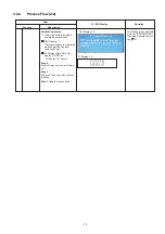
Page 12: ...rk and can t be recovered by CD update again User can put both files into the same root directory DVD MODEL will choose the right ROM files to update its firmware FL GUI Display Remarks Item Description Process 1 2 GUI Display 1 1 Step 1 Power on main unit Step 2 Change selector to DVD CD mode default is CD DVD mode Step 3 Load in the disc with software firmware update data After disc reading GUI ...

Page 13: ...e press and hold main unit OPEN CLOSE then press remote control key 10 Update Completed If firmware software update completes successfully GUI Display 1 3 Firmware update is completed please open the tray and remove the disc GUI Display 1 3 Step 5 Eject the disc and power off main unit Step 6 Power on the unit and do system initialize Step 7 Update process finish ...

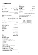
Page 14: ... Bit rate Up to 4 Mbps Xvid ODISC SECTION Discs played 8 cm or 12 cm 1 DVD DVD Video Xvid 4 5 2 DVD R DVD Video MP3 2 4 JPEG 3 4 Xvid 4 5 3 DVD R DL DVD Video Xvid 4 5 4 DVD RW DVD Video MP3 2 4 JPEG 3 4 Xvid 4 5 5 R RW Video 6 R DL Video 7 CD CD R RW CD DA Video CD SVCD 1 MP3 2 4 JPEG 3 4 Xvid 4 5 1 Conforming to IEC62107 2 MPEG 1 Layer 3 MPEG 2 Layer 3 MPEG 2 5 Layer 3 3 Exif Ver 2 1 JPEG Baseli...

Page 15: ...15 4 1 Others Licences ...

Page 16: ...16 5 General Introduction 5 1 Power Saving Features ...

Page 17: ...17 5 2 Linked Operations with the TV VIERA Link HDAVI Control ...

Page 18: ...18 5 2 1 Easy Control With Viera Remote Control ...

Page 19: ...19 5 3 Disc Information 5 3 1 Media that can be played ...

Page 20: ...20 5 3 2 File Extension Type Support MP3 JPEG Xvid ...

Page 21: ...21 6 Location of Controls and Components 6 1 Remote Control Key Button Operations ...

Page 22: ...22 6 2 Main Unit Key Button Operations ...

Page 23: ...ions Turn off all equipment before connection and read the appropriate operating instructions Do not connect the AC power supply cord until all other connections are completed 7 1 Speaker Connections 7 2 Radio Antenna connection ...

Page 24: ...24 7 3 Connection with an ARC compatible TV ...

Page 25: ...he power cannot be turned off 1 Press hold the POWER button to turn off the power forcibly then press hold SKIP FWD button on remote and OPEN CLOSE button on main unit for 5 seconds 8 1 2 When the Forcible Disc Eject cannot be done 1 Turn off the power and remove AC cord 2 Insert Paper Clip into the hole on the bottom of unit and slide the Paper Clip on the direction of the arrow to eject tray sli...

Page 26: ...26 3 Gently pull out the tray Refer to Figure 8 2 Caution If the tray is not able to move do not use force as it may damage the gears drive mechanism 4 Remove the disc Figure 8 2 ...

Page 27: ... cord while button being pressed FL Display will show _ _ _ _ _ _ _ _ 4 Release button 9 2 Panel Code Setting Operation 9 2 1 Checking of Panel Code 1 In STOP no disc mode press OPEN CLOSE button on main unit and 6 button on the remote control unit FL Display Figure 9 1 Display is automatically clear after 5 seconds Note Refer to Figure 9 2 for Video Design Information ...

Page 28: ...hinese GW 5 5PP India English English GT English NA Traditional Chinese 3 PAL NTSC NTSC E 3PN Taiwan Traditional Chinese English English English GK English NA Simplified Chinese 6 6PN China Simplified Chinese Japanese English NA Spanish Panama French Brazilian Portuguese PN 4 NTSC Central S America Brazil Spanish 4PN English NA Spanish Panama French Brazilian Portuguese PB 4 NTSC NTSC Central S Am...

Page 29: ...ew panel code using remote control refer to Figure 9 3 Step4 Press OK on remote control Step5 Unplug AC power cord Step6 Plug AC power cord Step7 Press button on main unit Step8 Check panel code refer to section 9 2 1 Figure 9 3 Main P C B Part No REP4923A REP4923D REP4943A REP4943B Default Code 661 870 261 422 Support Model Panel Code XH60GA 360 XH60GS 370 XH60PH XH60GW 380 361 XH100GA 260 XH100G...

Page 30: ...al notation to one place of decimal Focus drive value is shown in hexadecimal notation Display 1 Jitter rate Jitter check mode Display 2 Lead Error Counter Focus Drive Value Press to exit In STOP with disc inside tray mode press OPEN CLOSE button on the main unit and 5 button on the remote control unit Press FL Display on remote control unit for next page FL Display Error code check Error code che...

Page 31: ... button on the main unit and FUNCTIONS button on the remote control unit To exit press OPEN CLOSE button on the main unit and CANCEL button on the remote control unit To exit press OPEN CLOSE button on the main unit and CANCEL button on the remote control unit The value denotes the current in decimal notation DVD laser current measurement mode DVD laser drive current measurement For DVD laser driv...

Page 32: ...ROM IC FL Display sequence Display 1 2 In STOP no disc mode press OPEN CLOSE button on the main unit and 10 button on the remote control unit Cancelled automatically 5 seconds later In STOP no disc mode press OPEN CLOSE button on the main unit and 7 button on the remote control unit Press FL Display button on remote control unit for next page FL Display If the version of the EEPROM does not match ...

Page 33: ...TOP no disc mode press OPEN CLOSE button on the main unit and button on the remote control unit Timer 1 reset Timer 2 check Timer 2 reset Timer 1 check Laser operation timer is measured separately for DVD laser and CD laser FL Display sequence Display 1 2 Timer 1 reset Laser operation timer of both DVD laser and CD laser is reset all at once Timer 2 check Spindle motor operation timer Timer 2 rese...

Page 34: ...ple Self Diagnostic Mode To enter into self diagnostic checking Press hold OPEN CLOSE on main unit follow by 4 then 9 on remote control When no disc in tray System will clear all of the contents of unusual error code from the memory In self diagnostic mode press OPEN CLOSE on remote control To exit press on main unit or remote control In self diagnostic mode press CANCEL on remote control To exit ...

Page 35: ...tabilized power supply In normal operation when DCDET1 is detected L Low for two consecutive times F76 is displayed on FL for 1 seconds and after that PCONT will be turned to L Low Press OPEN CLOSE on main unit for next error Diagnosis Contents Description of error Automatic FL Display Remarks IPOD OVER CURRENT Over current occurs in Power Supply for iPod charging Disc Region In normal operation w...

Page 36: ...pyright protection technology Digital image signal encryption scheme Press OPEN CLOSE on main unit for next error Press OPEN CLOSE on main unit for next error Press OPEN CLOSE on main unit for next error Press OPEN CLOSE on main unit for next error Press OPEN CLOSE on main unit for next error U703 HDMI DVI authentication error When authentication HDCP with the TV side fails when connecting it with...

Page 37: ...in unit displays LOCKED while the lock function mode is entered Prohibiting operation of selector and disc 1 Select the DVD CD function 2 Power on the main unit 3 Press and hold down OPEN CLOSE button and VOL button on the main unit for three seconds or more LOCKED appears when the function is activated Note The following buttons are invalid and the main unit displays LOCKED while the lock functio...

Page 38: ...ON working normally for sometime then F61 Condition 2 With Stanby LED Off or flickering 3 F1 Fuse open 3 Fuse F1 1 DC DC circuit 1 Thermal Diode D5802 2 SMPS FFC loose 3 LDO regulator 4 Photocoupler PC5720 1 Transformer T5701 2 Photocoupler PC5720 1a Pin 11 12 shorted to pin 13 14 1b Pin 16 shorted to pin 17 1a L2902 Open no input to IC2901 1b Faulty IC2901 no output voltage at pin 10 and 11 1a Im...

Page 39: ...39 10 1 1 SMPS P C B Figure 10 1 SMPS P C B Photocoupler PC5702 PC5799 Switching IC IC5799 Switching IC IC5701 Transformer T5701 Photocoupler PC5720 Thermal Diode D5802 ...

Page 40: ...40 10 1 2 Main P C B Figure 10 2 Main P C B IC2901 L2902 Q2904 R2399 CL8530 CL8531 CL8532 LB2761 Side B of Main P C B Side A of Main P C B Q2902 R8556 R8556 Q2903 L2908 ...

Page 41: ...ltage across R8566 which has a resistance value of 4 7 ohm 2 Calculate the CD Laser current by the following formula CD_LD VCD 4 7 1 Measurement the voltage VDVD on the testpoints CL8530 CL8532 This is voltage across R8556 which has a resistance value of 4 7 ohm 2 Calculate the DVD Laser current by the following formula DVD_LD VCD 4 7 Refer to 10 1 2 Main P C B Figure 10 2 Main P C B Refer to 10 1...

Page 42: ...93 94 95 IC8251 Pin 11 to 18 Check for solder short and or component missing damaged a Check connection from Main to Traverse unit FP8251 3 Disc not spinning 4 Traverse not moving 5 Traverse and spindle abnormal movement b Check motor driver circuitry on the voltages and control signals IC8251 Check for solder short and or component damaged 6 Cannot read the disc but spindle motor is spinning Cann...

Page 43: ... HDMI Transmitter DVD Decorder IC8001 1 8 V Supply 8 Hot Plug Signal 9 HDMI Interface Reference Resistor 1 Supply to HDMI transmitter intergrated IC8001 2 Check for Capacitor short to GND Check Digital Signal Data communication lines from IC8001 to Serial Flash IC IC8651 Check the setting under SETUP menu if HDMI Audio Output option is turned ON Clock TXCP TXCN Pin 10 12 Data TXD0P TXD0N Pin 7 9 D...

Page 44: ...44 11 Service Fixture Tools Prepare service tools before process service position Ref No Service Tools Remarks SFT1 Main P C B CN2006 D Amp P C B CN5402 RFKZBTT270K3 18P FFC ...

Page 45: ...ture after prolong use See caution as described below During disassembly and assembly please ensure proper service tools equipments or jigs is being used During replacement of component parts please refer to the section of Replacement Parts List as described in the ser vice manual Select items from the following indexes when disassembly or replacement are required Disassembly of Top Cabinet Replac...

Page 46: ...2 9 Rear Panel 12 13 AC Inlet P C B and SMPS P C B 12 11 Main P C B 12 12 D Amp P C B 12 6 Front Panel Block 12 8 Panel P C B 12 4 Top Cabinet 12 7 Operation Button P C B and Power Button P C B 12 10 Fan Unit 12 14 DVD Mechanism Unit 12 15 Traverse Unit ...

Page 47: ...47 12 3 Main Components and P C B Locations ...

Page 48: ...ly of Top Cabinet Step 1 Remove 2 screws Step 2 Remove 5 screws Step 3 Slightly release both sides of the Top Cabinet as dia gram shown Step 4 Slightly lift both sides of the Top Cabinet in an upward direction about 30 ...

Page 49: ...Top Cabinet Caution During assembling ensure that the Top Cabinet is inserted into the Front Panel Block 12 5 Replacement of Tray Ornament 12 5 1 Disassembly of Tray Ornament Step 1 Use a Paper Clip and insert into the hole at the bottom of the unit Step 2 Push the Paper Clip sideway in the direction of the arrow to eject the Tray Step 3 Slide the Tray out as direction of arrow ...

Page 50: ...e Tray Step 5 Remove the Tray Ornament in the direction of arrow 12 5 2 Assembly of Tray Ornament Step 1 Align the guide rib of Tray Ornament with the Tray Step 2 Insert the Tray Ornament into the Tray Caution Ensure that the Tray Ornament is fully catched onto the Tray Step 3 Slide the Tray until it is fully closed ...

Page 51: ... connector CN6001 on Panel P C B Step 2 Release tabs on both sides of the Front Panel Block in the direction of arrow Step 3 Release tabs at the bottom of the unit Caution Do not exert strong force when releasing the tabs Caution During assembling ensure that the Front Panel Block is properly inserted and fully catched onto the Bot tom Chassis ...

Page 52: ...assembly of Top Cabinet Refer to Disassembly of Tray Ornament Refer to Disassembly of Front Panel Block Step 1 Remove 2 screws Step 2 Lift up the Operation Button P C B Caution During assembling ensure that the Operation Button P C B is properly located and fully seated onto the Front Panel Block Step 3 Remove 1 screw ...

Page 53: ... Button P C B is properly located and fully seated onto the Front Panel Block 12 8 Disassembly of Panel P C B Refer to Disassembly of Top Cabinet Refer to Disassembly of Tray Ornament Refer to Disassembly of Front Panel Block Step 1 Detach 21P FFC at the connector P6001 on Panel P C B Step 2 Remove 2 screws Step 3 Remove the Panel P C B Caution During assembling ensure that the Panel P C B is prop...

Page 54: ...bs at each side of the Rear Panel in the direction of arrow Step 3 Remove the Rear Panel 12 10 Disassembly of Fan Unit Refer to Disassembly of Top Cabinet Step 1 Lift up the Wire Clamper Step 2 Detach the 3P Fan Wire at connector CN5401 on D Amp P C B Step 3 Remove 2 screws Step 4 Lift up to remove the Fan Unit ...

Page 55: ...bs at each side of the Rear Panel in the direction of arrow Step 3 Detach 18P FFC at the connector CN2006 on Main P C B Step 4 Detach 10P FFC at the connector CN2004 on Main P C B Step 5 Detach 21P FFC at the connector CN2002 on Main P C B Step 6 Detach 5P FFC at the connector FP8252 on Main P C B Step 7 Detach 6P FFC at the connector FP8251 on Main P C B Step 8 Detach 24P FFC at the connector FP8...

Page 56: ...mbly of D Amp P C B Refer to Disassembly of Top Cabinet Step 1 Remove 7 screws Step 2 Release tabs at each side of the Rear Panel in the direction of arrow Step 3 Lift up the Wire Clamper Step 4 Detach 3P Fan Wire at the connector CN5401 on D Amp P C B Step 5 Detach 18P FFC at the connector CN5402 on D Amp P C B Step 6 Detach 4P Cable at the connector CN5400 on D Amp P C B ...

Page 57: ...ing assembling ensure that the D Amp P C B is properly located seated onto the Bottom Chassis 12 13 Disassembly of AC Inlet P C B and SMPS P C B Refer to Disassembly of Top Cabinet Step 1 Remove 1 screw Step 2 Remove 2 screws Step 3 Lift up to remove the AC Inlet P C B ...

Page 58: ...is Step 4 Detach 10P FFC at the connector CN5700 on SMPS P C B Step 5 Detach 4P Cable at the connector CN5400 on D Amp P C B Step 6 Remove 4 screws Step 7 Lift up to remove the SMPS P C B and AC Inlet P C B Caution During assembling ensure that the SMPS P C B is properly located seated onto the Bottom Chassis ...

Page 59: ...h 6P FFC at the connector FP8251 on Main P C B Step 3 Detach 24P FFC at the connector FP8531 on Main P C B Step 4 Remove 4 screws Step 5 Slightly lift up to remove the DVD Mechanism Unit from the unit Caution During assembling ensure that the DVD Mecha nism Unit is properly located seated on the bottom chas sis before screwing Step 6 Attach a short pin to the 24P FFC of the DVD Mecha nism ...

Page 60: ...up unit Note 1 When the optical pickup unit is defective the overall traverse unit needs replacement 2 Please note that appropriate actions need to be taken to prevent static damage 12 15 1 Disassembly of Traverse unit Step 1 Use a pin to slide the Traverse Slide Plate until it comes to a stop Step 2 Slide the tray out fully Step 3 Press inwards to release the catches remove the tray ...

Page 61: ...ide the Traverse Slide Plate to the end Step 5 Release the 24P FFC from the slot Step 6 Lift up the Traverse Unit by approximately 45 Step 7 Remove the traverse unit as arrow shown Caution Avoid touching the surface of the OPU on the traverse unit ...

Page 62: ...12 15 2 Assembly of Traverse Unit Step 1 Press release the guide as shown slide the Traverse Slide Plate to the end Step 2 Insert the Traverse unit at approximately 45 into the DVD Mechanism as arrow shown ...

Page 63: ...tep 4 Slide the Traverse Slide Plate to lock the Traverse Unit as shown Step 5 Insert the 24P FFC into the slot Caution Ensure that the 24P FFC are properly inserted into the slots as shown Step 6 Slide the Traverse Slide Plate until it stop at the Guide ...

Page 64: ...Align the grooves of the tray with the guides of the mechanism Step 8 Insert the Tray Step 9 Align the guides of the Traverse Slide Plate with the grooves when sliding the tray in Step 10 Slide the tray in fully ...

Page 65: ...k Step 4 Remove 2 screws Step 5 Place the Front Panel Block on the insulated material as diagram shown Step 6 Connect 4P Cable at the connector CN6001 on Panel P C B Step 7 Upset the Panel P C B and place it on an insulated material Step 8 Proceed to check the Panel P C B 13 2 Checking of Main P C B 13 2 1 Checking of Main P C B Side B Step 1 Remove Top Cabinet Step 2 Proceed to check Side B of Ma...

Page 66: ...p 4 Remove 4 screws Step 5 Connect 18P Extension FFC RFKZBTT270K3 from CN2006 to CN5402 Step 6 Upset the Main P C B and place it onto the insulated material Step 7 Proceed to check Side A of Main P C B 13 3 Checking of D Amp P C B Step 1 Remove Top Cabinet Step 2 Remove D Amp P C B Step 3 Place D Amp P C B on an insulated material Step 4 Remove 4 screws ...

Page 67: ...Wire at the connector CN5401 on D Amp P C B Step 7 Connect 18P FFC at the connector CN5402 on D Amp P C B Step 8 Connect 4P Cable at the connector CN5400 on D Amp P C B Step 9 Upset the D Amp P C B and place it on an insulated material Step 10 Proceed to check Side A of D Amp P C B ...

Page 68: ...lector P C B AC Inlet P C B and SMPS P C B Step 3 Connect 10P FFC at the Connector CN5700 on SMPS P C B Step 4 Connect 4P Cable at the Connector CN5400 on D Amp P C B Step 5 Upset the AC Inlet P C B and SMPS P C B and placed onto the insulated material Step 6 Proceed to check AC Inlet P C B and SMPS P C B ...

Page 69: ... RF D 17 FP8531 RF RFIN P CD MD 85 7 FP8531 VR DVD CD MD DVD MD 86 8 FP8531 VR CD DVD MD CD LD SF CLK 5 SI SF DO 2 SO SF DI DVD LD 3 FP8251 INNER SW 3 FP8252 OPEN SW 5 FP8252 CLOSE SW 14 FP8531 F RF F VINSL 4 TRV DRV 95 TRV DRV VINLD 23 FWD 6 REV 7 SPN DRV 94 SPN DRV VINTK 26 TRK DRV 93 TRK DRV VINFC 1 FOC DRV 90 FOC DRV MUTE 28 GPIO39 97 DRVSB 16 VOTK 21 FP8531 T 14 VOFC 23 FP8531 F 6 FP8531 CD L...

Page 70: ...Q7 DQ8 DQ9 DQ10 DQ11 DQ12 DQ13 DQ14 DQ15 53 IC8051 64M SDRAM IC8001 DVD DECODER TXD0P 52 TXD0 7 D0 TXD0N 51 TXD0 9 D0 TXD1P 54 TXD1 4 D1 TXD1N 53 TXD1 6 D1 TXD2P 56 TXD2 1 D2 TXD2N 55 TXD2 3 D2 IC8001 DVD DECODER P3901 HDMI AV OUT ARC SIGNAL NAME TC 3 PIN NO PORT NAME PIN NO PORT NAME SIGNAL NAME TC 1 PIN NO PORT NAME PIN NO PORT NAME 125 MA 0 23 123 MA 1 24 126 MA 2 25 127 MA 3 26 122 MA 4 29 124...

Page 71: ...W CLOSE SW 1 CLOSE SW CLOSE SW MICROP RX 27 MICRO P TX MICRO P TX VOLUME S6006 VOLUME S6004 DAP RST 79 DAP RST DAP MUTE 32 DAP MUTE DAP RST DAP MUTE FAN DA 2 FAN DA FAN DA PCONT 48 PCONT PCONT FWD 36 FWD REV 37 REV FWD SPDIF SW 99 SPDIF SW SPDIF SW AMUTE 38 AMUTE AMUTE MICROP TX 28 MIRCO P RX MICRO P RX REV DAP SCK TUN RST 21 TUN REST TUN REST DAP SDA CEC IN OUT 15 CEC IN OUT CEC IN OUT TUN INT TU...

Page 72: ...006 DAP SCL SCL 25 4 15 CN5402 CN2006 RESET RESET 11 1 18 CN5402 CN2006 MUTE SDIN3 DAP SCL RESET MUTE MUTE 14 2 17 CN5402 CN2006 FAN DA DAP MUTE DAP RST DC DET2 FAN AD FAN DA FAN DA 16 3 CN5402 CN2006 1 CN5401 3 CN5401 DCDET 16 FAULT 14 INPUT C 15 INPUT D 4 RESET DIGITAL AMPLIFIER C1AB00003986 IC5100 5 INPUT A 6 INPUT B SURROUND LEFT OUT A BST A OUT B BST B 11 JK5001 12 JK5001 40 OUT A 39 44 35 43...

Page 73: ...ORMER T5751 MAIN TRANSFORMER T5701 PC5799 FEEDBACK PC5702 SYNC PC5901 PCONT DC DETECT SHUNT REGULATOR C0DAZYY00039 IC5801 FEEDBACK CIRCUIT PC5720 FEEDBACK D5712 D5703 D5707 F1 DZ5701 L5702 1 4 2 3 L5701 1 4 2 3 RED RED TL31 TL30 BLK BLK TL21 TL20 NOTE REF IS FOR INDICATION ONLY 3 K VREF 4 FB 2 VDD 1 D 5 5 VCC 4 CL 3 6 3 4 2 1 3 1 2 7 4 5 1 2 11 16 10 12 14 17 13 8 6 7 9 TH5702 D5701 D5896 D5716 D5...

Page 74: ...R3V VDD SDRAM VDDDAC VDDP HDMI VDD APE PW D 5V 5 EN 1 8V 2 VCC 1 8V VOLTAGE SUPPLY REGULATOR C0DBEYY00215 IC8111 1 8V ADJ 4 5 PW VDD1R8V PW VDD1R8V 3 3V PW VREF PW SYS3R3V 5V PW A 5V PW D 5V 3 3V PW 3 3V 1 CTL 4 VIN 3 3V VOLTAGE REGULATOR C0DBFYY00166 IC2091 VOUT 5 PW 3 3V 1 CE PW VREF PW SYS3R3V PW 3 3VREF PW VBUS PW 12V 3 3V PW A 5V PW D 5V PW 9V PW M 9V PANEL P C B MAIN P C B 5 6 16 17 P6001 CN...

Page 75: ...V 50Hz AC IN AC INLET P C B SOLDER SIDE PbF RED TL30 BLK TL20 G T5751 SUB TRANSFORMER T5701 MAIN TRANSFORMER 2 1 9 10 2 1 9 10 10 7 8 9 1 2 3 4 5 6 1 4 SMPS P C B SOLDER SIDE PbF CN5700 H5700 BLK TL21 RED TL31 18 17 16 15 14 13 12 11 9 8 7 6 5 4 2 1 F MAIN P C B SIDE B CN2002 CN2004 P3901 FP8252 FP8251 FP8531 TO TRAVERSE PCB DVD MECHANISM UNIT BRS11D TO LOADING PCB DVD MECHANISM UNIT BRS11D CN2006...

Page 76: ...76 ...

Page 77: ... AC rated voltage Capacitors the part no and val ues will be indicated in the Schematic Diagram AC rated voltage capacitors C5700 C5701 C5702 C5704 C5705 C5706 Resistor Unit of resistance is OHM Ω K 1 000 M 1 000 000 Capacitor Unit of capacitance is µF unless otherwise noted F Farads pF pico Farad Coil Unit of inductance is H unless otherwise noted REF is for indication only Voltage and signal lin...

Page 78: ...78 ...

Page 79: ...GNAL LINE CD DVD VIDEO INPUT SIGNAL LINE B SIGNAL LINE VIDEO OUTPUT SIGNAL LINE HD MAIN HDMI SCHEMATIC DIAGRAM 1 6 MI MAIN MICON SCHEMATIC DIAGRAM 7 11 SA XH201GW MAIN HDMI CIRCUIT 2 6 3 6 5 6 1 6 4 6 6 6 USB_DN USB_DP R8322 75 LB8317 0 3 1 2 D8301 DA3X101F0L CVBS_C VGND OPTICAL DIGITAL AUDIO IN R9001 0 R9002 0 L8001 G1C100M00049 2 3 1 JK8001 R8025 0 C8030 6 3V33 PW_D 3R3V OPT_IN VCC GND OPT IN VD...

Page 80: ...100 6 7 5 2 4 3 8 1 C0JBAR000433 2CH MULTIPLEXER IC3954 1 C3968 2K R3905 4 7K R3906 R3907 2K 4 7K R3904 S D G Q3902 FK3503010L S D G Q3903 FK3503010L DDC CLOCK SWITCH DDC DATA SWITCH 0 01 C3955 K3904 0 10K R3947 3 1 2 4 5 IC3952 C0CBCDC00063 5V VOLTAGE REGULATOR C3954 0 1 1 C3956 OPT_IN B Y 1Y A ST VCC GND 2Y Y SELECT 1A 2A VCC GND IN OUT GND VC NOISE BYPASS GPIO34 PW_M 9V 0 01 C3945 LB3906 J0JCC0...

Page 81: ...88 90 IC8001 C1AB00003476 DVD DECODER H0J270500131 X8621 C8621 10P C8622 8P R8569 1K 1000P C8024 RESET J0JHC0000045 LB9001 GND TRV_PWM SPN_PWM TRK_PWM FOC_PWM 8 6 5 7 4 2 2 1 3 D1H88204A043 RX8012 8 6 5 7 4 1 3 D1H88204A043 RX8019 8 6 5 7 4 1 3 D1H88204A043 RX8018 8 6 5 7 4 2 2 2 2 2 2 2 1 3 D1H88204A043 RX8013 8 6 5 7 4 1 3 D1H88204A043 RX8015 8 6 5 7 4 1 3 D1H88204A043 RX8011 22 R8011 8 6 5 7 4 ...

Page 82: ...CC CTL GND K8252 0 4 3 5 1 2 FP8252 LB8012 0 2 4 3 1 6 5 FP8251 TO TRAVERSE P C B DVD MECHANISM UNIT BRS11D TO LOADING P C B DVD MECHANISM UNIT BRS11D R8267 1K 0 1 C8264 R8266 1K R8268 33K FOC_DRV GND PW_D 3R3V 6 19K R8258 1K R8265 R8263 4 7K 0 1 C8256 2 1 27 5 4 24 25 22 17 19 18 15 16 30 20 21 7 11 10 13 14 12 8 29 9 23 6 3 26 28 C0GBY0000117 5CH MOTOR DRIVER IC8251 C8252 16V47 R8262 10K R8261 1...

Page 83: ... FP8531 TO OPTICAL PICKUP UNIT DVD MECHANISM UNIT BRS11D RF_A RF_B R8537 0 RF_F LB8530 J0JHC0000045 R8536 3 3K RF_D RF_C PW_A 5V B1ABDF000026 DVD SELECTOR SWITCH Q8565 R8534 10K RFIN_P R8535 47K RF_E VC LB8532 J0JDC0000102 CD_MD GND R8538 0 LB8531 22 R8570 56 R8572 56 R8573 56 R8571 56 DVD_MD LB8551 J0JDC0000102 LB8561 J0JDC0000102 T T D d C c F F F F T T NC NC MD F E NC B b VCC CD LD RF A a PD GN...

Page 84: ... 10 7 6 8 9 11 2 1 4 3 5 34 36 39 41 42 40 38 49 52 51 54 53 50 44 43 45 47 48 46 37 35 23 22 32 33 IC8051 C3ABPY000070 64M SDRAM DQ11 DQ4 DQ12 DQ3 A7 A5 A6 NC DQ8 VSS DQ9 CLK CKE NC A8 A9 A11 VSS A4 DQ5 DQ10 UDQM A1 A2 WE LDQM RAS CAS VDD A0 CSO A10 AP CS RAMBA0 A3 VDD VDDQ DQ6 DQ7 VSSQ VSSQ VDDQ VSS VSSQ VDDQ DQ15 VDD DQ0 DQ2 DQ13 VSSQ VDDQ DQ14 DQ1 C8606 0 1 3 1 2 4 5 C0EBE0000504 RESET IC8606 ...

Page 85: ... 75 10 8 7 9 12 11 99 100 95 94 96 97 90 91 89 93 92 98 4 6 5 2 1 3 81 82 80 86 87 88 84 83 85 45 19 17 15 14 16 18 43 23 21 20 22 41 24 39 37 33 35 34 29 30 27 26 28 32 31 36 38 25 40 42 44 13 46 IC2300 RFKWMXH300GS MICROPROCESSOR 150K R2315 KEY1 R2395 100 R2346 10K R2355 10K R2354 10K 0 1 C2321 DAP_RST R2385 100 R2384 100 R2339 10K R2338 10K C2306 0 1 0 K2713 PW_SYS3R3V LB2301 J0JBC0000015 DGND ...

Page 86: ...N SDATA3 SRCK SDATA1 SDATA2 CEC_IN_OUT MCLK SPDIF_SW PW_VREF CEC_IN_OUT MCLK SPDIF_SW LRCK SDATA2 SDATA1 SDATA0 SRCK C2100 0 1 AMUTE AMUTE PW_D 5V C2106 0 1 ZJ2004 CHASSIS GROUND 0 1 C2109 HD HD HD GND HD HD HD HD HD HD HD HD HD HD HD HD HD HD HD HD HD HD HD HD D D HD HD PW_D 5V HD FLD_CLK RMT FLD_DAT FLD_STB USB_D USB_D KEY2 PW_VBUS KEY1 LB2760 LB2762 J0JBC0000014 R2399 3 3 J0JBC0000014 LEDCONT C...

Page 87: ...929 C2976 0 015 R2921 39K 0 01 C2962 C2917 0 01 K2703 0 0 L2700 PW_D 5V C2704 6 3V220 R2908 10K 0 1 C2971 PW_M 9V MGND PGND GND R2927 10K 0 22 C2972 R2918 3 3K R2917 3 3K C2981 1000P R2935 0 C2911 680P 0 1 C2964 C2953 0 1 C2973 1200P 8 9 7 6 1 2 5 3 4 12 14 16 18 19 20 17 15 13 10 11 C0DBAYY00729 IC2901 K2905 0 Q2904 B1BACD000018 9V VOLTAGE REGULATOR C2908 10V120 C2909 0 1 1 C2905 0 K2705 0 K2700 ...

Page 88: ... 4 7K TUN_GPIO TUN_REST R57 1K R56 220 0 1 C62 R55 220 AINL LRCK I2S_IN R52 560 C51 1000P G1CR18JA0020 L51 AINR ADGND R66 18K R64 18K R65 10K R67 10K 3P C67 J0JYC0000118 LB52 G2 G3 G1 JK51 R51 2 2K TUN_SCLK TUN_SDIO 0 1 C61 VA51 EZAEG2A50AX C68 0 022 R69 0 R63 0 C63 6P LB51 J0JBC0000032 4 12 1 2 14 T1 17 19 18 16 15 20 3 13 THERMAL PAD 5 11 10 7 6 9 8 IC52 SRCK 33P C66 R60 2 2K R59 2 2K VUEALLPT05...

Page 89: ...C2806 1 R2822 0 R2823 0 0 R2818 0 R2819 ADGND 10K R2870 10K R2871 100P C2872 C2873 1000P 1 5 4 3 2 JK2800 220P C2871 220P C2870 J0JCC0000308 R2874 C2874 220P R2872 10K R2873 10K C2875 220P VGND AUXR VIDEO_OUT AUXL PCONT PW_ 18V SYNC 10K R2741 ECO_CTL 6 8 9 7 2 1 4 5 3 10 CN2004 R2094 0 C2108 0 PW_ 3 3V GND DSP_SCK FAN_DA DSP_I2S_OUT1 DC_DET2 FAN_AD DGND DSP_MCLK_OUT DSP_BCK_OUT SDATA3 DSP_I2S_OUT2...

Page 90: ...01 C6105 10 B0JCMD000010 D6100 5 3 4 8 7 6 2 1 9 T6100 G4D1A0000142 6 3V220 C6103 P11 P10 P2 P4 P6 P8 P7 P5 P3 P1 P9 1K R6012 R6010 68 68 R6011 100P C6013 100P C6014 100P C6012 P12 P14 P13 C6015 1 C6019 0 1 G3 G5 G7 G8 G9 G9 G6 G4 G8 G9 G6 G4 G2 G3 G5 G7 G1 G2 G1 P2 P1 P4 P6 P8 P9 P7 P5 P3 P15 P13 P11 P10 P12 P14 P16 P15 P16 R6015 56K 21 5 6 3 1 2 4 19 9 7 8 16 17 11 10 12 15 14 13 18 20 35 37 42 ...

Page 91: ...G AC INLET CIRCUIT F TO SMPS CIRCUIT IN SCHEMATIC DIAGRAM 19 NOTE REF IS FOR INDICATION ONLY R6021 18K S6004 R6020 1 2K S6006 S6804 R6025 1 2K 2 1 4 3 H6002 1 3 2 H6003 LED DGND KEY 2 LED DGND VOLUME VOLUME OPEN CLOSE KEY 1 KEY 1 S6801 0 L6804 L6806 0 1 3 2 H6001 POWER LED DGND KEY 1 P5701 ZA5701 ZA5702 ERZVA5Z471 DZ5701 3 2 1 ZJ5701 R5701 1 5M TL20 R5700 1 5M TL30 3 2 4 1 L5702 G0C123M00001 F0CAF...

Page 92: ...0 61 59 64 53 50 49 52 51 55 56 54 8 7 9 4 6 5 23 24 21 18 19 17 17 VR_DPLL 18 OSC_CAP 20 22 16 12 13 10 11 15 14 2 3 31 29 30 32 27 28 25 26 IC5301 C1AB00003610 DIGITAL AUDIO PWM PROCESSOR 8 6 5 7 4 2 1 3 D1H83314A042 RX5371 9 7 5 2 3 1 4 6 8 17 15 13 10 12 11 14 16 18 CN5402 47P C5367 47P C5366 10P C5365 10P C5364 C5363 0 1 1M R5353 X5351 H0J135000003 DAP_SCL DAP_SDIN2 DAP_SDIN4 DAP_SDIN3 DAP_SD...

Page 93: ... 3 1 G0C100M00007 L5301 R5317 100K R5316 100K R5314 100K R5315 100K PVDD SD VDD GND R5302 24K PWM_SW PWM_SW 1 C5313 C5314 1 R5303 24K C5318 0 033 3 3 R5301 3 3 R5300 0 1 C5301 C5302 10 0 1 C5300 R5304 C5306 C5303 C5305 0 1 C5304 C5316 1 C5315 1 PWM_C PWM_C VALID PW_ 12 3 3 R5305 C5307 0 1 L5403 G1C4R7MA0172 IC5300 C1AB00003986 0 033 C5312 0 033 C5311 DGND 1 47K 100P 1 DIGITAL AMPLIFIER 43 11 9 10 ...

Page 94: ... CLAMPER ZJ2 1 C5419 2 1 4 3 CN5400 C5418 6 3V100 J0JKB0000003 L5402 560K R5435 B1GBCFNN0038 FAN LOCK DETECT Q5403 R5422 10K R5424 470 10 C5420 27K R5430 R5427 47K PW_ 12V C5140 50V820 C5117 50V820 L5404 G1C4R7MA0172 D5407 DA2J10100L 1 C5425 R5438 100K R5437 4 7K B1ADCE000012 DC DETECT DC DETECT Q5413 B1ABCF000231 Q5412 FAN_DA 6 7 5 2 4 3 8 1 IC5401 C0ABBA000168 DUAL OP AMP R5429 10K R5436 22K R54...

Page 95: ...00 0 033 C5219 C5218 0 033 3 3 R5201 3 3 R5200 0 1 C5201 C5202 10 0 1 C5200 R5204 C5206 C5203 C5205 0 1 C5204 C5216 1 C5215 1 PWM_FL PWM_FL VALID 3 3 R5205 C5207 0 1 IC5200 C1AB00003986 0 033 C5212 0 033 C5211 DGND SD 1 4 7K 100P 1 R5102 24K PWM_SR PWM_SR 1 C5113 C5114 1 R5103 100 0 033 C5119 C5118 0 033 3 3 R5101 3 3 R5100 0 1 C5101 C5102 10 0 1 C5100 R5104 C5106 C5103 C5105 0 1 C5104 C5116 1 C51...

Page 96: ...K R5730 1K 4 3 1 2 FEEDBACK PC5720 1000P C2903 R5807 680 SYNC SYS3 3V 6 8 9 7 2 1 4 5 3 10 CN5700 47K R5729 15K R5806 C5818 0 1 R5814 100K R5804 82K B1GBCFGG0030 DC DETECT QR5862 2 1 4 3 H5700 R5801 100 C5791 10 C5840 0 01 C5806 1 C5813 35V330 680 R5809 0 R5866 8 2K R5832 C5805 50V820 R5862 3 3K 3 1 2 B0HBSM000056 D5802 T5701 ETS61BA126AD MAIN TRANSFORMER 220 R5864 D5704 DZ2J200M0L Q5720 B1ABMG000...

Page 97: ...3V R5892 1K C5898 0 1 R5893 10K R5895 15K C5899 10V220 D5896 B0EAMM000057 4 3 1 2 PC5702 SYNC B0ECET000006 D5711 820K R5898 150 R5894 D5716 B0EAMM000057 D5791 DZ2J091M0L 22 R5798 4 3 1 2 FEEDBACK PC5799 SYNC 100 R5897 Q5898 B1ABCF000176 SWITCH C5897 0 01 100K R5821 2 2K R5890 50V10 C5798 9 10 7 3 3V 18V GND 8 2 1 6 5 4 3 ETS19AB2E6AG SUB TRANSFORMER T5751 7 8 5 1 2 4 3 IC5799 MIP2F20MSSCF SWITCHIN...

Page 98: ...259 R8260 R8261 R8262 L8252 L8251 IC8251 R8321 R8323 R8324 C8561 Q8562 R8566 Q8552 C8551 R8554 LB2002 R2062 R2061 LB2001 IC8111 C8151 R8101 R8102 C8111 D8101 D8102 LB3910 C8028 C8016 C8022 C8010 C8006 C8029 LB2760 R2614 K3903 K3902 K3901 R2219 R2220 K2700 C2715 C8007 C8032 C8002 C8034 R3910 C2870 C2100 C8112 C8033 R2352 R8601 L8401 K8301 LB8317 R8322 R2008 R2337 C2304 R2328 LB8692 LB8691 R2389 R23...

Page 99: ...52 C8651 R8602 IC2602 C2615 LB2605 C2617 C2619 R2618 C2001 R9001 R9002 R2871 R2870 R2872 C2874 C2875 R2873 Q3904 LB8121 C8121 R2399 RX2300 Q8565 R8534 R8535 RX2301 C8008 K8252 R8532 Q3901 K2706 C8533 RX2304 R8531 K8251 R8538 R8537 R8542 LB3902 C2871 R8256 C8024 C3945 LB8561 C2714 C8003 R8254 TO TRAVERSE PCB DVD MECHANISM UNIT BRS11D TO LOADING PCB DVD MECHANISM UNIT BRS11D R2355 R2354 LB8012 D8301...

Page 100: ...6 R6005 C6010 R6105 R6104 L6004 L6007 L6006 L6101 R6103 D6101 R6101 L6100 R6100 C6101 R6102 C6105 D6103 D6102 R6008 D6100 R6402 R6401 LB6401 LB6402 C6404 C6401 IC6001 R6025 R6021 R6020 L6806 L6804 C6018 C6104 C6102 C6100 Q6100 D6104 C6103 ZJ6501 P6001 IR6001 CN6402 CN6001 DP6001 S6804 S6006 S6004 H6003 H6002 H6001 T6100 SWITCHING TRANSFORMER SENSOR POWER S6801 VOL VOL OPEN CLOSE RL6003 W6004 W6005...

Page 101: ...N5401 C5306 R5428 C5200 C5220 C5235 R5352 L5200 D5401 C5367 L5101 R5200 R5317 R5445 Q5403 RX5371 C5334 IC5301 C5234 C5201 C5215 Q5408 C5364 RX5374 RX5373 C5202 C5113 R5439 C5136 C5368 R5300 C5134 C5104 R5100 C5305 L5404 TO FAN UNIT C5236 C5363 IC5200 R5314 L5100 C5369 L5403 C5207 R5218 ZJ2 C5427 R5101 RX5372 R5205 R5375 C5114 C5319 C5102 D5407 C5106 C5301 R5217 R5302 C5117 R5105 R5220 R5219 C5107 ...

Page 102: ... R5893 R5894 R5895 R5897 R5898 W16 W17 D5710 R5903 QR5901 R5902 D5791 C5794 C5731 R5725 R5803 C2903 W101 R5905 R5901 Q5901 Q5902 D5903 C5901 R5906 R5808 R5807 R5730 R5729 D5707 D5703 C2902 C5700 C5706 C5712 C5726 C5747 C5798 C5805 C5813 C5899 D5701 D5702 D5712 D5716 D5802 D5803 D5896 IC5799 CN5700 Q5720 ZJ5702 C5713 C5702 IC5701 H5700 ZJ5703 TH5702 D5901 ZJ1 T5751 SUB TRANSFORMER T5701 MAIN TRANSF...

Page 103: ...3 2 5 1 8 3 0 3 1 0 0 0 3 2 3 3 3 3 0 3 3 3 3 3 3 0 0 REF NO MODE 41 42 43 44 45 46 47 48 49 50 51 52 53 54 55 56 57 58 59 60 POWER ON 0 8 0 8 3 3 0 3 3 0 0 3 3 3 3 3 3 3 3 3 3 0 0 3 3 3 3 0 0 0 3 3 STANDBY 0 8 0 8 3 3 0 3 3 0 0 3 3 3 3 3 3 3 3 3 3 0 0 3 3 3 3 0 0 0 3 3 REF NO MODE 61 62 63 64 65 66 67 68 69 70 71 72 73 74 75 76 77 78 79 80 POWER ON 3 3 0 0 0 0 3 2 0 0 0 0 0 0 3 3 0 3 3 3 3 0 0 3 ...

Page 104: ...71 72 73 74 75 76 77 78 79 80 HDMI 0 3 0 0 4 0 3 3 3 3 3 3 1 6 1 6 3 0 2 0 2 0 3 0 2 0 1 9 1 7 2 0 1 8 2 0 0 STANDBY 0 3 1 0 4 0 3 3 3 3 3 3 0 0 3 1 2 0 1 9 3 1 1 9 2 0 1 3 1 9 1 3 2 0 0 REF NO MODE 81 82 83 84 85 86 87 88 89 90 91 92 93 94 95 96 97 98 99 100 HDMI 1 9 1 5 0 9 3 0 0 0 2 3 0 2 2 0 1 6 3 2 1 7 1 6 2 5 1 7 0 3 3 2 0 3 0 3 1 STANDBY 1 9 1 6 0 9 3 1 0 0 3 1 3 1 0 0 3 1 1 7 0 0 0 0 1 0 3...

Page 105: ...0 1 6 0 3 1 3 1 8 9 3 1 3 0 4 5 4 5 2 4 2 5 2 5 2 5 3 4 1 6 4 8 0 STANDBY 1 3 0 0 1 3 0 3 2 3 2 9 2 0 0 8 0 6 0 0 0 0 6 0 0 0 4 9 0 REF NO MODE 21 22 23 24 25 26 27 28 29 30 CD PLAY 1 4 0 1 9 0 0 1 6 1 6 3 1 0 0 STANDBY 1 5 0 1 1 0 0 0 1 6 0 0 0 REF NO MODE 1 2 3 4 5 POWER ON 0 0 0 3 1 3 3 STANDBY 0 0 0 3 3 3 3 REF NO MODE 1 2 3 4 5 6 7 8 HDMI 2 2 2 7 3 3 0 1 2 0 6 3 3 3 3 STANDBY 2 9 3 1 3 3 0 1 ...

Page 106: ... 0 0 0 3 3 20 6 20 6 20 6 16 7 11 0 12 9 10 9 STANDBY 0 0 0 0 1 9 0 1 4 2 8 1 9 0 0 0 3 3 20 6 20 6 20 6 20 6 12 9 14 8 9 0 REF NO MODE 21 22 23 24 25 26 27 28 29 30 31 32 33 34 35 36 37 38 39 40 POWER ON 20 6 20 6 20 6 16 7 16 7 20 6 20 6 12 9 14 8 21 0 9 2 20 8 18 8 18 8 18 8 18 8 18 8 18 8 18 8 18 9 STANDBY 18 7 20 6 18 7 12 9 12 9 18 7 20 6 12 9 11 0 21 0 15 0 20 8 18 9 18 9 18 9 18 9 18 9 18 ...

Page 107: ... 28 0 0 0 17 4 17 4 36 0 36 0 36 0 17 4 0 0 17 4 36 0 36 0 36 0 17 4 17 4 STANDBY 0 11 2 28 0 28 0 0 0 17 4 17 4 36 0 36 0 36 0 17 4 0 0 17 4 36 0 36 0 36 0 17 4 17 4 REF NO MODE 41 42 43 44 CD PLAY 0 0 28 0 28 0 STANDBY 0 0 28 0 28 0 REF NO MODE 1 2 3 4 5 6 7 8 9 10 11 12 13 14 15 16 17 18 19 20 CD PLAY 10 0 11 0 1 2 3 0 1 5 1 5 3 0 3 3 0 0 0 0 7 8 1 5 1 5 3 3 3 3 3 3 0 0 STANDBY 10 0 11 0 1 2 3 ...

Page 108: ...STANDBY 1 6 1 6 1 6 3 2 1 6 1 6 1 6 1 8 1 6 1 6 1 6 1 6 0 3 0 0 0 0 0 0 0 REF NO MODE 61 62 63 64 CD PLAY 0 0 1 6 0 STANDBY 0 0 1 6 0 REF NO MODE 1 2 3 4 5 6 7 8 POWER ON 1 5 1 5 1 4 0 0 1 2 1 2 11 3 STANDBY 1 5 1 5 1 5 0 0 1 2 1 2 11 5 REF NO MODE E C B E C B E C B E C B E C B POWER ON 3 3 11 4 1 5 0 3 3 0 17 3 3 0 17 4 17 3 3 0 17 4 0 3 3 0 STANDBY 3 3 12 0 1 5 0 3 2 0 17 3 3 0 17 4 17 3 3 0 17 ...

Page 109: ... NO MODE A K R POWER ON 0 12 0 2 0 STANDBY 0 12 0 2 0 REF NO MODE 1 2 3 4 POWER ON 0 0 1 0 2 5 STANDBY 0 0 1 0 2 5 REF NO MODE E C B E C B E C B E C B E C B POWER ON 20 0 0 20 0 0 2 0 2 8 18 0 19 0 0 0 3 8 2 0 0 3 3 0 STANDBY 20 6 21 0 20 0 0 2 0 2 8 18 0 19 0 0 0 3 9 2 0 0 3 3 0 REF NO MODE E C B POWER ON 0 0 3 3 STANDBY 0 0 3 3 IC5701 IC5899 IC5799 IC5801 SA XH201GW SMPS P C B QR5862 QR5901 Q572...

Page 110: ... div WF No IC5301 20 PLAY 1Vp p 20nsec div WF No IC5301 29 30 31 PLAY 1 8Vp p 5usec div WF No IC5200 27 28 32 35 39 40 PLAY 32Vp p 1usec div WF No IC5300 5 6 14 15 PLAY 3 2Vp p 1usec div WF No IC5300 27 28 32 35 39 40 PLAY 32Vp p 1usec div WF No IC5301 40 41 42 43 44 45 46 47 49 50 51 52 PLAY 3 2Vp p 1usec div WF No IC8001 111 112 PLAY 2Vp p 20nsec div WF No IC8001 36 40 41 42 PLAY 4 8Vp p 2usec d...

Page 111: ... HEATSINK B HEATSINK UNIT A H6003 H6002 H6001 H5700 FP8531 FP8252 FP8251 FP8002 FP8001 F1 D AMP HEATSINK DP6001 CN6402 CN6001 CN5700 CN5402 CN5401 CN5400 CN2006 CN2004 CN2003 CN2002 301 27 26 25 25 25 25 22 21 20 19 18 17 16 16 16 16 15 15 15 15 15 15 15 15 15 15 15 15 15 15 15 15 15 15 14 14 14 14 13 13 13 13 13 13 13 13 13 13 13 13 13 13 12 12 11 11 11 11 11 11 11 10 9 2 9 1 9 8 7 6 5 4 3 2 1 a ...

Page 112: ...H201GW SA XH201GW ACCESSORIES BAG VIDEO CABLE A5 FM INDOOR ANTENNA A4 A3 OI BOOK AC CORD A2 A1 1 A1 P3 P2 P2 FRONT P1 1 2 3 4 5 6 7 8 9 A B C D E F G H 10 11 12 13 SC XH201GW K PACKAGING DRAWINGS POLYFOAM LEFT POLYFOAM RIGHT P2 ...

Page 113: ... SCREW 2 13 RHD30119 S SCREW 14 14 RHDX261002 SCREW 4 15 RHDX301003 SCREW 18 16 RKA0253 H LEG CUSHION 4 17 RKM0708 K TOP CABINET 1 18 RKW1003 R FL FILTER 1 19 RMK0810 BOTTOM CHASSIS 1 20 RMN0971 WIRE CLAMPER 1 21 RMN1015 FL HOLDER BOTTOM 1 22 RMN1020 FL HOLDER TOP 1 25 RMZ1358 HEATSINK SPACER 4 26 RWJA003200XX 3P CABLE WIRE OPERATION BTN POWER BTN 1 27 RGK2450 K TRAY ORNAMENT 1 TRAVERSE DECK 301 R...

Page 114: ...20MSSCF IC 1 E S D IC5801 C0DAZYY00039 IC 1 E S D IC5899 C0DBZMC00006 IC 1 E S D IC6001 C0HBB0000057 IC 1 E S D IC8001 C1AB00003476 IC 1 E S D IC8051 C3ABPY000070 IC 1 E S D IC8111 C0DBEYY00215 IC 1 E S D IC8112 C0DBEYY00175 IC 1 E S D IC8251 C0GBY0000117 IC 1 E S D IC8606 C0EBE0000504 IC 1 E S D IC8651 RFKWFXH300GS IC 1 E S D TRANSISTORS Q2709 B1ABCF000231 TRANSISTOR 1 E S D Q2719 B1GBCFJJ0041 TR...

Page 115: ...e Description Qty Remarks CN5400 K1KA04AA0193 4P CONNECTOR 1 CN5401 K1KA03A00546 3P CONNECTOR 1 CN5402 K1MN18AA0046 18P CONNECTOR 1 CN5700 K1MY10AA0267 10P CONNECTOR 1 CN6001 K1KA04AA0193 4P CONNECTOR 1 CN6402 K1FY104B0078 USB CONNECTOR 1 P6001 K1MY21AA0267 21P CONNECTOR 1 FP8001 K1KA05AA0051 5P CONNECTOR 1 FP8002 K1KA05AA0051 5P CONNECTOR 1 FP8251 K1MY06AA0124 6P CONNECTOR 1 FP8252 K1MN05A00003 5...

Page 116: ...04 0 1 10W 1 K2710 D0GBR00J0004 0 1 10W 1 K2712 D0GBR00J0004 0 1 10W 1 K2713 D0GBR00J0004 0 1 10W 1 K2905 D0GFR00J0005 0 1 4W 1 K3901 D0GBR00J0004 0 1 10W 1 K3902 D0GBR00J0004 0 1 10W 1 K3903 D0GBR00J0004 0 1 10W 1 K3904 D0GBR00J0004 0 1 10W 1 K8101 D0GBR00J0004 0 1 10W 1 K8102 D0GBR00J0004 0 1 10W 1 K8103 D0GBR00J0004 0 1 10W 1 K8104 D0GBR00J0004 0 1 10W 1 K8105 D0GBR00J0004 0 1 10W 1 K8251 D0GBR...

Page 117: ...K 1 10W 1 R2737 D0GB393JA065 39K 1 10W 1 Safety Ref No Part No Part Name Description Qty Remarks R2738 D0GB333JA065 33K 1 10W 1 R2741 D0GB103JA065 10K 1 10W 1 R2742 D0GBR00J0004 0 1 10W 1 R2818 D0GBR00J0004 0 1 10W 1 R2819 D0GBR00J0004 0 1 10W 1 R2822 D0GBR00J0004 0 1 10W 1 R2823 D0GBR00J0004 0 1 10W 1 R2870 D0GB103JA065 10K 1 10W 1 R2871 D0GB103JA065 10K 1 10W 1 R2872 D0GB103JA065 10K 1 10W 1 R28...

Page 118: ...0GB473JA008 47K 1 10W 1 R5795 D0GD474JA017 470K 1 8W 1 Safety Ref No Part No Part Name Description Qty Remarks R5797 D0GB153JA008 15K 1 10W 1 R5798 D0GB220JA008 22 1 10W 1 R5801 D0GB101JA008 100 1 10W 1 R5802 D1BB1002A074 10K 1 10W 1 R5803 D0GD221JA017 220 1 8W 1 R5804 D1BB8202A074 82K 1 10W 1 R5805 D1BB6801A074 6 8K 1 10W 1 R5806 D0GB153JA008 15K 1 10W 1 R5807 D0GD681JA017 680 1 8W 1 R5808 D0GB22...

Page 119: ...61 F1G1C104A077 0 1uF 16V 1 Safety Ref No Part No Part Name Description Qty Remarks C62 F1G1C104A077 0 1uF 16V 1 C63 F1H1H6R0B050 6 0pF 50V 1 C66 F1H1H330B052 33pF 50V 1 C67 F1H1H3R0B050 3pF 50V 1 C68 F1G1C223A146 0 022uF 16V 1 C2001 F1H1C104A179 0 1uF 16V 1 C2062 F1J1A106A043 10uF 10V 1 C2091 F1H1C104A179 0 1uF 16V 1 C2092 F1H0J105A051 1uF 6 3V 1 C2094 F1H0J4750005 4 7uF 6 3V 1 C2100 F1H1C104A179...

Page 120: ... C5303 F1H1H101B052 100pF 50V 1 C5304 F1H1H104B047 0 1uF 50V 1 Safety Ref No Part No Part Name Description Qty Remarks C5305 F1K1C105A156 1uF 16V 1 C5306 F1K1C105A156 1uF 16V 1 C5307 F1H1H104B047 0 1uF 50V 1 C5311 F1H1H333B047 0 033uF 50V 1 C5312 F1H1H333B047 0 033uF 50V 1 C5313 F1K1H105A250 1uF 50V 1 C5314 F1K1H105A250 1uF 50V 1 C5315 F1K1H105A250 1uF 50V 1 C5316 F1K1H105A250 1uF 50V 1 C5318 F1H1...

Page 121: ...104A179 0 1uF 16V 1 C8019 F1G1A1040006 0 1uF 10V 1 C8020 F1G1A1040006 0 1uF 10V 1 C8021 F1G1A1040006 0 1uF 10V 1 C8022 F1H1C104A179 0 1uF 16V 1 C8023 F1H1C104A179 0 1uF 16V 1 C8024 F1G1H1020008 1000pF 50V 1 C8027 F1G1A1040006 0 1uF 10V 1 C8028 F1H1E103A161 0 01uF 25V 1 C8029 F1H1H102B047 1000pF 50V 1 C8030 F2G0J330A231 33uF 6 3V 1 C8032 F1H1C104A179 0 1uF 16V 1 C8033 F1H1C104A179 0 1uF 16V 1 C8034...

Page 122: ...122 MMH1303 ...

Reviews: