103
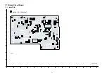
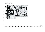
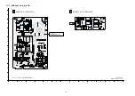
18 Appendix Information of Schematic Diagram
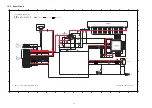
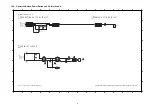
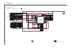
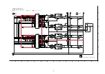
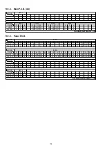
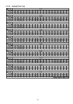
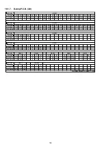
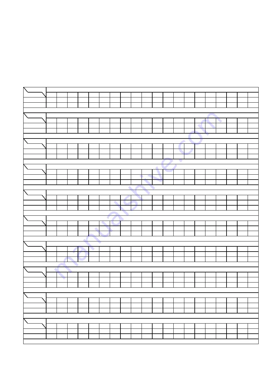
18.1. Voltage & Waveform Chart
Note:
• Indication Voltage Values are in standard values for the unit measured by the DC electronic circuit tester (high-impedance) with
the chassis taken as standard.
Therefore, there may exist some errors in voltage values, depending on the internal impedance of the DC circuit tester.
• Circuit voltage and waveform described herein shall be regarded as reference information when probing defect point because it
may differ from actual measuring value due to difference of Measuring instrument and its measuring condition and product itself.
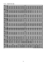
18.1.1.
Main P.C.B. (1/4)
REF NO.
MODE
1
2
3
4
5
POWER ON
3.0
0
0
5.1
3.2
STANDBY
3.0
0
0
5.1
3.3
REF NO.
MODE
1
2
3
4
5
6
7
8
9
10
11
12
13
14
15
16
17
18
19
20
POWER ON
0
1.2
3.3
0
0
0
3.3
0
0
3.3
1.6
3.3
1.5
3.3
3.3
0
0
0.9
0
3.3
STANDBY
0
1.2
3.3
0
0
0
3.3
0
0
3.3
1.6
3.3
1.5
3.3
3.3
0
0
0.9
0
3.3
REF NO.
MODE
21
22
23
24
25
26
27
28
29
30
31
32
33
34
35
36
37
38
39
40
POWER ON
3.3
3.3
3.3
1.3
2.5
1.8
3.0
3.1
0
0
0
3.2
3.3
3.3
0
3.3
3.3
0
0
0
STANDBY
3.3
3.3
3.3
1.3
2.5
1.8
3.0
3.1
0
0
0
3.2
3.3
3.3
0
3.3
3.3
3.3
0
0
REF NO.
MODE
41
42
43
44
45
46
47
48
49
50
51
52
53
54
55
56
57
58
59
60
POWER ON
0.8
0.8
3.3
0
3.3
0
0
3.3
3.3
3.3
3.3
3.3
0
0
3.3
3.3
0
0
0
3.3
STANDBY
0.8
0.8
3.3
0
3.3
0
0
3.3
3.3
3.3
3.3
3.3
0
0
3.3
3.3
0
0
0
3.3
REF NO.
MODE
61
62
63
64
65
66
67
68
69
70
71
72
73
74
75
76
77
78
79
80
POWER ON
3.3
0
0
0
0
3.2
0
0
0
0
0
0
3.3
0
3.3
3.3
0
0
3.3
0
STANDBY
3.3
0
0
0
0
3.2
0
0
0
0
0
0
3.3
0
3.3
3.3
0
0
3.3
0
REF NO.
MODE
81
82
83
84
85
86
87
88
89
90
91
92
93
94
95
96
97
98
99
100
POWER ON
3.3
0
0
0
0
3.3
0
2.0
2.1
3.2
0
0
3.2
0
3.3
3.3
3.3
0
3.0
0
STANDBY
3.3
0
0
0
0
3.3
0
2.0
2.1
3.2
0
0
3.2
0
3.3
3.3
3.3
0
3.0
0
REF NO.
MODE
1
2
3
4
5
6
7
8
POWER ON
0
0
0
0
3.3
3.3
0
3.3
STANDBY
0
0
0
0
3.3
3.3
0
3.3
REF NO.
MODE
1
2
3
4
5
6
7
8
USB
0
5.0
5.0
3.2
3.2
5.0
5.0
5.0
STANDBY
0
5.0
5.0
3.2
3.2
5.0
5.0
5.0
REF NO.
MODE
1
2
3
4
5
6
7
8
9
10
11
12
13
14
15
16
17
18
19
20
USB
1.6
2.3
2.0
1.0
1.5
0
16.0
15.6
10.6
12.0
12.7
16.2
16.3
16.3
14.3
1.7
1.0
1.9
2.4
2.4
STANDBY
1.6
2.3
2.0
1.0
1.5
0
16.0
15.6
10.6
12.0
12.5
15.7
15.7
15.9
14.0
1.7
1.0
1.9
2.4
2.4
REF NO.
MODE
1
2
3
4
5
POWER ON
9.0
0
1.3
5.1
9.4
STANDBY
9.1
0
1.3
5.0
9.4
IC2300
IC3952
SA-XH201GW MAIN P.C.B.
IC2091
IC2901
IC2300
IC2301
IC2602
IC2300
IC2300
IC2300
Summary of Contents for SA-XH201
Page 15: ...15 4 1 Others Licences ...
Page 16: ...16 5 General Introduction 5 1 Power Saving Features ...
Page 17: ...17 5 2 Linked Operations with the TV VIERA Link HDAVI Control ...
Page 18: ...18 5 2 1 Easy Control With Viera Remote Control ...
Page 19: ...19 5 3 Disc Information 5 3 1 Media that can be played ...
Page 20: ...20 5 3 2 File Extension Type Support MP3 JPEG Xvid ...
Page 21: ...21 6 Location of Controls and Components 6 1 Remote Control Key Button Operations ...
Page 22: ...22 6 2 Main Unit Key Button Operations ...
Page 24: ...24 7 3 Connection with an ARC compatible TV ...
Page 47: ...47 12 3 Main Components and P C B Locations ...
Page 76: ...76 ...
Page 78: ...78 ...
Page 122: ...122 MMH1303 ...


