38
10 Troubleshooting Guide
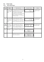
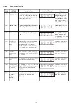
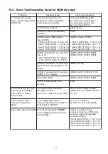
10.1. Troubleshooting Guide for F61 and/or F76
This section illustrates the checking procedures when upon detecting the error of “F61” and/or “F76” after power up of the unit. It is
for purpose of troubleshooting and checking in SMPS P.C.B..
Symptom(s)
Checking items
Possible Fault(s)
Remarks
Set cannot Power ON:
Condition 1:
With Stanby LED on
1 Photocoupler PC5702,
PC5799
1 PC5702/PC5799 solder crack,
dry joint , short circuit, open
circuit, etc
2 Switching IC IC5701
1 AC cord
2 AC Inlet P5701
1 Faulty AC cord, loose
connection
Solder crack, dry joint, short
circuit, open circuit, etc
2
Solder crack, dry joint, short
circuit,open circuit,etc
4
Check FFC connection/
alignment from SMPS (JW2)
to Main (CN2004)
2
2 P5701 solder crack, dry joint
etc
2 Faulty IC5701, pin 1 and 2
shorted, VCC short to GND, etc
3 Faulty IC5799, pin 5 and 7
shorted, VCC short to GND, etc
3 Switching IC IC5799
Set can Power ON
then F61
Set can Power ON
then F76
Set can Power ON
working normally for
sometime then F61
Condition 2:
With Stanby LED Off
or flickering
3 F1 Fuse open
3 Fuse F1
1 DC-DC circuit
1 Thermal Diode D5802
2 SMPS FFC loose
3 LDO regulator
4 Photocoupler PC5720
1 Transformer T5701
2 Photocoupler PC5720
1a Pin 11/12 shorted to pin 13/14
1b Pin 16 shorted to pin 17
1a L2902 Open (no input to
IC2901)
1b Faulty IC2901 (no output
voltage at pin 10 and 11)
1a Improper contact between
D5802 to heatsink
1b OTP (thermal) protection
trigger prematurely
3a Faulty Q2904 Transistor diode
check (cannot switch ON then
NO +9V)
3b LB2761 Open (+9V line going
to Panel PCB CN2002)
1c Faulty Q2902 and Q2903
(regulator)
1d L2908 open (No DC +5V)
1e R2399 open (No DC +9V)
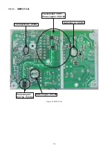
1) Refer to Figure 10-1 SMPS
P.C.B.
Refer to Figure 10-1 SMPS P.C.B.
Refer to Figure 10-1 SMPS P.C.B.
Refer to Figure 10-1 SMPS P.C.B.
Refer to Schematic Diagram of
SMPS Circuit (Item 17.6) for
terminal pin count on primary and
secondary terminals
SMPS Circuit (Item 17.6)
2) Refer to Schematic Diagram of
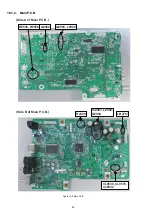
1) Refer to Figure 10-2 Main P.C.B.
Main Circuit (Item 17.2)
2) Refer to Schematic diagram of
1) Refer to Figure 10-2 Main P.C.B.
Main Circuit (Item 17.2)
2) Refer to Schematic diagram of
Summary of Contents for SA-XH201
Page 15: ...15 4 1 Others Licences ...
Page 16: ...16 5 General Introduction 5 1 Power Saving Features ...
Page 17: ...17 5 2 Linked Operations with the TV VIERA Link HDAVI Control ...
Page 18: ...18 5 2 1 Easy Control With Viera Remote Control ...
Page 19: ...19 5 3 Disc Information 5 3 1 Media that can be played ...
Page 20: ...20 5 3 2 File Extension Type Support MP3 JPEG Xvid ...
Page 21: ...21 6 Location of Controls and Components 6 1 Remote Control Key Button Operations ...
Page 22: ...22 6 2 Main Unit Key Button Operations ...
Page 24: ...24 7 3 Connection with an ARC compatible TV ...
Page 47: ...47 12 3 Main Components and P C B Locations ...
Page 76: ...76 ...
Page 78: ...78 ...
Page 122: ...122 MMH1303 ...


