background image

© Panasonic Corporation 2011. All rights reserved.
Unauthorized copying and distribution is a violation
of law.

PSG1104002CE

A6

DVD Home Theater Sound System

Model No.

SA-XH50P
SA-XH50PC

Product Color: (K)...Black Type

TABLE OF CONTENTS

PAGE

PAGE

1 Safety Precautions----------------------------------------------- 3

1.1. GENERAL GUIDELINES -------------------------------- 3
1.2. Before Repair and Adjustment ------------------------- 4
1.3. Protection Circuitry ---------------------------------------- 5
1.4. Safety Parts Information --------------------------------- 5

2 Warning -------------------------------------------------------------- 6

2.1. Prevention of Electrostatic Discharge (ESD)

to Electrostatic Sensitive (ES) Devices--------------- 6

2.2. Precaution of Laser Diode ------------------------------- 7
2.3. Service caution based on Legal restrictions -------- 8
2.4. Handling Precautions for Traverse Unit -------------- 9

3 Service Navigation --------------------------------------------- 11

Note: Please refer to the original service manual for:

O


DVD Mechanism Unit (BRS1D), Order No. PSG1012001CE

O

 Speaker system SB-XH50P/PC-K, Order No. PSG1103007CE

Summary of Contents for SA-XH50P

Page 1: ...efore Repair and Adjustment 4 1 3 Protection Circuitry 5 1 4 Safety Parts Information 5 2 Warning 6 2 1 Prevention of Electrostatic Discharge ESD to Electrostatic Sensitive ES Devices 6 2 2 Precaution of Laser Diode 7 2 3 Service caution based on Legal restrictions 8 2 4 Handling Precautions for Traverse Unit 9 3 Service Navigation 11 Note Please refer to the original service manual for O DVD Mech...

Page 2: ...anism Unit BRS1D 52 10 9 Replacement of Traverse unit 54 10 10 Disassembly of Main P C B 59 10 11 Replacement of Digital Amplifier IC IC403 IC404 IC405 61 10 12 Disassembly of SMPS P C B 63 10 13 Replacement of Current Limiting Switch Q5701 65 10 14 Replacement of Diode D5706 66 10 15 Disassembly of Backend P C B 67 11 Service Position 69 11 1 Checking Repairing Main P C B Side B 69 11 2 Checking ...

Page 3: ... for safety 3 Check the condition of the power cord Replace if wear or damage is evident 4 After servicing be sure to restore the lead dress insulation barriers insulation papers shields etc 5 Before returning the serviced equipment to the customer be sure to make the following insulation resistance test to prevent the customer from being exposed to a shock hazard 1 1 2 LEAKAGE CURRENT HOT CHECK 1...

Page 4: ...esis tor to ground Caution DO NOT SHORT CIRCUIT DIRECTLY with a screwdriver blade for instance as this may destroy solid state devices After repairs are completed restore power gradually using a variac to avoid overcurrent Current consumption at AC 120V 60 Hz in NO SIGNAL mode at volume minimal should be 200 mA 1 2 1 Caution for fuse replacement ...

Page 5: ...marked by in the Schematic Diagrams Exploded View Replacement Parts List It is essential that these critical parts should be replaced with manufacturer s specified parts to prevent shock fire or other hazards Do not modify the original design without permission of manufacturer Safety Ref No Part No Part Name Description Remarks 8 RGRX1004B A REAR PANEL P 8 RGRX1004B B1 REAR PANEL PC 20 RKMX1009 K ...

Page 6: ...of the assembly 3 Use only a grounded tip soldering iron to solder or unsolder ES devices 4 Use only an anti static solder removal device Some solder removal devices not classified as anti static ESD protected can generate electrical charge sufficient to damage ES devices 5 Do not use freon propelled chemicals These can generate electrical charges sufficient to damage ES devices 6 Do not remove a ...

Page 7: ...t radiation power from pickup 100 µW VDE Laser radiation from the pickup unit is safety level but be sure the followings 1 Do not disassemble the pickup unit since radiation from exposed laser diode is dangerous 2 Do not adjust the variable resistor on the pickup unit It was already adjusted 3 Do not look at the focus lens using optical instruments 4 Recommend not to look at pickup lens for a long...

Page 8: ...is used Definition The letter of PbF is printed on the PCB using the lead free solder To put lead free solder it should be well molten and mixed with the original lead free solder Remove the remaining lead free solder on the PCB cleanly for soldering of the new IC Since the melting point of the lead free solder is higher than that of the normal lead solder it takes the longer time to melt the lead...

Page 9: ...the laser diode from the electrostatic discharge damage the flexible cable of the optical pickup unit removed should be short circuited with a short pin or a clip 3 The flexible cable may be cut off if an excessive force is applied to it Use caution when handling the flexible cable 4 The antistatic FPC is connected to the new optical pickup unit After replacing the optical pickup unit and connecti...

Page 10: ...10 2 4 2 2 Human body grounding 1 Use the anti static wrist strap to discharge the static electricity form your body Figure 2 ...

Page 11: ...rders using the parts list and not the drawing reference numbers If the circuit is changed or modified this information will be followed by supplement service manual to be filed with original service manual DVD Mechanism Unit BRS1D 1 This model uses DVD Mechanism Unit BRS1D Micro processor 1 The following components are supplied as an assembled part Micro processor IC IC200 RFKWMXH50EB ...

Page 12: ... Terminal Sampling frequency 32 kHz 44 1 kHz 48 kHz Music Port Front Sensitivity 100 mV 6 8 kΩ Terminal Stereo 3 5 mm 1 8 jack ODISC SECTION Discs played 8 cm or 12 cm 1 DVD DVD Video 2 DVD RW DVD Video MP3 2 4 JPEG 3 4 3 DVD R DL DVD Video 4 DVD RW DVD Video MP3 2 4 JPEG 3 4 5 R RW Video 6 R DL Video 7 CD CD R RW CD DA Video CD SVCD 1 MP3 2 4 JPEG 3 4 1 Conforming to IEC62107 2 MPEG 1 Layer 3 MPE...

Page 13: ...13 4 1 Others Licences ...

Page 14: ...14 5 Location of Controls and Components 5 1 Remote Control and Main Unit Key Button Operations ...

Page 15: ...r consumption and save energy Auto power down function The main unit will automatically switch to standby mode after 30 minutes of inactivity e g There is no audio signal from an external device Disc playback is stopped paused The disc menu is displayed and play is not selected This function may not work depending on the application type of discs g ...

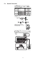
Page 16: ...16 5 4 Speaker Connection ...

Page 17: ...17 5 5 Linked Operations with the TV VIERA LINK HDAVI Control ...

Page 18: ...18 ...

Page 19: ...19 5 6 Connection with an ARC compatible TV ...

Page 20: ...mats Indicated as DVD R RW DVD Video Format MP3 format JPEG format MP3 MP3 JPEG JPEG DVD R DL DVD Video Format R RW R DL VR R RW Video Recording Format CD R RW CD DA format MP3 format JPEG format Note about using a DualDisc The digital audio content side of a DualDisc does not meet the technical specifications of the Compact Disc Digital Audio CD DA format so playback may not be possible Discs tha...

Page 21: ...21 5 7 2 File Extension Type Support MP3 JPEG ...

Page 22: ... 6 1 1 2 When the power cannot be turned off 1 Press hold the POWER button to turn off the power forcibly then press hold SKIP FWD button on remote and OPEN CLOSE button on main unit for 5 seconds 6 1 2 When the Forcible Disc Eject cannot be done 1 Turn off the power and remove AC cord 2 Insert Paper Clip into the hole on the bottom of unit and slide the Paper Clip on the direction of the arrow to...

Page 23: ...23 3 Gently pull out the tray 4 Remove disc ...

Page 24: ..._ _ _ _ 4 Release POWER button 7 2 Service Mode Table By pressing various button combinations on the main unit and remote control unit you can activate the various service modes for checking Special Note Due to the limitations of the no characters that can be shown on the FL Display the FL Display button on the remote control unit can be used to show the two display pages Display 1 Display 2 Refer...

Page 25: ... the main unit and 5 button on the remote control unit Press FL Display on remote control unit for next page FL Display Error code check Error code check The latest error code stored in the EEPROM IC is displayed Note Refer to Section 7 4 Self Diagnostic Function Error Code for more detailed information on the error codes Error code play_err is expressed in the following convention Error code 0 x ...

Page 26: ...ress Power Off Button on remote control The value denotes the current in decimal notation DVD laser current measurement mode DVD laser drive current measurement For DVD laser drive current refer to Troubleshooting Guide Section 8 2 CD laser drive current measurement For CD laser drive current refer to Troubleshooting Guide Section 8 2 Region code display TV broadcasting system the model no informa...

Page 27: ...tate of EEPROM IC FL Display sequence Display 1 2 3 In STOP no disc mode press OPEN CLOSE button on the main unit and 10 button on the remote control unit Cancelled automatically 5 seconds later In STOP no disc mode press OPEN CLOSE button on the main unit and 7 button on the remote control unit Press FL Display button on remote control unit for next page FL Display Display 2 If the version of the...

Page 28: ...ly 5 seconds later In STOP no disc mode press OPEN CLOSE button on the main unit and button on the remote control unit Timer 1 reset Timer 2 check Timer 2 reset Timer 1 check Laser operation timer is measured separately for DVD laser and CD laser FL Display sequence Display 1 2 Timer 1 reset Laser operation timer of both DVD laser and CD laser is reset all at once Timer 2 check Spindle motor opera...

Page 29: ...W Europe Middle East Africa S E A Country OSD Language OSD Default English English English English English NA Traditional Chinese GW 5 PAL PAL C 5PP India English English English English English GK English NA Simplified Chinese 6 PAL 6PN China Simplified Chinese Japanese English NA Spanish Panama French Brazilian Portuguese PN 4 NTSC Central S America Brazil Spanish NTSC D 4PN English NA Spanish P...

Page 30: ...ress hold OPEN CLOSE on main unit follow by 4 then 9 on remote control When no disc in mechanism System will clear all of the contents of unusual error code from the memory FL Display Key Operation Front Key Item Description Mode Name In self diagnostic mode press STOP on remote control To exist press on main unit or remote control In self diagnostic mode press CANCEL on remote control To exist pr...

Page 31: ...Press OPEN CLOSE on on communication error connecting it with HDMI DVI For main unit for next error Press OPEN CLOSE on main unit for next error Press OPEN CLOSE main unit for next error on Press OPEN CLOSE main unit for next error on Press OPEN CLOSE main unit for next error instance when EDID information to which information on the TV set side has been described cannot be read it is generated U7...

Page 32: ...s due to speaker output has DC voltage F76 Abnormality in the In normal operation when DCDET1 is output voltage of detected L Low for two consecutive stabilized power times F76 is displayed on FL for supply 1 second and after that PCONT will be turned to L Low This is due to any of the DC voltages 9V 7V 7V 5V 5 3V etc not available Diagnosis Contents Description of error Automatic FL Display Remar...

Page 33: ...unction mode is entered Prohibiting operation of selector and disc 1 Select the DVD CD function 2 At POWER ON condition press and hold down the OPEN CLOSE button and the VOL button on the main unit for at least three seconds The message LOCKED appears when the function is activated Note The following buttons are invalid and the main unit displays LOCKED while the lock function mode is entered 7 5 ...

Page 34: ...can put both files into the same root directory DVD MODEL will choose the right ROM files to update its firmware FL GUI Display Remarks Item Description Process 1 2 Display 1 GUI Display 1 1 Step 1 Power on main unit Step 2 Change selector to CD DVD mode default is DVD CD mode Step 3 Load in the disc with software firmware update data After disc reading GUI will display as GUI Display 1 1 Are you ...

Page 35: ...cessfully GUI Display 1 3 Firmware update is completed please open the tray and remove the disc GUI Display 1 3 Step 5 Eject the disc and power off main unit Step 6 Power on the unit and do system initialize Step 7 Update process finish FL GUI Display Remarks Item Description Process FL Display 1 6 FL Display Main Unit will display GOOD as FL Display 1 6 shown ...

Page 36: ... 3 1 2 3 3 F1 Fuse open Fuse F1 DC DC circuit 1 Thermal Diode D5706 SMPS FFC loose Voltage regulator 4 Photocoupler PC701 1 Transformer T5701 2 Photocoupler PC701 1a Pin 14 15 shorted to pin 12 13 1a 1b L421 Open no input to IC106 Faulty IC106 no output voltage at pin 3 1a 1b Improper contact between D5706 to heatsink OTP thermal protection trigger prematurely 3a Faulty Q107 Transistor diode check...

Page 37: ...37 8 1 1 SMPS P C B Fig 1 SMPS P C B AC Inlet Jack P5701 Fuse F1 Regulator IC IC2900 Thermal Diaod D5706 Photocoupler PC701 H2016 FFC Conector H2016 Transformer T5701 ...

Page 38: ...38 8 1 2 Main P C B Fig 2 Main P C B Conector CN100 Transistor Q107 Resistor R100 Inductors L421 Chip Jumper K304 DC DC CONVERTER IC IC106 Inductors L125 ...

Page 39: ...ltage across R8566 which has a resistance value of 4 7 ohm 2 Calculate the CD Laser current by the following formula CD_LD VCD 4 7 1 Measurement the voltage VDVD on the testpoints CL8530 CL8532 This is voltage across R8556 which has a resistance value of 4 7 ohm 2 Calculate the DVD Laser current by the following formula DVD_LD VCD 4 7 Refer to 8 2 1 Backend P C B Fig 3 Backend P C B Refer to 8 2 1...

Page 40: ...40 8 2 1 Backend P C B Fig 3 Backend P C B CL8530 CL8531 CL8532 R8556 R8566 Side A of Backend P C B Side B of Backend P C B ...

Page 41: ...94 95 IC8251 Pin 11 to 18 Check for solder short and or component missing damaged a Check connection from Main to Traverse unit FP8251 3 Disc not spinning 4 Traverse not moving 5 Traverse and spindle abnormal movement b Check motor driver circuitry on the voltages and control signals Compare the above with OK condition Main P C B IC8251 Check for solder short and or component damaged 6 Cannot read...

Page 42: ...tter communication lines to TV 6 HDMI Transmitter communication from LSI IC8001 3 3V Supply 7 HDMI Transmitter LSI IC IC8001 1 8 V Supply 8 Hot Plug Signal 9 HDMI Interface Reference Resistor 1 Supply fo HDMI transmitter intergrated IC8001 2 Check for Capacitor short to GND Check Digital Signal Data communication lines from IC8001 to Serial Flash IC IC8651 Check the setting under SETUP menu if HDM...

Page 43: ... 9 Service Fixture Tools 9 1 Service Tools and Equipment Prepare service tools before process service position Ref No Service Tools Remarks SFT1 Main P C B CN201 Backend P C B FP8101 RFKZXH150PK2 50P FFC ...

Page 44: ...er prolong use See caution as described below During disassembly and assembly please ensure proper service tools equipments or jigs is being used During replacement of component parts please refer to the section of Replacement Parts List as described in the service manual Select items from the following indexes when disassembly or replacement are required Disassembly of Top Cabinet Disassembly of ...

Page 45: ...m Unit BRS1D 10 15 Backend P C B 10 5 Front Panel Assembly 10 6 Panel P C B 10 4 Rear Panel 10 7 Power Button P C B 10 12 SMPS P C B 10 13 Current Limiting Switch Q5701 10 14 Diode D5706 10 10 Main P C B 10 11 Digital Amplifier IC IC403 IC404 IC405 10 9 Traverse Unit ...

Page 46: ...46 10 2 Main Components and P C B Locations ...

Page 47: ...p back of Top Cabinet as arrow shown Step 5 Press location A in downward direction at Front Panel Step 6 Remove Top Cabinet as arrow shown Caution Replace the Top Cabinet Insulator sheet if broken Ensure it is pasted properly on Top Cabinet as diagram shown Caution During assembling ensure taht the catches of Top Cabinet is inserted into Front Panel properly ...

Page 48: ... of arrow Step 4 Remove Rear Panel 10 5 Disassembly of Front Panel Assembly Refer to Disassembly of Top Cabinet Step 1 Detach 17P FFC at the connector CN203 on Main D Amp P C B Step 2 Lift up 2 Himelons Caution Replace the Himelons if it is torn Step 3 Release the 2 tabs at each side of the Front Panel Assembly in the direction of arrow Step 4 Release the 3 tabs at the bottom chassis ...

Page 49: ...nt Panel Assembly Step 1 Remove 5 screws Step 2 Remove 1 screw Step 3 Lift up Panel P C B Caution During assembling ensure that Panel P C B is properly located and fully fixed onto Front Panel Step 4 Release 3P wire from wall ribs of Front Panel Caution During assembling ensure that 3P wie is prop erly dressed in between wall ribs of Frant Panel as dia gram shown Step 5 Remove Ground Spring ...

Page 50: ...round Spring in safe place place it back during assembling Step 6 Desolder 3P Wire at the cable holder H902 on Panel P C B Step 7 Remove Panel P C B Caution During assembling ensure that 17P FFC is dressed as diagram shown ...

Page 51: ...C B as direction of arrow Caution During assembling ensure that Power Button P C B is fully catched Step 3 Release 3P wire from wall ribs of Front Panel Caution During assembling ensure that 3P wire is prop erly dressed in between wall ribs of Front Panel as dia gram shown Step 4 Desolder 3P wire at the cable holder H901 on Power Button P C B Step 5 Remove Power Button P C B ...

Page 52: ...ttom Chassis Assembly Step 2 Push the Paper Clip in the direction of the arrow to eject Tray Step 3 Slide the Tray out fully as direction of arrow Step 4 Upset the Unit Step 5 Release 2 catches Caution During assembling ensure that Tray Ornament is inserted fully catched onto Tray Step 6 Remove Tray Ornament in the direction of arrow ...

Page 53: ... the Tray in fully Step 8 Detach 24P FFC at the connector FP8531 on Backend P C B Step 9 Detach 6P FFC at the connector FP8251 on Backend P C B Step 10 Detach 5P FFC at the connector FP8252 on Backend P C B Caution During assembling dress the 5P FFC under Rib A and behind Rib B properly Step 11 Remove 4 screws ...

Page 54: ...m Chasiss before screwing 10 9 Replacement of Traverse unit Refer to Disassembly of DVD Mechanism Unit BRS1D Caution Refer to 2 4 Handling Precaution for Traverse Unit to prevent static damage to the Optical Pickup unit Note 1 When the optical pickup unit is defective the overall traverse unit needs replacement 2 Please note that appropriate actions need to be taken to prevent static damage 10 9 1...

Page 55: ...55 Step 2 Slide the tray out fully Step 3 Release the catches remove the tray Step 4 Release the guide as shown slide the Traverse Slide Plate to the end Step 5 Release the 24P FFC from the slot ...

Page 56: ...by approximately 45 Step 7 Slide out the traverse unit as arrow shown Caution Avoid touching the surface of the traverse unit 10 9 2 Assembly of Traverse Unit Step 1 Release the guide as shown slide the Traverse Slide Plate to the end ...

Page 57: ...lot the Traverse unit at approximately 45 into the mecha chassis as arrow shown Step 3 Ensure the Traverse Unit seated properly onto the Groove Step 4 Slide Traverse Slide Plate to lock the Traverse Unit as shown ...

Page 58: ...that the FFC are properly inserted into the slots as shown Step 6 Slide the Traverse Slide Plate unit it stop at the Guide Step 7 Slot the Tray into the Guides as picture shown Step 8 Ensure the Guides are align with the groove when slid ing the tray in ...

Page 59: ... Top Cabinet Step 1 Remove 5 screws Step 2 Remove 1 screw Step 3 Position Rear Panel according to diagram shown Step 4 Detach 50P FFC at the connector CN201 on Main P C B Step 5 Detach 17P FFC at the connector CN203 on Main P C B Step 6 Detach 12P cable at the connector CN100 on Main P C B ...

Page 60: ...60 Step 7 Remove 2 screws on Main P C B Step 8 Remove Main P C B Caution During assembling ensure that Main P C B is properly located fully seated onto Bottom Chassis ...

Page 61: ...acement of Digital Ampli fier IC IC403 IC404 IC405 Refer to Disassembly of Top Cabinet Refer to Disassembly of Main P C B 10 11 1 Disassembly of Digital Amplifier IC IC403 IC404 IC405 Caution Handle the Main P C B with caution due to it s high temperature after prolonged use Step 1 Place Main P C B on an insulated material Step 2 Remove 3 screws ...

Page 62: ...er IC IC404 IC405 repeat the Step 1 to Step 5 of 10 11 1 Note 2 Refer to diagram of Main P C B item 18 2 for location of part 10 11 2 Assembly of Digital Amplifier IC IC403 IC404 IC405 Step 1 Fix the Digital Amplifier IC IC403 onto the Main P C B Step 2 Solder pins of Digital Amplifier IC IC403 Caution Ensure that the pins of Digital Amplifier IC IC5100 is positioned correctly on Main P C B before...

Page 63: ...sembling of Digital Amplifier IC IC404 IC405 repeat the Step 1 to Step 5 of 10 11 2 10 12 Disassembly of SMPS P C B Refer to Disassembly of Top Cabinet Step 1 Remove 5 screws Step 2 Release tab at left side of the Rear Panel in the direction of arrow Step 3 Detach 12P cable at the connector CN100 on Main P C B ...

Page 64: ...he SMPS P C B with care Avoid touching the heatsink due to its prolong use Caution During assembling ensure that SMPS P C B is properly located fully inserted onto Bottom Chassis Caution Replace the Bottom PC Sheet if broken Ensure that it is pasted on the Bottom Chassis properly ...

Page 65: ...igh temperature after prolonged use Touching it may lead to injuries Note Refer to the diagrams of SMPS P C B Item 18 4 for location of the part 10 13 2 Assembly of Current Limiting Switch Q5701 Step 1 Apply grease to the Heatsink Ext A Step 2 Fix the Current Limiting Switch Q5701 to the SMPS P C B Caution Ensure pins of the Current Limiting Switch Q5701 are properly seated and soldered on SMPS P ...

Page 66: ... its high temperature after prolonged use Touching it may lead to injuries Note Refer to the diagrams of SMPS P C B Item 18 4 for location of the part 10 14 2 Assembly of Diode D5706 Step 1 Apply grease to the Heatsink Ext B Step 2 Fix the Diode D5706 to the SMPS P C B Caution Ensure pins of the Diode D5706 are properly seated and soldered on SMPS P C B Step 3 Fix and screw the Diode D5706 to the ...

Page 67: ... at the connector FP8531 on Backend P C B Step 5 Detach 6P FFC at the connector FP8251 on Backend P C B Step 6 Detach 5P FFC at the connector FP8252 on Backend P C B Step 7 Detach 5P Cable at the connector FP9001 on Back end P C B Step 8 Detach 50P FFC at the connector FP8101 on Backend P C B Step 9 Remove 2 screws Step 10 Lift up the Backend P C B Step 11 Release the Locator to remove Backend P C...

Page 68: ...rly inserted and fully seated onto Backend P C B Caution During assembling replace the B E Heat Radia tor if torn Ensure that B E Heat Radiator is properly located fully pasted within embossing on Backend P C B Shield Plate Caution During assembling ensure that Backend P C B is properly located fully seated onto Bottom Chassis ...

Page 69: ... CN100 on Main P C B Step 7 Connect 50P FFC the connector CN201 on Main P C B Step 8 Connect 17P FFC the connector CN203 on Main P C B Step 9 Proceed to check repair Main P C B Side B 11 2 Checking Repairing Main P C B Side A Step 1 Remove Top Cabinet Step 2 Remove Rear Panel Step 3 Remove 2 screws Step 4 Detach 50P FFC the connector CN201 on Main P C B Step 5 Position Main P C B on the insulated ...

Page 70: ...B Step 1 Remove Top Cabinet Step 2 Remove Panel P C B Power Button P C B Step 3 Position Panel P C B Power Button P C B on the insu lated material as diagram shown Step 4 Connect 17P FFC at the connector CN203 on Main P C B Step 5 Proceed to check and repair Panel P C B 11 5 Checking Repairing of DVD Module P C B 11 5 1 Checking Repairing of Backend P C B Side B Step 1 Remove Top Cabinet Step 2 Re...

Page 71: ...tor FP8531 on Back end P C B Step 4 Connect 6P FFC at the connector FP8251 on Backend P C B Step 5 Connect 5P FFC at the connector FP8252 on Backend P C B Step 6 Connect 50P FFC at the connector FP8101 on Back end P C B Step 7 Flip the Backend P C B and position it onto Insulated material Step 8 Proceed to check repair side A of Backend P C B ...

Page 72: ...33 34 35 36 37 38 39 40 CD PLAY 1 1 1 0 0 5 1 1 1 1 0 6 3 0 0 7 1 1 0 1 1 1 0 6 0 6 1 7 3 0 0 1 5 1 5 0 0 STANDBY 1 5 3 1 2 8 1 6 0 3 2 8 3 3 0 6 0 4 0 5 0 5 0 2 6 1 8 3 2 0 1 5 1 5 0 0 REF NO MODE 41 42 43 44 45 46 47 48 49 50 51 52 53 54 55 56 57 58 59 60 CD PLAY 0 0 1 4 1 5 3 0 3 0 3 0 2 9 0 0 0 0 0 0 0 0 3 0 0 9 1 7 1 7 STANDBY 0 0 1 5 1 5 3 1 3 0 3 1 3 0 0 0 0 0 0 0 0 0 3 1 0 9 1 7 1 7 REF NO...

Page 73: ... 7 0 REF NO MODE 1 2 3 4 5 CD PLAY 3 4 3 4 0 1 9 0 8 STANDBY 3 5 3 5 0 1 9 0 8 REF NO MODE 1 2 3 4 5 6 7 8 CD PLAY 3 1 0 0 1 8 4 7 0 0 4 7 STANDBY 3 1 0 0 1 8 4 7 0 0 4 8 REF NO MODE 1 2 3 4 5 6 7 8 9 10 11 12 13 14 15 16 17 18 19 20 CD PLAY 1 6 8 9 2 1 1 6 2 0 3 1 3 1 8 9 0 0 4 5 4 5 2 4 2 5 2 5 2 5 3 4 1 6 4 8 1 9 STANDBY 1 3 8 9 2 3 1 3 2 3 3 2 3 2 9 2 0 0 2 0 0 1 4 1 4 1 4 1 4 1 3 1 3 4 9 2 3 ...

Page 74: ...AY 0 3 0 1 1 3 0 4 7 3 1 3 0 4 8 3 1 3 1 3 1 2 8 3 1 2 3 2 4 STANDBY 0 3 0 1 1 3 1 4 7 3 1 3 1 4 7 3 1 3 1 3 0 2 8 3 3 0 3 3 REF NO MODE E C B E C B CD PLAY 3 3 0 1 3 3 0 1 0 1 0 7 STANDBY 3 3 0 3 3 0 4 8 0 Q8562 Q8565 SA XH50P PC BACKEND P C B Q3901 Q3902 Q3903 Q3904 Q8552 ...

Page 75: ... 3 3 2 0 0 0 0 3 2 0 0 3 3 3 3 0 0 3 3 3 3 0 0 0 3 3 STANDBY 1 3 1 3 3 2 0 0 0 0 3 2 0 0 3 3 3 3 0 0 3 3 3 3 0 0 0 3 3 REF NO MODE 61 62 63 64 65 66 67 68 69 70 71 72 73 74 75 76 77 78 79 80 CD PLAY 0 0 1 3 3 2 0 3 3 0 1 3 1 3 0 3 2 0 3 2 0 3 3 3 2 0 0 3 2 3 2 STANDBY 0 0 1 3 3 2 0 3 3 0 1 3 1 3 0 3 2 0 3 2 0 3 3 3 2 0 0 3 2 3 2 REF NO MODE 81 82 83 84 85 86 87 88 89 90 91 92 93 94 95 96 97 98 99 ...

Page 76: ...MODE 1 2 3 4 5 6 7 8 9 10 11 12 13 14 15 16 17 18 19 20 CD PLAY 3 3 3 3 0 0 3 3 0 3 3 0 0 0 0 0 0 0 0 0 3 3 0 0 0 STANDBY 3 3 3 3 0 0 3 3 0 3 3 0 0 0 0 0 0 0 0 0 3 3 0 0 0 REF NO MODE 21 22 23 24 25 26 27 28 29 30 31 32 33 34 35 36 37 38 39 40 CD PLAY 3 3 3 3 3 3 10 1 0 20 3 20 3 10 1 0 0 10 2 20 3 10 2 10 2 20 3 10 2 0 0 10 2 20 3 STANDBY 3 3 3 3 3 3 10 1 0 20 3 20 3 10 1 0 0 10 2 20 3 10 2 10 2 ...

Page 77: ... 3 0 2 8 3 3 3 3 0 2 8 2 8 2 8 0 2 8 0 0 0 STANDBY 0 2 8 0 0 0 0 3 3 0 2 8 3 3 3 3 0 2 8 2 8 2 8 0 2 8 0 0 0 REF NO MODE 1 2 3 4 5 6 7 8 9 10 11 12 13 14 15 16 CD PLAY 2 4 2 4 0 2 4 0 4 8 3 3 0 1 2 1 4 1 5 1 5 3 1 3 1 0 0 STANDBY 2 4 2 4 0 2 4 0 4 8 3 3 0 1 2 1 4 1 5 1 5 3 1 3 1 0 0 REF NO MODE 1 2 3 4 5 6 E C B E C B E C B CD PLAY 4 9 4 9 0 4 5 0 4 9 4 9 0 0 2 7 5 3 5 6 25 4 0 3 2 0 4 STANDBY 4 9...

Page 78: ...3 0 25 5 11 1 25 1 22 9 22 9 22 9 22 9 22 9 22 9 22 9 22 9 REF NO MODE 41 42 43 44 POWER ON 22 9 22 8 3 3 0 STANDBY 22 9 22 8 3 3 0 REF NO MODE E C B E C B POWER ON 0 0 2 8 3 2 2 5 2 4 STANDBY 0 0 2 8 3 2 2 5 2 4 SA XH50P PC PANEL P C B IC901 IC901 IC901 Q900 Q901 REF NO MODE 1 2 3 4 5 POWER ON 20 1 12 1 0 1 2 2 5 STANDBY 20 1 12 1 0 1 2 2 5 REF NO MODE 1 2 3 4 5 6 7 8 POWER ON 0 0 0 5 0 2 7 0 6 1...

Page 79: ...c div WF No IC401 20 PLAY 1Vp p 20nsec div WF No IC401 42 43 44 45 46 47 PLAY 6Vp p 1usec div WF No IC401 28 29 PLAY 3 2Vp p 500nsec div WF No IC401 49 50 51 52 PLAY 6Vp p 500nsec div WF No IC401 30 31 PLAY 3 6Vp p 500nsec div WF No IC401 40 41 PLAY 6Vp p 1usec div WF No IC403 6 8 16 18 PLAY 6Vp p 1usec div WF No IC404 6 8 16 18 PLAY 6Vp p 1usec div WF No IC403 28 31 36 39 PLAY 32Vp p 1usec div WF...

Page 80: ... Table 2 2 WF No IC600 2 13 14 PLAY 0 4Vp p 200usec div WF No IC8001 111 112 PLAY 2Vp p 20nsec div WF No IC8001 36 42 PLAY 4 8Vp p 2usec div WF No IC8001 63 PLAY 1 25Vp p 50usec div WF No IC8001 102 PLAY 5Vp p 1usec div ...

Page 81: ...263 B0BC5R6A0266 B0BC010A0267 B0BC015A0264 B0JCPG000005 B0JCME000035 B0BC2R4A0263 B0BC027A0264 B0EBNR000045 B0BC02700039 B0EAMM000057 B0EAKT000063 B0HBSM000054 C0DBAYH00005 RFKWMXH50EB 100P C0CBCDC00063 C0DBZYY00311 C1AB00003216 64P C1AB00003476 128P C0HBB0000057 44P B1ADCE000012 B1ABDF000026 B1ABCF000176 B1GBCFJJ0051 B1CERS000002 B1ABCF000011 B1BABK000001 B1BABD000001 B1CFHA000002 B1GBCFGG0030 B1...

Page 82: ...82 ...

Page 83: ...S BLOCK AC IN PANEL BLOCK FL DISPLAY FL Driver Power Button Open Close Button LED DVD Mechanism BRS1D MAIN BLOCK 36V PGND PCONT ECO CTL DC DET 18V DAP TUNER AUX DC DC Conveter Conveter FL Supply I2 C IR Sensor 5 3V 9V Vref ADC I 2 C DVD Decoder HDMI IC ADC Video Buffer HDMI D IN MUX Composite Motor Driver 9V UART CP IC FLASH SDRAM I 2 C MUX SEL I2 C DC DC 5 3V 5 3V I 2 S MCLK BCLK SRCK I2 S MCLK B...

Page 84: ...TK 26 TRK DRV 93 TRK DRV VINFC 1 FOC DRV 90 FOC DRV 16 VOTK 21 FP8531 T 14 VOFC 23 FP8531 F 6 FP8531 CD LD 13 VOFC 24 FP8531 F OPEN SW OPEN SW 10 41 FP8101 CN201 OPEN SW SRCK 35 16 FP8101 CN201 37 14 FP8101 CN201 SRCK LRCK LRCK MCLK 45 6 FP8101 CN201 MCLK DMIX 33 18 FP8101 CN201 SDATA3 AOUT2 39 12 FP8101 CN201 SDATA2 AOUT1 41 10 FP8101 CN201 SDATA1 AOUT0 43 8 FP8101 CN201 14 37 FP8101 CN201 SDATA0...

Page 85: ...DQ6 DQ7 DQ8 DQ9 DQ10 DQ11 DQ12 DQ13 DQ14 DQ15 53 IC8051 SDRAM IC8001 DVD DECODER TXD0P 52 TXD0 7 D0 TXD0N 51 TXD0 9 D0 TXD1P 54 TXD1 4 D1 TXD1N 53 TXD1 6 D1 TXD2P 56 TXD2 1 D2 TXD2N 55 TXD2 3 D2 IC8001 DVD DECODER P3901 HDMI AV OUT ARC SIGNAL NAME TC 3 PIN NO PORT NAME PIN NO PORT NAME SIGNAL NAME TC 1 PIN NO PORT NAME PIN NO PORT NAME 125 MA 0 23 123 MA 1 24 126 MA 2 25 121 MA 3 26 122 MA 4 29 12...

Page 86: ... DET1 55 DC DET1 DC DET1 OPEN SW OPEN SW CLOSE SW 1 CLOSE SW CLOSE SW DVD RX 27 DVD RX DVD RX VOL S906 VOL S905 DAP RST 79 DAP RST DAP MUTE 32 DAP MUTE DAP RST DAP MUTE PCONT 48 PCONT ECO CNTRL 2 ECO CNTRL PCONT ECO CNTRL FWD 36 FWD REV 37 REV FWD AMUTE 38 AMUTE AMUTE DVD TX 28 DVD TX DVD TX REV SELECTOR LSB DAP CLK TUN RST 21 TUN REST TUN REST DAP SDA CEC IN OUT 15 CEC IN OUT CEC IN OUT TUN INT T...

Page 87: ...TUN RCH AUX L AUX R AUX L AUX R SCLK 7 SDIO 8 TUN SCLK TUN SDIO I2S IN RSTB L0 1 R0 12 L2 2 R2 15 A LSB 10 B MSB 9 SELECTOR C0JBAR000540 IC300 AINL 2 AINR 1 DIGITAL AUDIO ADC C0FBAK000026 IC700 TUN LCH TUN RCH TUN SCLK TUN REST RST 5 TUN REST GCGPIO2 18 TUN INT TUN REST TUN SDIO TUN INT TUN INT VIDEO OUTPUT SIGNAL LINE RSTB MAIN P C B SELECTOR LSB SELECTOR LSB Q301 SWITCH Q300 SWITCH SELECTOR MSB ...

Page 88: ... RESET 11 MUTE 14 DAP MUTE DAP PDN PDN 13 DAP PDN DAP RST DC DET2 SD VALID SD VALID 5 SD 7 RST AB 17 RST CD 2 OTW 5 SD 7 RST AB 17 RST CD 2 OTW 5 SD 7 RST AB 17 RST CD 2 OTW 16 PWM C 18 PWM D DIGITAL AMPLIFIER C1AB00003217 IC404 6 PWM A 8 PWM B SURROUND LEFT OUT B BST B OUT A BST A 11 JK401 12 JK401 36 34 39 43 SURROUND RIGHT OUT C BST C OUT D BST D 9 JK401 10 JK401 31 33 28 24 16 PWM C 18 PWM D D...

Page 89: ...C5701 TH5701 TH5702 D5701 L5701 P5701 1 4 2 3 L5702 1 4 2 3 1 5 8 7 3 MAIN TRANSFORMER T5701 14 15 12 13 CTRL 7 VCC 1 PROT 6 DRIVER 3 ISENSE 4 D5706 D5703 D5705 3 4 2 1 PC701 FEEDBACK VINS 5 HOT COLD Q5701 CURRENT LIMITING SWITCH SHUNT REGULATOR C0DBZMC00006 IC5702 FEEDBACK CIRCUIT SWITCHING TRANSFORMER T2900 8 9 5 1 3 2 D2903 D2906 D2909 D2908 Q2900 POWER SAVE CONTROL AC INLET SMPS P C B FROM SYS...

Page 90: ...O SYSTEM CONTROL NOTE REF IS FOR INDICATION ONLY DC DETECT Q106 DC DET1 DC DETECT Q105 DC DET1 5V REGULATOR C0CBCDC00063 IC3952 3 3V REGULATOR C0DBZYY00018 IC8112 1 8V REGULATOR C0DBEHG00006 IC8111 BACKEND P C B HIGH SIDE SWITCH C0DBZYY00311 IC9006 SWITCH Q201 SWITCH Q200 DC DET2 3 G 4 S D 1 D 2 D 5 D 6 POWER SUPPLY Q100 D8101 D8102 23 24 27 28 FP8101 CN201 PW 9V M 9V 49 2 FP8101 CN201 PW 3 3VREF ...

Page 91: ...1 5 2 4 1 2 24 23 1 5 2 6 50 1 1 2 JK300 JK401 JK600 FM ANT CN201 CN202 CN203 CN100 AUX 3 2 1 1 12 11 10 9 8 7 6 5 4 3 2 1 50 1 50 1 1 2 9 10 1 2 16 17 12 1 CN901 Z901 H902 1 2 17 16 1 2 17 16 1 3 H901 1 3 H2016 T2900 SWITCHING TRANSFORMER P5701 T5701 MAIN TRANSFORMER 120V 60Hz AC IN 1 12 9 8 7 6 5 4 3 2 1 15 14 13 12 7 3 1 5 8 SURROUND FRONT CENTER SUBWOOFER SPEAKERS A BACKEND P C B SIDE B B MAIN...

Page 92: ...92 ...

Page 93: ...f AC rated voltage Capacitors the part no and val ues will be indicated in the Schematic Diagram AC rated voltage capacitors C5702 C5703 C5704 C5705 C5706 Resistor Unit of resistance is OHM Ω K 1 000 M 1 000 000 Capacitor Unit of capacitance is µF unless otherwise noted F Farads pF pico Farad Coil Unit of inductance is H unless otherwise noted REF is for indication only Voltage and signal line S60...

Page 94: ...94 ...

Page 95: ... INPUT SIGNAL LINE CD DVD VIDEO INPUT SIGNAL LINE B SIGNAL LINE VIDEO OUTPUT SIGNAL LINE R8322 75 K8002 0 K8003 0 K8007 0 K8008 0 LB8317 0 3 1 2 D8301 DA3X101F0L CVBS_C VGND 3 1 2 D8304 DA3X101F0L Y_R_VOUT 3 1 2 D8303 DA3X101F0L C_B_VOUT G_Y_VOUT 75 R8321 3 1 2 D8302 DA3X101F0L VDDDAC 75 R8323 75 R8324 LB8304 0 L2802 2 1 JK8301 VIDEO OUT C2823 100P J0JBC0000015 0 R8325 VIDEO YEL VGND R8326 0 OPTIC...

Page 96: ...FHA000002 LEVEL SHIFTER LEVEL SHIFTER 0 01 C3955 K3904 0 10K R3947 3 1 2 4 5 IC3952 C0CBCDC00063 5V REGULATOR C3954 0 1 1 C3956 1Y 2Y 1A 2A VCC GND IN OUT GND VC NOISE BYPASS GPIO34 DDCDAT DDCCLK M 9V 0 01 C3945 LB3906 J0JCC0000042 0 K3903 0 K3901 0 K3902 LB3903 LB3904 LB3905 J0JCC0000042 J0JCC0000042 J0JCC0000042 G3 G4 G1 G2 5 3 4 7 9 8 6 1 2 10 13 15 17 19 18 16 14 11 12 P3901 HDMI AV OUT ARC 10...

Page 97: ... 90 IC8001 C1AB00003476 DVD DECODER H0J270500131 X8621 C8621 10P C8622 8P R8569 1K 1000P C8024 RESET J0JHC0000045 LB9001 GND TRV_PWM SPN_PWM TRK_PWM FOC_PWM 8 6 5 7 4 2 2 1 3 D1H88204A043 RX8012 8 6 5 7 4 1 3 D1H88204A043 RX8019 8 6 5 7 4 1 3 D1H88204A043 RX8018 8 6 5 7 4 2 2 2 2 2 2 2 1 3 D1H88204A043 RX8013 8 6 5 7 4 1 3 D1H88204A043 RX8015 8 6 5 7 4 1 3 D1H88204A043 RX8011 22 R8011 8 6 5 7 4 1 ...

Page 98: ...V NC NC CN NC CTL GND ADJ VCC 3 3V VCC CTL GND K8252 0 2 3 1 5 4 FP8252 LB8012 0 2 4 3 1 6 5 FP8251 TO TRAVERSE PCB DVD MECHANISM UNIT BRS1D TO LOADING PCB DVD MECHANISM UNIT BRS1D FOR FIRMWARE DOWNLOAD FOR FIRMWARE DEBUG R8267 1K 0 1 C8264 R8266 1K R8268 33K FOC_DRV GND D 3R3V 6 19K R8258 1K R8265 R8263 4 7K 0 1 C8256 2 1 27 5 4 24 25 22 17 19 18 15 16 30 20 21 7 11 10 13 14 12 8 29 9 23 6 3 26 2...

Page 99: ... R8537 0 RF_F LB8530 J0JHC0000045 4 2 1 3 RX8531 D1H456020001 4 2 1 3 RX8532 D1H456020001 R8536 3 3K RF_D RF_C PW_A_ 5V B1ABDF000026 SWITCH Q8565 R8534 10K RFIN_P R8535 47K RF_E VC LB8532 J0JDC0000102 CD_MD GND R8538 0 LB8531 22 DVD_MD LB8551 J0JDC0000102 LB8561 J0JDC0000102 T T D d C c F F F F T T NC NC MD F E NC B b VCC CD LD RF A a PD GND CD DVD SW DVD LD GND LD VR CD VR DVD VC REF L8550 G1C100...

Page 100: ... CS RAMBA0 A3 VDD VDDQ DQ6 DQ7 VSSQ VSSQ VDDQ VSS VSSQ VDDQ DQ15 VDD DQ0 DQ2 DQ13 VSSQ VDDQ DQ14 DQ1 C8606 0 1 3 1 2 4 5 C0EBE0000504 RESET IC8606 OUT NC VSS VDD CD 6 7 5 9 47 44 39 40 35 31 27 24 21 20 22 16 15 18 17 11 13 12 10 14 19 23 26 25 30 28 29 34 32 33 38 36 37 43 41 42 46 45 49 48 8 1 50 3 4 2 50 1 FP8101 GND FL8104 F1J1E1040022 F1H0J1050018 FL8102 LB8428 0 LB8426 0 LB8427 J0JCC0000308 ...

Page 101: ...0 K301 0 K302 0 L600 G1CR18JA0020 4 12 1 2 14 T1 17 19 18 16 15 20 3 13 THERMAL PAD 5 11 10 8 9 7 6 VUEALLPT040 FM RADIO RECEIVER IC600 C604 1 C603 1 X600 H0A327200097 1K R613 1K R614 C607 100 C608 0 1 0 R631 R633 0 0 R632 0 R630 TUN_INT R615 47K R616 47K TUN RCH TUN LCH TUN_SCLK TUN_SDIO TUN_REST R609 47K R610 47K C136 50V3 3 RST SEN NC RFGND FMI NC AMI GND ROUT RCLK VIO VDD SCLK SDIO DFS DCLK GC...

Page 102: ...GAP RESET 17 VRD_DPLL AVSS PDN MUTE DVSS DVDD AVSS AVSS_PLL HP_SEL VRD_PLL AVDD_PLL PLL_FLTP 1 VRA_PLL XTL_IN RESERVED SCL SDIN4 SCLK LRCLK 31 SDIN1 32 PSVC SDIN3 SDIN2 SDA DVSS VR_DIG RESERVED RESERVED XTL_OUT OSC_CAP VALID PWM_M_1 PWM_M_3 PWM_M_4 PWM_P_4 PWM_P_3 PWM_P_1 PWM_P_2 PWM_M_2 PWM PROCESSOR DVDD DVSS BKND_ERR DVSS 2 PLL_FLT_RET 50 PWM_P_7 DVSS_PWM PWM_HPML PWM_HPMR PWM_HPPR PWM_HPPL DVD...

Page 103: ... 93 92 98 4 6 5 2 1 3 81 82 80 86 87 88 84 83 85 45 19 17 15 14 16 18 43 23 21 20 22 41 24 39 37 33 35 34 29 30 27 26 28 32 31 36 38 25 40 42 44 13 46 IC200 RFKWMXH50EB MICRO PROCESSOR 6 7 5 2 4 3 8 1 C3EBFC000042 EEPROM IC201 SELECTOR_LSB SELECTOR_MSB 10K R202 10K R203 4 7K R235 4 7K R234 220 R244 10K R207 10K R206 220 R245 R205 10K KEY2 KEY1 R204 10K R232 220 RMT RESET R224 10K P 15K PC R223 1 2...

Page 104: ... 11 9 10 34 36 35 12 33 6 7 5 39 38 41 40 8 37 23 22 20 18 16 14 13 15 17 19 31 32 28 26 25 27 30 29 21 24 3 4 2 1 42 44 IC403 DIGITAL AMPLIFIER C1AB00003217 IC405 DIGITAL AMPLIFIER C1AB00003217 C447 0 01 PWM_CENT PWM_CENT SP_FL SP_FR PWM_FR 3 3 R496 0 1 C522 C508 0 1 G0A100H00018 L408 C430 0 1 3 3 R497 SP_FR C192 1000P 0 033 C510 R452 10 R453 10 SP_FL C191 1000P PWM_FR R451 100 C509 0 1 C449 0 01...

Page 105: ...C302 220P R300 0 R327 10K C329 220P R329 10K 10K R328 C328 220P C301 220P 1 2 3 JK300 AUX R302 0 C309 680P R309 10K 10K R310 C308 680P 0 R320 D101 B0BC5R6A0266 Q102 B1ADCE000012 VP VOLTAGE REGULATOR C100 10V100 R316 27K RECOUT R R318 27K C317 0 1 10K R313 10K R312 SELECTOR_LSB R317 15K B1GBCFJJ0051 SWITCH Q300 1K R326 C312 1 1 C313 C307 1 C314 1 C304 1 C306 1 R319 0 7 5 6 1 2 4 3 10 12 14 15 16 13...

Page 106: ... LB704 G1C100M00049 I2S_IN 6 3V47 C708 C707 10 R700 100 15 5 12 13 9 8 6 11 7 10 3 4 2 1 14 16 IC700 C0FBAK000026 DIGITAL AUDIO ADC LRCK SRCK RSTB C705 10 C706 1000P C703 10 C704 10 C702 16V10 LB703 J0JCC0000317 RMT PW_3 3V_D AGND K304 0 PGND R131 0 R143 0 FLD_OUT LED_CTRL FLD_STB KEY2 PW_FL PW_FL R133 0 R140 0 KEY1 R138 0 R134 0 CK_FLD R136 0 R137 0 R135 0 PW_ VP R142 0 R141 0 6 5 8 9 11 12 10 14...

Page 107: ...0 L422 0 B1ABBE000003 Q114 PW_ 12V Q107 B1BABD000001 9V REGULATOR K109 DC DETECT B1ADCE000012 Q116 DC DETECT 0 C142 25V4 7 DC_DET1 B1ABCF000176 Q105 PW_SW5V_D PW_SW5V_ADC PW_SW5V 7 9 10 8 4 5 1 3 2 6 12 11 CN100 R152 18K K107 0 K106 0 K102 0 K103 0 R150 47K K104 0 B0BC015A0264 D115 B0BC027A0264 D113 K101 0 B0BC7R5A0263 D112 PCONT PW_FL ECO_CNTRL PW_FL PW_ VP L128 0 R196 10K 0 1 C198 0 1 C197 180P ...

Page 108: ... C437 0 1 16V33 C441 C512 0 1 C439 10 OTW SD IC404 DIGITAL AMPLIFIER C1AB00003217 C434 0 1 VALID R455 10 PWM_SL R456 10 100K R530 100K R532 100K R531 100K R529 C526 0 1 SP_SL C527 0 033 C547 0 033 0 1 C540 G0A100H00018 L403 G0A100H00018 L402 25V330 C533 5 6K R504 SP_SL C537 0 1 R458 100 R457 100 PWM_SL C528 0 1 C529 0 1 R459 22K C530 0 033 GND 0 K303 HEATSINK 43 11 9 10 34 36 35 12 33 6 7 5 39 38 ...

Page 109: ...10 B0BC2R4A0263 D901 C931 10 1 B3RAB0000081 Z901 3 3V RMT 6 5 8 9 11 12 10 14 15 13 7 2 1 4 3 17 16 CN901 F REMOTE SENSOR F P3 P1 P11 P12 P10 G2 G3 G1 F F G6 G7 G4 G5 NP G8 G9 NC P15 P16 P13 P14 P9 P5 P6 P4 P8 P7 NP P2 23 P9 STB 11 K2 DIN DOUT CLK P6 P7 P4 P5 P12 P17 P16 K1 GND VCC P18 P13 P15 P14 P10 P11 P8 P1 P2 G1 G3 P3 VP NC GND G9 G8 G10 VCC NC 1 USB RIP LED G5 G4 34 G2 G7 G6 NC OSC RMT RMT V...

Page 110: ...TCH C2902 5600P 47K R2914 DZ2J24000L D2909 7 9 10 8 4 5 1 3 2 6 12 11 H2016 B0EAMM000057 D2903 C2903 35V33 B0EAMM000057 D2906 C2912 16V100 R2908 10K C2908 0 1 D2907 B0JCPG000005 L2900 G0A330ZA0045 25V100 C2907 16V820 C2906 R2907 3 9K C5725 0 1 0 R2901 3 3 R2903 30K R2906 R2905 4 7K 1K R2909 4 2 1 3 5 C0DBAYH00005 12V REGULATOR IC2900 15K R5729 C5726 0 33 1 4 2 3 C0DBZMC00006 SHUNT REGULATOR IC5702...

Page 111: ...843 10 R5716 R5711 100K R5710 100K C5711 1000P F1BAF1020020 C5706 1000P B0EAKT000063 D5702 47 R5726 C5729 0 01 D5703 B0EAMM000057 9 8 15 13 14 16 10 11 12 3 1 7 5 ETS35BL136AC MAIN TRANSFORMER T5701 220P C5712 D S G Q5701 B1CERS000002 50V10 C5716 CURRENT LIMITING SWITCH 330 R5728 C5715 0 1 B0BC02700039 D5705 0 01 C5720 3 3M R5721 1K R5718 4 7 R5715 C5714 0 22 R5717 33K R5719 3 3M R5720 3 3M 6 7 5 ...

Page 112: ...654 R8569 C8009 R8229 C8021 R8050 C8020 C8230 C8228 C8222 C8226 R8221 R8225 R8227 R8653 X8621 LB8001 C8001 LB8424 LB8423 FL8103 FL8101 FL8104 R8411 C8401 L8401 R3904 C8019 R3906 R3901 C3901 C3902 LB3901 C8512 C8511 C8027 Q3902 C8621 C8622 R8253 R8254 R8255 R8256 D8251 Q3903 LB8426 LB8425 LB8428 C8263 R8404 L8251 L8252 C8011 C8251 C8252 R8262 R8261 C8058 K8301 R8311 LB9001 LB8301 IC8651 C8256 L8550...

Page 113: ...59 Q102 R102 C101 D101 R101 C808 C809 K301 C566 LB701 K102 K302 C804 C805 C806 C807 R600 C600 C603 L600 LB600 R611 C608 K158 R272 L290 K154 K155 K156 K153 K106 C219 R133 C129 D201 C135 R232 R254 R294 K107 K109 R406 R407 R259 R258 D113 R252 K304 R222 R278 R144 L100 C139 C198 Q101 C197 R196 R195 Q100 R143 R145 R134 R140 R138 R139 R141 R142 R226 R225 C210 C209 R224 R223 C201 R237 C208 C207 C202 K303 ...

Page 114: ...7 L125 C143 L426 C419 L421 L422 R280 R279 R271 R277 R281 R270 CN201 Q200 Q201 R298 R299 D200 C463 C440 C471 R405 IC106 D116 R163 R164 C130 C131 R165 C141 R162 C138 R256 R257 R255 R231 R411 R432 R431 R430 R419 R418 R417 R409 R408 R269 R268 R296 R295 R137 R136 R135 K100 R152 R100 D115 R131 R276 R275 R274 R273 R289 L291 L292 R290 R288 R282 R283 R284 R285 R286 R287 R293 R292 R291 R208 R207 R206 R245 R...

Page 115: ...902 R901 C902 C931 R908 OPEN CLOSE Q901 R906 R916 W929 W930 W933 R912 W940 W920 W915 FL901 W906 W905 W902 W903 W900 W904 W909 W910 W907 W908 S906 S905 C905 Z901 C913 C915 C901 CN901 SENSOR S901 W924 W925 W926 W927 W928 W937 W938 W931 W934 W935 W939 W941 H902 S902 H901 C918 C919 7 6 5 4 3 2 1 JK902 K962 XH50P PC L904 L905 L906 L907 R920 R919 R921 R929 R930 MUSIC PORT R953 R954 PbF PbF B C E B C E 1...

Page 116: ...07 R2914 R5842 R5843 R2908 R2909 R2901 TL12 IC5702 W1039 W1038 W1037 W1036 W1035 W1034 W1033 TH5702 W1013 W1031 W1026 H2016 C5705 C5704 R5713 R5712 F1 D5703 D5702 C2912 W1012 W1011 C5709 ZA5703 Q5701 C5711 ZJ5701 Q2900 D5706 C5724 C5716 C5712 C5706 SEC PRI C2906 C2903 C2900 C2907 D2903 D2906 D2908 L2900 T2900 SWITCHING TRANSFORMER ZA5803 L5701 ZJ5702 P5701 L5702 D Z 5 7 0 1 D5701 C5703 C5702 K2 P ...

Page 117: ...44 CE I For Downloading Purpose with pull up 45 NC No Connection 46 NC No Connection 47 NC No Connection 48 PCONT O System Power Control 49 RGB_H Not in use 50 VMUTE Not in use 51 VBUS_EN O USB Vbus Supply 52 USB_OC O USB Over Current Protection 53 NC No Connection 54 NC No Connection 55 DCDET1 I Power Supply Failure Detection F76 56 DCDET2 I D Amp and Fan Failure Detection F61 57 NC No Connection...

Page 118: ...Segment Output 14 19 P13 O Segment Output 13 20 P12 O Segment Output 12 21 P11 O Segment Output 11 22 P10 O Segment Output 10 23 P9 O Segment Output 9 24 P8 O Segment Output 8 25 P7 O Segment Output 7 26 P6 O Segment Output 6 27 P5 O Segment Output 5 28 P4 O Segment Output 4 29 P3 O Segment Output 3 30 VP Voltage Supply 31 P2 O Segment Output 2 32 P1 O Segment Output 1 33 G1 O Grid Segment Output ...

Page 119: ...8301 JK8001 JK902 JK600 JK401 JK300 H2016 H902 H901 FP8531 FP8252 FP8251 FP8101 FP8002 FP8001 FL901 D AMP HEATSINK CN901 CN203 CN202 CN201 CN100 BRS1D 301 35 34 33 33 32 31 30 29 28 27 27 27 26 26 26 25 24 22 21 20 19 19 19 19 18 18 18 18 18 18 18 18 17 17 17 16 16 16 16 15 15 15 15 15 15 15 15 15 15 14 14 13 13 13 13 13 13 12 11 10 9 8 7 6 4 3 2 i i h h g g f e e d d c c b b 1 2 3 4 5 6 7 8 9 A B...

Page 120: ... XH50P PC SA XH50P PC ACCESSORIES BAG VIDEO CABLE A6 FM INDOOR ANTENNA A4 A3 AC CORD A2 A1 1 A1 P3 P2 P2 FRONT P1 1 2 3 4 5 6 7 8 9 A B C D E F G H 10 11 12 13 SC XH50P PC K PACKAGING DRAWINGS POLYFOAM LEFT POLYFOAM RIGHT P2 ...

Page 121: ...0072 KJ LEG RUBBER 4 20 RKMX1009 K TOP CABINET 1 21 RKWX1002 FL FILTER 1 22 RMCX0066 GROUND SPRING 1 24 RMNX0329 1 FL HOLDER 1 25 RMNX1075 TOP CABINET INSULATOR SHEET 1 26 RMQ1742 HIMELON SHEET 3 27 RMZX1022 HEATSINK SPACER 3 28 RSC1018 MAIN HEAT RADIA TOR 1 29 RSCX1059 BACKEND PCB SHIELD PLATE 1 30 RSCX1060 BACKEND HEAT RADIATOR 1 31 RWJA003200XX 3P CABLE WIRE PANEL POWER BUTTON 1 32 XSN3 4FJ SCR...

Page 122: ...122 A3 RQTX1326 P O I BOOK En 1 A3 RQTX1327 C O I BOOK Cf 1 PC A4 RSAX0002 FM INDOOR ANTENNA 1 A6 K2KA2BA00001 VIDEO CABLE 1 Safety Ref No Part No Part Name Description Qty Remarks ...

Page 123: ...51 C3ABPG000163 IC 1 IC8111 C0DBEHG00006 IC 1 IC8112 C0DBZYY00018 IC 1 IC8251 C0GBY0000117 IC 1 IC8606 C0EBE0000504 IC 1 IC8651 RFKWMH0933E0 IC 1 SPG TRANSISTORS Q100 B1CHPD000003 TRANSISTOR 1 Q101 B1GBCFJJ0051 TRANSISTOR 1 Q102 B1ADCE000012 TRANSISTOR 1 Q105 B1ABCF000176 TRANSISTOR 1 Q106 B1GBCFJJ0051 TRANSISTOR 1 Q107 B1BABD000001 TRANSISTOR 1 Q114 B1ABBE000003 TRANSISTOR 1 Q116 B1ADCE000012 TRA...

Page 124: ... L427 J0JYC0000196 INDUCTOR 1 Safety Ref No Part No Part Name Description Qty Remarks L600 G1CR18JA0020 INDUCTOR 1 L904 J0JYC0000196 INDUCTOR 1 L905 J0JYC0000196 INDUCTOR 1 L906 J0JBC0000019 INDUCTOR 1 L907 J0JBC0000019 INDUCTOR 1 L2802 J0JBC0000015 INDUCTOR 1 L2900 G0A330ZA0045 CHOKE COIL 1 L5701 ELF17N010A LINE FILTER 1 L5702 ELF19H010A LINE FILTER 1 L8001 G1C100M00049 INDUCTOR 1 L8251 J0JHC0000...

Page 125: ...08 0 1 16W 1 K8251 D0GBR00JA008 0 1 16W 1 K8252 D0GBR00JA008 0 1 16W 1 L128 D0GDR00JA017 0 1 8W 1 L290 D0GDR00JA017 0 1 8W 1 L421 D0GFR00JA017 0 1 4W 1 L422 D0GFR00JA017 0 1 4W 1 L425 D0GFR00JA017 0 1 4W 1 L426 D0GBR00JA008 0 1 16W 1 LB701 D0GBR00JA008 0 1 16W 1 LB200 D0GBR00JA008 0 1 16W 1 LB201 D0GBR00JA008 0 1 16W 1 LB202 D0GBR00JA008 0 1 16W 1 LB8012 D0GBR00JA008 0 1 16W 1 LB8304 ERJ2GE0R00X 0...

Page 126: ...0GBR00JA008 0 1 16W 1 R292 D0GBR00JA008 0 1 16W 1 Safety Ref No Part No Part Name Description Qty Remarks R293 D0GBR00JA008 0 1 16W 1 R294 D0GB473JA008 47K 1 16W 1 R295 D0GBR00JA008 0 1 16W 1 R296 D0GBR00JA008 0 1 16W 1 R298 D0GB393JA008 39K 1 16W 1 R299 D0GB103JA008 10K 1 16W 1 R300 D0GBR00JA008 0 1 16W 1 R302 D0GBR00JA008 0 1 16W 1 R304 D0GBR00JA008 0 1 16W 1 R307 D0GB102JA008 1K 1 16W 1 R308 D0...

Page 127: ... 1 R703 D0GB102JA008 1K 1 16W 1 Safety Ref No Part No Part Name Description Qty Remarks R900 D0GB473JA008 47K 1 16W 1 R901 D0GB680JA008 68 1 16W 1 R902 D0GB102JA008 1K 1 16W 1 R903 D0GB680JA008 68 1 16W 1 R904 D0GB680JA008 68 1 16W 1 R905 D0GB823JA008 82K 1 16W 1 R906 D0GB472JA008 4 7K 1 16W 1 R908 D0GB122JA008 1 2K 1 16W 1 R912 D0GB272JA008 2 7K 1 16W 1 R913 D0GB332JA008 3 3K 1 16W 1 R914 D0GB472...

Page 128: ...Name Description Qty Remarks RX8011 D1H88204A043 RESISTOR NETWORK 1 RX8012 D1H88204A043 RESISTOR NETWORK 1 RX8013 D1H88204A043 RESISTOR NETWORK 1 RX8014 D1H88204A043 RESISTOR NETWORK 1 RX8015 D1H88204A043 RESISTOR NETWORK 1 RX8016 D1H88204A043 RESISTOR NETWORK 1 RX8017 D1H88204A043 RESISTOR NETWORK 1 RX8018 D1H88204A043 RESISTOR NETWORK 1 RX8019 D1H88204A043 RESISTOR NETWORK 1 RX8401 D1H456020001 ...

Page 129: ... C455 F1H1H103A219 0 01uF 50V 1 Safety Ref No Part No Part Name Description Qty Remarks C456 F1H1H103A219 0 01uF 50V 1 C460 F1H1H104A013 0 1uF 50V 1 C461 F1H1H104A013 0 1uF 50V 1 C462 F1H1H104A013 0 1uF 50V 1 C463 F1J1A106A043 10uF 10V 1 C464 F1H1H333A220 0 033uF 50V 1 C467 F2A1E331B423 330uF 25V 1 C470 F1H1H333A220 0 033uF 50V 1 C471 F1H1H104A013 0 1uF 50V 1 C472 F1H1H104A013 0 1uF 50V 1 C473 F1H...

Page 130: ... 100pF 50V 1 C8007 F1G1A1040006 0 1uF 10V 1 C8008 F1G1A1040006 0 1uF 10V 1 Safety Ref No Part No Part Name Description Qty Remarks C8009 F1G1A1040006 0 1uF 10V 1 C8010 F1G1A1040006 0 1uF 10V 1 C8011 F2G0J221A031 220uF 6 3V 1 C8012 F1G1A1040006 0 1uF 10V 1 C8013 F1G1A1040006 0 1uF 10V 1 C8014 F1G1A1040006 0 1uF 10V 1 C8016 F1G1A1040006 0 1uF 10V 1 C8017 F1G1A1040006 0 1uF 10V 1 C8018 F1G1A1040006 0...

Page 131: ...131 MMH1104 SFT1 RFKZXH150PK2 50P FFC MAIN TO BACKEND 1 Safety Ref No Part No Part Name Description Qty Remarks ...

Reviews: