background image

© Panasonic Corporation 2010. 
Unauthorized copying and distribution is a violation
of law.

ORDER NO.VM1002015CE

B27

SD Video Camera

Model No.

SDR-S50P
SDR-S50PC
SDR-S50EG
SDR-S50EF
SDR-S50EC
SDR-S50EP
SDR-S50EB
SDR-S50EE
SDR-S50GC
SDR-S50GA
SDR-S50GN
SDR-S50PU
SDR-S50RP

SDR-T50P
SDR-T50PC
SDR-T50EG
SDR-T50EF
SDR-T50EC
SDR-T50EP
SDR-T50EB
SDR-T50EE
SDR-T50GC
SDR-T50GA
SDR-T50GK
SDR-T51PU

Summary of Contents for SDR-S50EB

Page 1: ...R NO VM1002015CE B27 SD Video Camera Model No SDR S50P SDR S50PC SDR S50EG SDR S50EF SDR S50EC SDR S50EP SDR S50EB SDR S50EE SDR S50GC SDR S50GA SDR S50GN SDR S50PU SDR S50RP SDR T50P SDR T50PC SDR T50EG SDR T50EF SDR T50EC SDR T50EP SDR T50EB SDR T50EE SDR T50GC SDR T50GA SDR T50GK SDR T51PU ...

Page 2: ... 2 4 How to Replace the Lithium Battery PROCEDURE 7 2 5 How to Recycle the Lithium Battery U S Only 8 3 Service Navigation 9 3 1 Service Information 9 3 2 How to Define the Model Suffix NTSC or PAL model 10 4 Specifications 11 5 Location of Controls and Components 12 6 Service Mode 15 6 1 eSD Self Check 16 6 2 Lock Search History Indication 16 6 3 Power ON Self Check Result Display 17 6 4 Lock Sea...

Page 3: ...the customer from being exposed to shock hazards 1 1 1 Leakage Current Cold Check 1 Unplug the AC cord and connect a jumper between the two prongs on the plug 2 Measure the resistance value with an ohmmeter between the jumpered AC plug and each exposed metallic cabinet part on the equipment such as screwheads connectors control shafts etc When the exposed metallic part has a return path to the cha...

Page 4: ...f the assembly 3 Use only a grounded tip soldering iron to solder or unsolder ES devices 4 Use only an antistatic solder removal device Some solder removal devices not classified as antistatic ESD protected can generate electrical charge sufficient to damage ES devices 5 Do not use freon propelled chemicals These can generate electrical charges sufficient to damage ES devices 6 Do not remove a rep...

Page 5: ...s used Definition The letter of PbF is printed on the PCB using the lead free solder To put lead free solder it should be well molten and mixed with the original lead free solder Remove the remaining lead free solder on the PCB cleanly for soldering of the new IC Since the melting point of the lead free solder is higher than that of the normal lead solder it takes the longer time to melt the lead ...

Page 6: ...g must not be used until a replacement cover is obtained A replacement fuse cover can be purchased from your local Panasonic Dealer If the fitted moulded plug is unsuitable for the socket outlet in your home then the fuse should be removed and the plug cut off and disposed of safety There is a danger of severe electrical shock if the cut off plug is inserted into any 13 ampere socket If a new plug...

Page 7: ...onic Corporation It must never be subjected to excessive heat or discharge It must therefore only be fitted in equipment designed specifically for its use Replacement batteries must be of the same type and manufacture They must be fitted in the same manner and location as the original battery with the correct polarity contacts observed Do not attempt to re charge the old battery or re use it for a...

Page 8: ...8 Note Above caution is applicable for a battery pack which is for SDR S50 T50 T51 T55 T56 series as well 2 5 How to Recycle the Lithium Battery U S Only ...

Page 9: ...anual Notes 1 1 This service manual does not contain the following information because of the impossibility of servicing at component level 1 Schematic Diagram Block Diagram and P C B layout of Main P C B 2 Parts List for individual parts of Main P C B 2 The following category are recycle module part Please send them to Central Repair Center Main P C B VEP03H83BP SDR T50EG EP EF EB EC T55EB VEP03H...

Page 10: ...DR T50GA GC SDR T51PU PR SDR T55GA GC SDR T56PU What is the difference is that the INITIAL SETTINGS data which is stored in Flash ROM mounted on Main P C B 3 2 1 Defining methods To define the model suffix to be serviced refer to the nameplate which is putted on the bottom side of the Unit Note After replacing the MAIN P C B be sure to achieve adjustment The adjustment instruction is available at ...

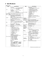
Page 11: ...11 4 Specifications ...

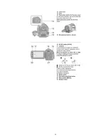
Page 12: ...12 5 Location of Controls and Components Followings are the Location of Controls and Components for SDR S50P PC T50P PC T55P PC as a sample For other models refer to each Operating Instructions ...

Page 13: ...13 ...

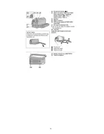
Page 14: ...14 ...

Page 15: ...p screen of the service menu Push the menu button to end the service mode and then POWER OFF Screen display Contents Function 1 Factory settings Function to throw a product up in a factory shipment state 3 Self check execution Function to check self as for the state of eSD 4 Lock search history indication Display an error code for three histories saved in EEPROM 5 Power ON self check result dis pl...

Page 16: ...istory Indication 1 Select 4 Lock search history indication Operation specifications Indication contents Lock search history indication Display the camera system error code for three histories saved in EEPROM The error code contents which are displayed Lock search history indication is finished by POWER OFF Error code Function 51 Focus control is abnormal 52 Zoom control is abnormal 53 OIS lens co...

Page 17: ...ing communication test result CAM PWR Communication test between IC2304 to IC2006 CAM UNI Communication test between IC3401 to IC2006 Display other than OK are abnormalities of each lines Power ON self check result display is finished by POWER OFF 6 4 Lock Search History Clear 1 Select 10 Lock Search History Clear Operation specifications Lock Search History Clear An error code for three histories...

Page 18: ...18 7 Service Fixture Tools 7 1 Service Tools and Equipment ...

Page 19: ...y Instructions 8 1 Disassembly Flow Chart This flow chart indicates the disassembly steps the cabinet parts and P C B Unit in order to access to be serviced When reinstalling perform the steps in the reverse order 8 2 P C B Layout ...

Page 20: ...t LED Light P C B SDR T51 T56 Fig D13 3 Screws J 1 Screw SDR T51 T56 Shutter Unit LED Light P C B SDR T51 T56 Fig D14 4 Tabs Shutter Cover Shutter Panel Fig D15 Mic Unit 7 Main P C B ESD P C B SDR T50 T51 T55 T56 Fig D16 1 Screw K 3 Screws L Side L Angle Fig D17 4 Connectors FP6001 FP6004 FP6007 FP6008 1 Screw M Main Frame Fig D18 4 Screws N 2 Screws SDR T50 T51 T55 T56 Main P C B 1 Connector FP60...

Page 21: ...21 Fig D3 Fig D4 ...

Page 22: ...22 Fig D5 Fig D6 Fig D7 Note for attaching Top Operation Unit Top Operation Unit is installed and the following wire rod is a thing that becomes like Fig D8 Fig D8 ...

Page 23: ...23 Fig D9 Note for attaching Speaker Angle Make sure that speaker wire is under Speaker Angle Fig D10 Fig D11 Fig D12 ...

Page 24: ...24 Fig D13 Fig D14 Fig D15 Fig D16 ...

Page 25: ...25 Fig D17 Fig D18 Fig D19 Fig D20 ...

Page 26: ...26 Fig D21 Fig D22 ...

Page 27: ... Unit The following flowchart describes order or steps for removing the Camera lens unit and certain printed circuit boards in order to make access to the item needing service To reassemble the unit follow the steps in reverse order Fig L1 Fig L2 ...

Page 28: ...28 8 4 1 How to use of CCD positioning pin RFKZ0476 ...

Page 29: ...ure consult the Adjustment Manual which is available in Adjustment software The adjustment instruction is available at Software download on the Support Information from NWBG VDBG AVC web site in TSN System 9 2 Service Positions 9 2 1 List of the extension cables Use the following extension cables when checking or adjusting individual circuit boards except module Parts Main P C B ...

Page 30: ...30 9 2 2 Checking and repairing individual circuit boards How to use extension cables ...

Page 31: ...31 9 3 Location for Connectors of the Main P C B 9 3 1 Main P C B ...

Page 32: ...ment jig as follows 9 4 1 Adjustment Procedure Connect the main unit to PC with USB The adjustment instruction is available at Software download on the Support Information from NWBG VDBG AVC web site in TSN System Figure of connection Figure of Image when adjustment Part Number of jig Only a necessary jig mentions it setup electric adjustment Ref Parts Name Parts No Q ty Remarks 1 Personal Compute...

Page 33: ... manual for SD Video Camera 1 Installation of USB SERIAL Driver Execute the Setup exe file in Com Mass folder by double clicking to install the USB SERIAL driver 2 Set Up a Remove the SD card from this unit b While keep pressing the iA button and DEL button hold left the zoom lever towards to W position for more than 3 seconds until the COM is displayed on LCD 3 Release of COM mode It is necessary...

Page 34: ...CD Panel with your hand When cleaning the lens use air Blower to blow off the dust When cleaning the LCD Panel dampen the lens cleaning paper with lens cleaner and the gently wipe the their surface Note A lens cleaning paper and lens cleaner are available at local camera shops and market place ...

Page 35: ...s the center of joystick button 5 After few seconds END is displayed on LCD monitor Cutting of battery connection or AC power supply connection as a com pletion of the FACTORY SETTINGS 11 2 What is the factory settings The factory settings clean up and or refresh the following settings 1 MENU MODE ADJUSTMENT VALUE 2 SD card format 3 Reset the folder number and file number of still pictures Setting...

Page 36: ...Gray Type SDR S50EB N Gold Type SDR S50P PC EG EP EE GC GA T50GC GA GK T51PU PR T55P GK SDR T50P SDR T50PC SDR T50EG SDR T50EF SDR T50EC SDR T50EP SDR T50EB SDR T50EE SDR T50GC SDR T50GA SDR T50GK SDR T51PU SDR T51PR SDR T55P SDR T55PC SDR T55EB SDR T55GC SDR T55GA SDR T55GK SDR T56PU SDR S50P SDR S50PC SDR S50EG SDR S50EF SDR S50EC SDR S50EP SDR S50EB SDR S50EE SDR S50GC SDR S50GA SDR S50GN SDR S...

Page 37: ...y exist some errors in the voltage values depending on the internal impedance of the DC circuit tester REF No PIN No REC PB EE IC3901 1 1 4 1 4 1 4 IC3901 2 0 0 0 IC3901 3 3 3 3 IC3901 4 1 4 1 4 1 4 IC3902 1 1 4 1 4 1 4 IC3902 2 0 0 0 IC3902 3 3 3 3 IC3902 4 1 4 1 4 1 4 Q3901 E 3 1 3 1 3 1 Q3901 C 0 0 0 Q3901 B 3 1 3 1 3 1 S2 2 Monitor P C B REF No PIN No REC PB EE Q901 E 1 4 1 4 1 4 Q901 C 0 0 0 ...

Page 38: ...PLY CONTROL CIRCUIT USB TERMINAL IC1001 POWER SUPPLY Q6402 6403 LED DRIVE IC601 CONTROLLER SIGNAL PROCESSOR IC3402 FLASH MEMORY LCD 2 7 WIDE IC3401 VIDEO SIGNAL PROCESS AUDIO SIGNAL PROCESS MICROCONTROLLER INTERFACE ATAPI INTERFACE SD CARD INTERFACE USB INTERFACE MEMORY INTERFACE DAC VCO JPEG COMPRESSION ETC AV MULTI JACK AV OUTPUT REAR P C B TG AFE IC101 TG AFE IC3901 IC3902 GYRO SENSOR LED LIGHT...

Page 39: ...ION UNIT GND ZOOMAD AVREF AVREF VTR_KEY_4 GND GND ZOOMAD AVREF AVREF VTR_KEY_4 GND 1 2 3 4 5 6 7 8 9 10 11 12 13 14 17 16 15 18 19 22 21 20 18 17 16 15 14 13 12 11 10 9 6 7 8 5 4 1 2 3 1 2 5 4 3 6 7 10 9 8 10 9 6 7 8 5 4 1 2 3 FP6701 22 21 23 24 25 26 27 28 29 30 31 32 33 34 35 36 37 38 39 40 20 19 18 17 16 15 14 13 12 11 10 9 6 7 8 5 4 1 2 3 SPOUT1 SPOUT2 BATT_ BATT_ BATT_ BATT_ BATT_ BATT_ BATT_...

Page 40: ...C100MA0410 Q3901 B1ADKB000015 1 9 7 5 3 2 4 6 8 22 14 11 12 10 13 19 18 21 20 15 17 16 G1 G2 K1MN22BA0197 FP3901 G_GYRO_REFY G_GYRO_REFY G_GYRO_REFP G_GYRO_REFP G_GYROP G_GYROP G_GYROY G_GYROY BUS24_SDTA1 BUS24_SDTA1 PW_SD3R2VCAR BUS24_SDTA2C BUS24_SDTA2 BUS24_SDTA2 CLK24_SDTA3C BUS24_SDTA3 BUS24_SDTA3 CLK24_SDCMDA CLK24_SDCMDA BUS24_SDCMDC BUS24_SDTA0 BUS24_SDTA0 BUS24_SDTA0C BUS24_SDTA1C CLK49_S...

Page 41: ...1 TH201 B1ABBB000028 Q201 H2 H1 7R5V SUB RESET 12V THERMO GND GND GND GND CCDOUT V1 V2 V3 V4 V5 V6 0 5mm D4CC11030013 K1MN18A00064 CONNECT TO RL4803 RL4804 RL4802 RL4801 1 6 4 2 3 5 FT4801 M4802 WM 58A112A M4801 WM 58A112A GND GND ECM R ECM R ECM R ECM L ECM L ECM L 0 5mm L 0 1 L 0 1 TO MAIN L 0 2 K1MN06B00146 SDR T55 T56 T51 T50 S50 EMC Schematic Diagram SDR T55 T56 T51 T50 S50 CCD Schematic Diag...

Page 42: ... B E_T E_D GND_ADP_ PW_ADP_ BATT_ BATT_ BATT_ BATT_ BATT_ BATT_ BATT_ BATT_ BATT_ BATT_ BATT_ BATT_ BATT_ BATT_ BATT_ BATT_ T T D D BATTERY CATCHER POWER RED RED STANDBY GREEN DISK_ACCESS_LED DISK_ACCESS_LED S 0 2 L 0 2 L 0 2 L 0 2 L 0 2 L 0 2 L 0 2 L 0 2 L 0 2 L 0 2 AVREF AVREF GND GND VTR_KEY_4 ZOOMAD SS_SW TO K1KA40BA0052 TO MAIN MOVING_PICTURE_REC PLAY TO OP SPOUT1 SPOUT1 SPOUT2 SPOUT2 N C DC ...

Page 43: ...197 TO MONITOR FP6001 K1MN27AA0094 TO MAIN L 1 025 LCD_BL_K LCD_BL_K LCD_BL_A LCD_BL_A LCD_COM LCD_COM LCD_VST LCD_VST LCD_HCK1 LCD_HCK1 LCD_8R5V LCD_8R5V LCD_PSIG LCD_PSIG LCD_G LCD_G LCD_R LCD_R LCD_B LCD_B LCD_R L LCD_R L REGD3V REGD3V LIBATT LIBATT ADKEY3 ADKEY3 ADKEY2 ADKEY2 L 0 1 L 0 1 L 0 25 LCD_VCK LCD_VCK LCD_EN LCD_EN LCD_HST LCD_HST LCD_HCK2 LCD_HCK2 LCD_RVS LCD_DWN LCD_DWN LCD_WIDE LCD...

Page 44: ...2 10 13 19 18 21 20 15 17 16 G1 G2 FP902 K1MN24BA0197 B0BC5R6A0266 D906 D905 B0BC016A0267 DSA300100L Q901 DSA300100L Q902 B901 ML 614S DN G_LCD_G_L2 G_LCD_B_L2 G_LCD_B_L1 G_LCD_G_L1 G_LCD_R_L2 G_LCD_R_L1 CLK3_HCK1_L1 CLK3_HCK2_L1 PW_BATT_L2 PW_LCD_BL_A PW_LCD_BL_K PW_BATT_L1 PW_REGD3V PW_8R5V_L1 R REF HST NRW1 HCK2 TEST1 PCG G B RGT PSIG HCK1 TEST2 TO SONY LCD PANEL VST VCK COM1 CS VSSG NRW2 XSTBY...

Page 45: ... NU T14 RFU U1 RFU T2 RFU T1 RFU T5 RFU T3 NU R14 NU T13 NU T12 VDD T10 P3 RFU 88 RFU R3 VDD U9 NU U12 RFU U10 RFU U6 VSS U8 RFU U7 J7 RFU J6 RFU J9 RFU J8 RFU J3 RFU J5 RFU J4 RFU J12 RFU J10 RFU J11 RFU K1 RFU K3 RFU J14 NU K4 VSS K6 VDD K5 RFU J13 RFU K2 VDDC 43 RFU K7 N12 NU N13 NU M13 NU N1 RFU M14 NU M7 VSS M8 RFU L4 NC M5 RFU M6 VDD M12 NU M9 RFU M2 RFU K14 NU L12 NU L3 RFU M1 RFU L13 NU L1...

Page 46: ...01 Q3901 R3901 R3902 R3903 R3904 R3905 R3906 R3907 R3908 R3909 R3910 R3911 R3912 R3913 R3914 R3915 R3916 R3917 R3918 RL3901 RL3902 MK7 MK8 MK6 MK5 4 3 13 11 10 12 8 7 6 5 4 3 2 1 9 14 HS3901 Q201 TH201 R202 R201 C202 C201 FT201 MK1 MK2 Foil Side 20 15 11 10 5 1 IC201 Component Side SDR T55 T56 T51 T50 S50 Rear P C B 10 9 8 7 6 5 4 3 2 1 G F E D C B A Foil Side Component Side SDR T55 T56 T51 T50 S5...

Page 47: ...35 21 20 5 1 30 10 25 15 FP6701 2 1 P6702 RL6701 S6701 4 3 2 1 S6702 MK3 MK2 MK5 MK1 R6702 R6703 R6701 LB6701 5 1 6 FP6703 LB6702 3 2 1 JK6702 1 4 2 3 JK6701 SDR T55 T56 T51 T50 S50 EMC FPC P C B SDR T55 T56 T51 T50 S50 DC BATT OP FPC P C B 10 9 8 7 6 5 4 3 2 1 G F E D C B A Foil Side Component Side Foil Side ...

Page 48: ...S 13 ...

Page 49: ...S 14 S5 5 MONI FPC P C B FT901 1 2 S601 1 4 N M L K J I H G F E D SDR T55 T56 T51 T50 S50 MONI FPC P C B S 14 ...

Page 50: ...S 15 2 4 SDR T55 T56 T51 T50 S50 MONI FPC P C B ...

Page 51: ...S 16 FT901 1 2 S601 FT6001 SDR T55 T56 T51 T50 S50 MONI FPC P C B 11 10 9 8 7 6 5 4 3 2 1 L K J I H G F E D C B A 3 4 Foil Side ...

Page 52: ...S 17 4 4 21 20 19 18 17 16 15 14 13 12 11 SDR T55 T56 T51 T50 S50 MONI FPC P C B ...

Page 53: ...10 5 1 20 25 26 FP901 15 10 5 1 20 24 FP902 5 1 6 FP903 e Q901 e Q902 R903 R904 R905 R906 R907 R908 R909 R910 R911 R912 R913 R914 R915 R916 R917 R918 MK6 MK5 MK8 MK7 D901 D902 D903 D904 4 3 2 1 S901 4 3 2 1 S902 SDR T55 T56 T51 T50 S50 Monitor P C B 10 9 8 7 6 5 4 3 2 1 G F E D C B A Foil Side Component Side ...

Page 54: ... 124 123 122 121 120 119 118 117 116 115 114 113 112 111 110 109 108 107 106 105 104 103 102 101 100 99 98 97 96 95 94 93 92 91 90 89 88 87 86 85 84 83 82 81 80 79 78 77 76 75 74 73 72 71 70 69 68 67 66 65 64 63 62 61 60 59 58 57 56 55 54 53 52 51 50 49 48 47 46 45 44 43 42 41 40 39 38 37 36 35 34 33 32 31 30 29 28 27 26 25 24 23 22 21 20 19 18 17 16 15 14 13 12 11 10 9 8 7 6 5 4 3 2 1 IC3201 C321...

Page 55: ...S 20 ...

Page 56: ...this list 2 IMPORTANT SAFETY NOTICE Components identified with the mark have the special characteristics for safety When replacing any of these components use only the same type 3 Unless otherwise specified All resistors are in OHMS K 1 000 OHMS All capacitors are in MICRO FARADS uf P uuF 4 The marking RTL indicates the retention time is limited for this item After the discontinuation of this asse...

Page 57: ...C3902 L2ES00000019 IC 1 E S D R906 D0GB222JA041 M RESISTOR CH 1 10W 2 2K 1 R907 D0GB103JA057 M RESISTOR CH 1 10W 10K 1 L3901 G1C100MA0410 CHIP INDUCTOR 10UH 1 R908 D0GB272JA041 M RESISTOR CH 1 10W 2 7K 1 R909 D0GB103JA057 M RESISTOR CH 1 10W 10K 1 Q3901 B1ADKB000015 TRANSISTOR 1 E S D R910 D0GB272JA041 M RESISTOR CH 1 10W 2 7K 1 R911 D0GB562JA041 M RESISTOR CH 1 10W 5 6K 1 R3902 ERJ2GEJ220 M RESIS...

Page 58: ...EC B36 XQN16 BJ5FJK SCREW 1 RTL E S D B37 XQN16 BJ4FN SCREW 1 22 VEP03H83CQ MAIN P C B 1 S50EE GC GN GA B38 XQN16 BJ4FN SCREW 1 RTL E S D B39 XQN16 BJ4FN SCREW 1 22 VEP03H83CN MAIN P C B 1 S50P PC PU PR B40 XQN16 BJ4FN SCREW 1 RTL E S D B41 XQN16 B4FN SCREW 1 23 LSKM1999 REAR CASE 1 B42 XQN16 B4FN SCREW 1 24 LSGT0630 BATTERY RELEASE KNOB 1 B43 XQN16 B4FN SCREW 1 25 LSMB0369 BATTERY RELEASE SPRING ...

Page 59: ...CASE A U 1 W T50GC GK GA 34 LSYK2997 LCD CASE A U 1 K T51PU PR 34 LSYK2998 LCD CASE A U 1 N T51PU PR 34 LSYK2999 LCD CASE A U 1 T51PU R 34 LSYK3000 LCD CASE A U 1 T51PU P 34 LSYK2886 LCD CASE A U 1 K T55EB P PC GC GA 34 LSYK2887 LCD CASE A U 1 N T55P GK 34 LSYK2888 LCD CASE A U 1 T55P A 34 LSYK2889 LCD CASE A U 1 T55GK P 34 LSYK2890 LCD CASE A U 1 T55GK W 34 LSYK3001 LCD CASE A U 1 T56PU K 34 LSYK...

Page 60: ...T 1 401 2 L6HA66NB0012 FOCUS MOTOR UNIT 1 401 3 LSEM0118 AUTO IRIS U 1 402 VEP22409A CCD P C B 1 403 LSDW0141 CCD CASE 1 404 LSFL0343 OPTICAL LPF 1 405 LSMX0246 CCD CUSHION 1 B401 LSHD0136 SCREW 1 B402 LSHD0136 SCREW 1 B403 XQN16 BJ4FN SCREW 1 B404 XQN16 BJ4FN SCREW 1 B405 XQN16 BJ4FN SCREW 1 B406 XQN16 BJ4FN SCREW 1 B407 XQN16 BJ4FN SCREW 1 B408 XQN16 BJ4FN SCREW 1 S 25 ...

Page 61: ...CASE U 1 P T55GK 510 VQT2L31 O I 1 T50GA T55GA S50GA 501 VYQ5321 PACKING CASE U 1 W T55GK ENGLISH 501 VPG2K17 PACKING CASE U 1 K T56PU CHINESE TRADITIONAL 501 VPG2D83 PACKING CASE U 1 K S50EG EP EF EB EC EE 510 VQT2L32 O I 1 T50GA T55GA S50GA GN GA THAI HINDI 501 VYQ5297 PACKING CASE U 1 N S50EG EP EE GA 510 VQT2L16 O I 1 T51PU T56PU S50PU 501 VYQ5301 PACKING CASE U 1 R S50EG EP EF EB EC EE ENGLIS...

Page 62: ...31 56 35 43 22 51 B20 B19 B18 42 50 B47 B46 B8 B44 B36 B41 B43 B42 1 B23 B33 B11 14 10 B2 11 12 B10 B13 B14 B15 B16 B9 36 37 38 39 27 32 B21 B24 B22 28 29 B12 30 2 31 24 23 B7 45 9 8 54 3 7 T51 T56 4 5 6 48 44 46 47 49 B35 B34 B5 B4 B6 25 26 B25 B39 B37 B40 40 41 B38 B45 ...

Page 63: ...S7 2 LCD Section S 28 15 17 16 18 34 19 20 21 33 B17 B26 B27 ...

Page 64: ...S7 3 Lens Section S 29 Lubrication Points Lubrication Points 401 401 1 401 3 401 2 403 404 405 402 B401 B402 B408 B407 B404 B405 B406 B403 ...

Page 65: ...S7 4 Packing Parts and Accessories Section S 30 503 GN 506 EB GC GA EC EE EF EG EP GC PR GA GK P PC PU 506 506 506 506 509 502 501 508 504 505 510 511 Battery Pack 507 ...

Reviews: