background image

18

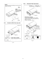
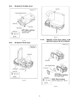
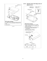
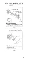
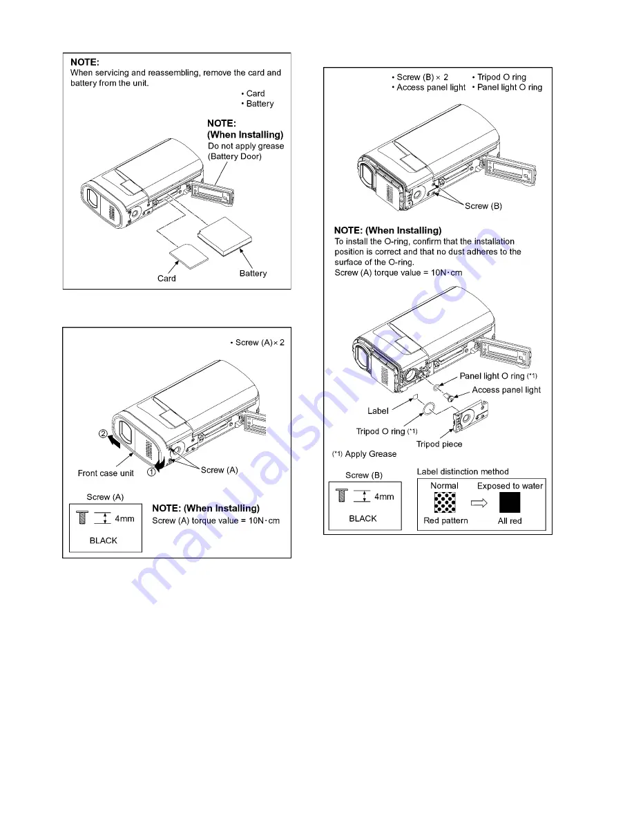
8.3.1.

Removal of the Front case unit

Fig. D1

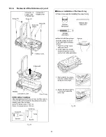
8.3.2.

Removal of the Tripod piece 

Fig. D2

Summary of Contents for SDR-SW20E

Page 1: ...orized copying and distribu tion is a violation of law ORDER NO VM0801003CE B27 SD Video Camera Model No SDR SW20P SDR SW20PC SDR SW20PL SDR SW20E SDR SW20EB SDR SW20EE SDR SW20EF SDR SW20EG SDR SW20EP SDR SW20GC SDR SW20GN SDR SW28GK Vol 1 Colour S Silver Type R Red Type ...

Page 2: ... About Lead Free Solder PbF 7 3 3 Important Notice 1 Other than U S A and Canadian Market 7 3 4 How to Define the Model Suffix NTSC or PAL model 8 4 Specifications 9 5 Location of Controls and Components 11 6 Service Mode 12 6 1 Lock Search History Indication 13 7 Service Fixture Tools 14 7 1 When Replacing the Main PCB 14 7 2 Service Position 14 8 Disassembly and Assembly Instructions 15 8 1 Disa...

Page 3: ...exposed to shock hazards 1 2 Leakage Current Cold Check 1 Unplug the AC cord and connect a jumper between the two prongs on the plug 2 Measure the resistance value with an ohmmeter between the jumpered AC plug and each exposed metal lic cabinet part on the equipment such as screwheads connectors control shafts etc When the exposed metal lic part has a return path to the chassis the reading should ...

Page 4: ...ly a grounded tip soldering iron to solder or unsolder ES devices 4 Use only an antistatic solder removal device Some solder removal devices not classified as antistatic ESD protected can generate electrical charge sufficient to damage ES devices 5 Do not use freon propelled chemicals These can generate electrical charges sufficient to damage ES devices 6 Do not remove a replacement ES device from...

Page 5: ...must not be used until a replacement cover is obtained A replacement fuse cover can be purchased from your local Panasonic Dealer If the fitted moulded plug is unsuitable for the socket outlet in your home then the fuse should be removed and the plug cut off and disposed of safety There is a danger of severe electrical shock if the cut off plug is inserted into any 13 ampere socket If a new plug i...

Page 6: ... be subjected to excessive heat or discharge It must therefore only be fitted in requirement designed specifically for its use Replacement batteries must be of same type and manufacture They must be fitted in the same manner and location as the original battery with the correct polarity contacts observed Do not attempt to re charge the old battery or re use it for any other purpose It should be di...

Page 7: ... Remove the remaining lead free solder on the PCB cleanly for soldering of the new IC Since the melting point of the lead free solder is higher than that of the normal lead solder it takes the longer time to melt the lead free solder Use the soldering iron more than 70W equipped with the temperature control after setting the temperature at 350 30 C 662 86 F Recommended Lead Free Solder Service Par...

Page 8: ...TIAL SETTING data which is stored in Flash ROM mounted on Main PCB 3 4 1 Defining methods To define the model suffix to be serviced refer to the rating label which is putted on the bottom side of the Unit NOTE After replacing the MAIN PCB be sure to achieve adjustment The adjustment instruction is available at software download on the Support Information from NWBG VDBG PAVC web site in TSN system ...

Page 9: ...9 4 Specifications For P PC PL areas For other areas ...

Page 10: ...10 ...

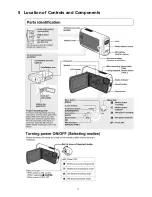
Page 11: ...11 5 Location of Controls and Components ...

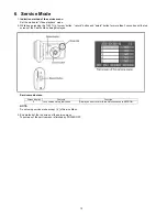
Page 12: ...more than 3 seconds until the top screen of the Service Menu being displayed Service mode menu NOTE Do not using service mode except 4 of Service Menu 3 End method of the top screen of the service menu Top screen of the service menu is finished by POWER OFF Screen display Contents Function 4 Lock search history indication Display an error cord for three histories saved in EEPROM ...

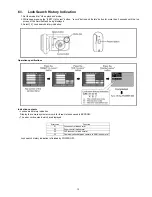
Page 13: ...ect 4 Lock search history indication Operation specifications Indication contents Lock search history indication Display the camera system error cord for three histories saved in EEPROM The error cord contents which are displayed Lock search history indication is finished by POWER OFF Error code Function 51 Focus control is abnormal 52 Zoom control is abnormal 53 OIS lens control is abnormal 33 Co...

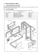
Page 14: ...ervice Position is used for checking and replacing parts Use the following Extension cables for servicing Table S1 Extension Cable List No Parts No Connection Form 1 VFK1364 FP6931 MAIN CCD UNIT 14PIN 0 5 FFC 2 VFK1461 FP6971 MAIN LENS UNIT 20PIN 0 5 FFC 3 VFK1388 FP6902 MAIN FP4802 FRONT 12PIN 0 5 FFC 4 VFK1716 FP6903 MAIN FP8101 MONITOR 25PIN 0 3 FFC 5 VFK1461 FP6905 MAIN BATTERY CHATCER UNIT 20...

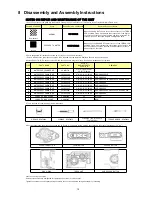
Page 15: ...㪅㩷㪥㪦㪅 㩿㪚㪘㪙㪠㪥㪜㪫㩷㪧㪘㪩㪫㪪 㪣㪦㪚㪘㪫㪠㪦㪥㪀 㪩㪜㪤㪘㪩㪢㪪 㪘 㪮㪘㪫㪜㪩㪧㪩㪦㪦㪝㩷㪩㪬㪙㪙㪜㪩㩷㪢㪠㪫 㪭㪬㪤㪞㪈㪎㪐㪈 㪊㪆㪎㪄㪈㪇㪆㪈㪌㪆㪊㪋㪄㪊㪎㪆㪌㪋㪆 㪌㪍㪆㪎㪉㪆㪎㪌㪆㪏㪊㪆㪏㪐 㪙 㪮㪘㪫㪜㪩㪧㪩㪦㪦㪝㩷㪚㪘㪙㪠㪥㪜㪫㩷㪢㪠㪫 㪭㪬㪰㪢㪉㪡㪊㪇㪘 㪉㪆㪈㪉㪆㪋㪏㪆㪌㪈㪆㪌㪊㪆㪏㪇㪆㪏㪍 㪪㪛㪩㪄㪪㪮㪉㪇㩷㪧㪩㪃㪧㪣㪩㩷 㪙 㪮㪘㪫㪜㪩㪧㪩㪦㪦㪝㩷㪚㪘㪙㪠㪥㪜㪫㩷㪢㪠㪫 㪭㪬㪰㪢㪉㪡㪊㪇㪙 㪉㪆㪈㪉㪆㪋㪏㪆㪌㪈㪆㪌㪊㪆㪏㪇㪆㪏㪍 㪪㪛㪩㪄㪪㪮㪉㪇㩷㪧㪚㪩㩷 㪙 㪮㪘㪫㪜㪩㪧㪩㪦㪦㪝㩷㪚㪘㪙㪠㪥㪜㪫㩷㪢㪠㪫 㪭㪬㪰㪢㪉㪡㪊㪇㪚 㪉㪆㪈㪉㪆㪋㪏㪆㪌㪈㪆㪌㪊㪆㪏㪇㪆㪏㪍 㪪㪛㪩㪄㪪㪮㪉㪇㩷㪜㪞㪩㪃㪜㪩㪃㪜㪙㪩㪃㪜㪝㪩㪃㪜㪧㪩㪃㪞㪚㪩㪃㪞㪥㪩㪃㪜㪜㪩㩷 㪙 㪮㪘㪫㪜㪩㪧㪩㪦㪦㪝㩷㪚㪘㪙㪠㪥㪜㪫㩷㪢㪠㪫 㪭㪬㪰㪢㪉㪡㪊㪇㪛 㪉㪆㪈㪉㪆㪋㪏㪆㪌㪈㪆㪌㪊㪆㪏㪇㪆㪏㪍 㪪...

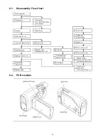
Page 16: ...16 8 1 Disassembly Flow Chart 8 2 PCB Location ...

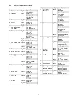
Page 17: ...P C B Fig D18 1 Screw N 2 Ribs FP4801 Flex Front P C B 14 LCD unit Fig D19 R base rubber 4 Screw N Fig D20 GND O ring LCD unit 15 LCD hinge unit Monitor P C B Fig D21 4 Screws P Packing angle 4 screw O rings 2 Screws Q Fig D22 2 Locking tabs LCD case top FP8101 Flex 3 Locking tabs FP8102 Flex LCD hinge unit Monitor P C B 16 LCD panel Fig D23 Reflection sheet Lighting plate Diffusion sheet Prism sh...

Page 18: ...18 8 3 1 Removal of the Front case unit Fig D1 8 3 2 Removal of the Tripod piece Fig D2 ...

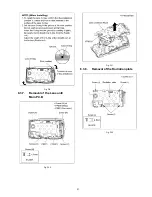
Page 19: ...19 8 3 3 Removal of the Rear cover Fig D3 8 3 4 Removal of the R cover Fig D4 Fig D5 8 3 5 Removal of the Lens piece Lens protection glass and Lens damper Fig D6 ...

Page 20: ...20 8 3 6 Removal of the Side case L unit Fig D7 Fig D8 ...

Page 21: ...21 Fig D9 8 3 7 Removal of the Lens unit Main P C B Fig D10 Fig D11 8 3 8 Removal of the Radiation plate Fig D12 ...

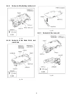
Page 22: ...22 8 3 9 Removal of the Battery catcher unit Fig D13 8 3 10 Removal of the Main P C B and Jack P C B Fig D14 Fig D15 8 3 11 Removal of the Lens unit Fig D16 ...

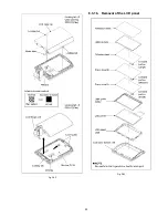
Page 23: ...23 8 3 12 Removal of the Battery case Fig D17 8 3 13 Removal of the Front P C B Fig D18 8 3 14 Removal of the LCD unit Fig D19 ...

Page 24: ...24 Fig D20 8 3 15 Removal of the LCD hinge unit and Monitor P C B Fig D21 ...

Page 25: ...25 Fig D22 8 3 16 Removal of the LCD panel Fig D23 ...

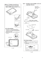
Page 26: ...26 Fig D24 8 3 17 Removal of the Speaker unit and Operation FPC unit Fig D25 ...

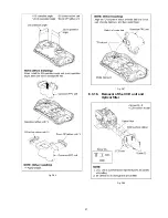
Page 27: ...27 Fig D26 Fig D27 8 3 18 Removal of the CCD unit and Optical filter Fig D28 ...

Page 28: ...28 8 3 19 Removal of the IRIS unit Fig D29 Fig D30 8 3 20 Removal of the Zoom motor unit Fig D31 8 3 21 Removal of the Focus motor unit Fig D32 ...

Page 29: ...29 8 3 22 Removal of the Master flange 4th moving frame unit and 3rd moving frame unit Fig D33 8 3 23 Removal of the Guide pole S Guide pole and 2nd moving frame unit Fig D34 ...

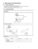
Page 30: ... method of the main unit and an exclusive adjustment jig as follows 9 1 1 Adjustment Procedure Connect the main unit to PC with USB The adjustment instruction is available at Software download on the Support Information from NWBG VDBG PAVC web site in TSN System Figure of connection Figure of image when adjustment Part Number of jig Only a necessary jig mentions it in setup of electric adjustment ...

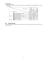
Page 31: ...ion is available at Software download on the Support Information from NWBG VDBG PAVC web site in TSN System 9 2 Repair Record Using the applicable items in Repair Maintenance that is newly provided in the adjustment software record the treatment and the date of execution ...

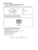
Page 32: ...ted 5 Set the mode dial to the OFF position to close the Factory Setting 10 2 WHAT IS THE FACTORY SETTINGS The factory settings clean up and or refresh the following settings 1 The OSD MENU setting data 2 Deletion only for all scene files in a card and format of the MPEG2 file system area 3 Reset the folder number and file number of still pictures Setting the folder number is 100 and file number i...

Page 33: ...P SDR SW20GC SDR SW20GN SDR SW20EE SDR SW28GK SD Video Camera Name of Signal OFTR FEP This signal is connected to the FEP schematic diagram Circuit name being connected 6 Use the parts number indicated on the Replacement Parts List 7 Indication on Schematic diagrams 5 The voltage being indicated here may be include observational error deviation due to internal resistance and or reactance of equipm...

Page 34: ...WER ON IC4801 1 3 2 IC4801 2 3 2 IC4801 3 3 2 IC4801 4 0 IC4801 5 3 2 IC4801 6 3 2 IC4801 7 3 2 IC4801 8 6 2 Q4801 E 5 4 Q4801 C 6 2 Q4801 B 6 1 Q6501 E 2 7 Q6501 C 3 7 Q6501 B 0 7 Q6502 E 3 4 Q6502 C 0 Q6502 B 2 7 S2 2 Monitor P C B REF No PIN No POWER ON Q8101 E 0 7 Q8101 C 2 1 Q8101 B 1 6 Q8102 E 0 7 Q8102 C 2 1 Q8102 B 1 6 Q8104 E 0 7 Q8104 C 2 1 Q8104 B 1 6 Q8105 E 0 7 Q8105 C 2 1 Q8105 B 1 6...

Page 35: ... IC701 LENS DRIVE IC303 VERTICAL DRIVER IC302 TG AFE IC3400 MPEG CODEC IC1001 POWER CIRCUIT IC2304 RTC IC6004 EEPROM IC601 LCD CONTROLLER COLOR LCD PANEL 2 7 PANEL IC3401 SDRAM 512Mbit IC3402 FLASH ROM 512Mbit SD CARD USB TERMINAL IC3301 AVIO SPEAKER IC4801 MIC AMP ECM AV S OUT MULTI OPERATION DC JACK BATTERY X6001 6 75MHz FLASH SCOPE LAMP X301 OSC 36MHz CLOCK 12MHz ...

Page 36: ...22 CAM MICOM TMS 23 CAM UART DI 30 31 32 33 D GND D GND D GND TRACEPKT0 34 35 36 TRACEPKT2 TRACEPKT5 TRACEPKT7 37 PIPESTA1 38 D GND 39 EXTRGO0 40 ARMTMS 41 ARMTDI 42 DBGA 43 D GND 44 D GND 45 CAM MICOM TRST 46 CAM MICOM TDO 29 XRST ARM 28 POWER RST 27 RXD 26 CAM MICOM DINT 25 CAM UART DO 24 D GND To SOFT DBG D GND 2 D GND 4 LCD BL 5V 6 LCD COM 8 LCD VCK 10 LCD UD 12 14 16 18 19 17 15 13 11 9 5 3 1...

Page 37: ...NI Y Y REGA5V REGA5V IRDET REGD3V TO MAIN LIBATT A_M_OUT_L A_M_OUT_R TO ECM 3 2 4 G1 G2 JK6352 K2EB2E000009 J0JHC0000018 LB6350 J0JHC0000018 LB6351 LB4004 J0JYC0000061 LB4006 J0JYC0000059 LB4005 J0JYC0000061 LB4001 J0JYC0000061 LB6352 J0JYC0000061 F1H1C105A095 C6354 4700P C4002 C4003 4700P D4ED18R00008 VA6352 D4ED18R00008 VA6351 2 1 K5H4021A0011 IP6351 2 1 R6352 D1JBR102A006 2 1 R6351 D1JBR102A006...

Page 38: ...63 B3AFB0000163 D8105 D8104 B3AFB0000163 D8106 B3AFB0000163 1 8 6 4 2 3 5 7 9 24 25 19 20 18 22 23 21 13 10 12 11 15 17 16 14 FP8101 K1MN25AA0035 L8101 G1C101KA0055 K9ZZ00001073 EP8101 Q8102 2SC6054J0L Q8104 2SC6054J0L Q8105 2SC6054J0L Q8108 2SC6054J0L Q8101 2SC6054J0L PW_L8R5V_LC3 PW_LBL5V G_M_G_1 G_M_R_1 G_M_B_1 CLK3_L_HCK1 CLK3_L_HCK2 PW_L8R5V_LC1 G_M_G G_M_R G_M_B R LCD_BL_5V LCD_BL_5V BL_CONT...

Page 39: ...2 4 6 8 17 18 13 14 11 10 12 16 15 20 19 FT2501 4 1 2 3 D2501 B3ABB0000033 1 3 2 IC2501 B4ZZ00000012 C2506 F1H0J106A009 PW_CPU_VDD PW_RTC3R1V P_PLAY POWER_SW M_PLAY M_REC P_REC LEFT 1 32V 1 32V 1 32V KEY3 0V 0V 0V 0V DELETE 0 62V 0 62V 0 62V 2 10V KEY1 P_ON OPEN P_OFF CLOSE KEY2 MENU 2 1V 2 1V ENTER ZOOM UP DOWN RIGHT RED POWER STANDBY GREEN SS 0 97V WIDE_LOW WIDE_HI TELE_LOW 1 93V GND GND GND GND...

Page 40: ... 16V1 22 2SC393000L Q291 1 8 9 6 4 2 3 5 7 14 12 10 11 13 FT31 11 4 13 14 12 1 2 3 5 6 7 10 8 9 IC291 R R V2 V2 V4 V4 V3 V3 GND GND GND GND V1 V1 SUB SUB 12V H1 H1 H2 H2 7V OUT TEST PT VDD SBSW VOUT TO SUB SDR SW20 Series CCD FPC Schematic Diagram 10 9 8 7 6 5 4 3 2 1 G F E D C B A ...

Page 41: ... Side 1 2 ZB6801 R6801 R4804 MK8 MK7 MK6 MK5 D6504 C4812 C4811 C4803 VA4802 VA4801 RL4801 R6509 R6507 R6506 R6505 R6504 R4811 R4810 R4809 R4808 R4807 R4806 R4805 R4803 R4802 Q6502 Q6501 Q4801 MK4 MK3 MK2 MK1 1 4 5 8 IC4801 10 5 1 12 FP4802 1 4 FP4801 D6503 C6505 C6504 C6503 C4815 C4810 C4809 C4808 C4806 C4805 C4804 C4802 C4801 ...

Page 42: ...C B A Foil Side Component Side VA6352 IP6351 LB6351 MK6 MK5 R6352 R6351 1 2 3 4 5 JK6351 4 3 2 JK6352 C6354 FL6352 MK8 MK7 C4003 LB4006 LB4005 LB4004 LB4001 C4002 10 9 8 7 6 5 4 3 2 1 JK4001 LB6352 VA6351 MK4 MK3 4 3 2 1 FL6351 LB6350 RL6301 MK1 MK2 30 25 20 16 15 10 5 1 FP6001 ...

Page 43: ...S 11 S5 3 Monitor P C B SDR SW20 Series Monitor P C B Component Side 10 9 8 7 6 5 4 3 2 1 G F E D C B A Component Side D8102 D8106 D8105 D8104 D8103 S5 3 1 Monitor P C B Component Side ...

Page 44: ... Foil Side 1 1 EP8101 C8110 C8114 D8113 R8133 C8113 Q8113 R8126 C8112 C8111 R8123 R8116 R8114 C8109 C8108 Q8105 Q8107 Q8108 Q8104 Q8102 Q8101 L8101 15 10 5 1 20 24 FP8102 25 20 15 10 5 2 1 24 FP8101 R8119 R8112 R8110 R8107 R8124 C8105 C8106 C8104 C8107 R8105 R8106 R8102 C8101 D8101 R8135 R8136 C8116 Q8112 R8127 ...

Page 45: ... 1 2 1 S2510 R2555 R2551 R2552 R2554 CL2508 CL2507 CL2506 CL2505 CL2504 CL2503 CL2502 CL2501 C2506 R2522 R2521 R2520 R2518 R2515 R2514 R2513 R2512 R2510 R2509 R2508 R2507 R2506 R2505 R2502 R2501 IC2501 1 2 3 4 D2501 2 1 2 1 S2516 16 15 14 13 12 11 10 9 8 7 6 5 4 3 2 1 S2515 2 1 2 1 S2513 2 1 2 1 S2509 2 1 2 1 S2508 2 1 2 1 S2507 2 1 2 1 S2506 2 1 2 1 S2505 ...

Page 46: ...S 14 S5 5 CCD FPC P C B SDR SW20 Series CCD FPC P C B 10 9 8 7 6 5 4 3 2 1 G F E D C B A Foil Side Component Side 14 13 12 11 10 9 8 7 6 5 4 3 2 1 IC291 FT31 M01 M02 R292 Q291 D291 C295 C294 ...

Page 47: ... of this assembly in production it will no longer be available All resistors are in OHMS K 1 000 OHMS All capacitors are in MICRO FARADS uf P uuF Components identified with the mark have the special characteristics for safety When replacing any of these components use only the same type 2 IMPORTANT SAFETY NOTICE 3 Unless otherwise specified 4 The marking RTL indicates the retention time is limited...

Page 48: ...1 C8105 ECJ1VC1H390J C CAPACITOR CH 50V 39P 1 C4812 F3F0J226A032 T CAPACITOR CH 6 3V 22U 1 C8106 ECJ1VC1H390J C CAPACITOR CH 50V 39P 1 C6503 F1G0J224A004 C CAPACITOR CH 6 3V 0 22U 1 C8107 ECJ1VB1A105K C CAPACITOR CH 10V 1U 1 C6504 F1G1C104A080 C CAPACITOR CH 16V 0 1U 1 C8109 F1J1A475A023 C CAPACITOR CH 10V 4 7U 1 C6505 F1G0J224A004 C CAPACITOR CH 6 3V 0 22U 1 C8110 ECJ1XB1C104K C CAPACITOR CH 16V ...

Page 49: ...73JA057 M RESISTOR CH 1 10W 47K 1 R2502 D0GB473JA057 M RESISTOR CH 1 10W 47K 1 R2505 D0GB473JA057 M RESISTOR CH 1 10W 47K 1 R2506 D0GB473JA057 M RESISTOR CH 1 10W 47K 1 R2507 D0GB103JA057 M RESISTOR CH 1 10W 10K 1 R2508 ERJ3GEYJ272 M RESISTOR CH 1 10W 2 7K 1 R2509 ERJ3GEYJ562 M RESISTOR CH 1 10W 5 6K 1 R2510 D0GB183JA057 M RESISTOR CH 1 10W 18K 1 R2512 D0GB103JA057 M RESISTOR CH 1 10W 10K 1 R2513 ...

Page 50: ...VUYK2J30C WATERPROOF CABINET KIT 1 EGR ER EBR EFR EPR GCR GNR EER 86 VUYK2J30C WATERPROOF CABINET KIT 1 EGR ER EBR EFR EPR GCR GNR EER 48 VUYK2J30D WATERPROOF CABINET KIT 1 GKR 86 VUYK2J30D WATERPROOF CABINET KIT 1 GKR 48 VUYK2J30E WATERPROOF CABINET KIT 1 PS PLS 86 VUYK2J30E WATERPROOF CABINET KIT 1 PS PLS 48 VUYK2J30F WATERPROOF CABINET KIT 1 PCS 86 VUYK2J30F WATERPROOF CABINET KIT 1 PCS 48 VUYK...

Page 51: ...EW 1 B38 VHD1986 SCREW 1 B39 VHD1986 SCREW 1 B40 VHD1986 SCREW 1 B41 VHD1986 SCREW 1 B42 VHD1986 SCREW 1 B43 XQN16 BJ45FN SCREW 1 B44 XQN16 BJ45FN SCREW 1 B45 XQN16 BJ45FN SCREW 1 B46 XQN16 BJ45FN SCREW 1 B47 XQN16 BJ45FN SCREW 1 B48 XQN16 BJ45FN SCREW 1 B49 XQN16 BJ45FN SCREW 1 B50 XQN16 BJ45FN SCREW 1 B51 XQN16 BJ45FN SCREW 1 B52 XQN16 BJ45FN SCREW 1 B53 VHD1783 SCREW 1 B54 VHD1783 SCREW 1 B55 V...

Page 52: ...CABINET KIT 1 PS PLS 12 VUYK2J30F WATERPROOF CABINET KIT 1 PCS 12 VUYK2J30G WATERPROOF CABINET KIT 1 EGS ES EBS EFS EPS GCS GNS EES 12 VUYK2J30H WATERPROOF CABINET KIT 1 GKS 13 VKM7338 HINGE COVER TOP 1 S 13 VKM7347 HINGE COVER TOP 1 R 14 VKM7339 HINGE COVER BOTTOM 1 15 VUMG1791 WATERPROOF RUBBER KIT 1 16 VGQ9389 FPC HINGE TAPE 1 17 LSGL0505 LIGHTING PLATE 1 18 VGL1167 REFLECTION SHEET 1 19 VEP291...

Page 53: ...ME UNIT 1 207 VXP2255 4TH MOVING FRAME UNIT 1 208 VMS7296 GUIDE POLE 1 209 VMS7828 GUIDE POLE 1 210 VDW1433 MASTER FLANGE 1 211 L6HA64NC0005 ZOOM MOTOR UNIT 1 212 L6HA64NC0006 FOCUS MOTOR UNIT 1 213 VEK0L05 CCD UNIT 1 P PC PL E S D 213 VEK0L06 CCD UNIT 1 EG E EB EF EP GC GN EE GK E S D 214 VEP22381A CCD FPC 1 B200 XQN16 CJ4FJR SCREW 1 B201 XQN16 CJ4FJR SCREW 1 B202 XQN16 CJ7FJ SCREW 1 B203 XQN16 C...

Page 54: ...1 VQT1M26 OPERATING INSTRUCTIONS FRENCH 1 EG EF 311 VQT1M27 OPERATING INSTRUCTIONS ITALIAN 1 EG 311 VQT1M28 OPERATING INSTRUCTIONS DUTCH 1 EG 311 VQT1M29 OPERATING INSTRUCTIONS TURKISH 1 EG 311 VQT1M30 OPERATING INSTRUCTIONS 1 E 311 VQT1M31 OPERATING INSTRUCTIONS PORTUGUESE 1 E 311 VQT1M32 OPERATING INSTRUCTIONS 1 E 311 VQT1M33 OPERATING INSTRUCTIONS DANISH 1 E 311 VQT1M34 OPERATING INSTRUCTIONS E...

Page 55: ...34 33 28 30 B42 B41 B40 2 37 36 B19 B18 B16 B15 B13 B12 B11 B29 B28 53 54 57 B27 B26 48 B36 B35 B34 70 71 72 55 56 50 49 41 B20 42 47 46 B22 B21 43 45 44 51 B47 B48 B49 76 B50 74 75 78 79 B52 77 B25 B24 63 61 60 B43 B44 B45 B51 B46 58 59 B23 62 39 73 66 B14 B17 29 65 89 88 90 87 91 86 B55 80 83 B54 B53 81 82 85 84 ...

Page 56: ...S7 2 LCD Section S 24 12 B10 11 B9 13 4 14 16 15 19 18 17 22 21 20 92 23 24 25 93 7 5 9 B8 B7 B6 B5 8 6 10 27 26 ...

Page 57: ...S7 3 Lens Section S 25 B209 B208 211 203 B207 B206 B205 207 210 212 B210 B211 B202 B204 B203 206 209 208 204 201 202 B201 B200 200 205 214 213 ...

Page 58: ...S7 4 Packing Parts and Accessories Section S 26 304 305 306 302 312 311 317 303 308 307 301 310 SDR SW20 P PC PL SDR SW28 GK 314 SDR SW20 GN 313 SDR SW20 EB GC 316 SDR SW20 E EG EF EP EE GC ...

Reviews: