background image

Pin 

No.

Mark

I/O  / 

Division

Function

10

LG

I

Coil drive input terminal for 
VG voltage increase 
(connected to power supply)

11

PGND2

GND terminal

12

IOUT

O

Charging signal and 
charging feedback output 
terminal

13

PV 

CC

 2

I

Power supply input terminal

14

REGB

O

Regulator drive signal 
output terminal

15 MSTAT/  

/ ACDET

O

DC jack detection output 
terminal

16 MDATA/ 

 / EMP

I

Power drop detection input 
terminal

17

MLD/  / 

VCNT

I

Regulator voltage switching 
input terminal

18 MCLK/  / 

CHARGE

I

Charging ON/OFF input 
terminal

19

S/P

I

Serial/parallel switching 
input terminal (connected to 
power supply)

20

DV 

DD

I

Power supply input terminal

21

CLK

I

DC/DC converter external 
clock input terminal

22 PREGND

GND terminal

23

AREF

O

Audio reference output 
terminal

24

AVCC

O

Ripple filter output terminal

25

CRP

I

Ripple filter smoothing 
capacitor connection 
terminal

26

RESET

O

Reset detection output 
terminal

27

SOFT

O

Soft start setting output 
terminal  / (connected GND 
through capacitor)

28

EO

O

DC/DC converter error 
amplifier output terminal

29

EI

I

DC/DC converter error 
amplifier input terminal

30

VADJ

O

Output for varying DC/DC 
converter output terminal 
(Not used, open)

38

Summary of Contents for SL-VP48

Page 1: ...rtable Video CD Player SL VP48 SL VP43 SL VP33 Traverse Deck RAE0145Z Mechanism Series Colours S Silver Type N Gold Type Areas GK China GH Hong Kong GCS Asia Latin America Middle Near East Africa and Oceania SPECIFICATIONS 1 ...

Page 2: ...pply DC 4 5V Power consumption SL VP33 Using AC adaptor 4 8W SL VP48 SL VP43 AC adaptotr Audio CDs Anti shock OFF ON 4 8W 5 0W Video CDs 4 8W When rechargeing 5 6W Play time When used in hold mode at 25 C temperature and on flat and stable surface SL VP33 2 Alkaline batteries Audio CDs About 18 hours Video CD About 3 hours Rechargeable batteries P 3GAVT Audio CDs About 9 hours Video CDs About 2 ho...

Page 3: ...271g with batteries 228g without batteries Operational temperature range 0 C 40 C Recharging temperature range 5 C 40 C Note Specifications are subject to change without notice Mass and dimensions are approximate These specifications were measured using the AC adaptor 1 Accessories Stereo earphones 1 pc RFEV334P KS Remote control transmitter 1 pc RAK SL974WK Connection cable 1 pc RJL3X001X15 Batte...

Page 4: ...s Wave length 780nm Maximum output radiation power from pickup 100 W VDE Laserradiation from the pickup lens is safety level but be sure the followings 1 Do not disassemble the optical pickup unit since radiation from exposed laser diode is dangerous 2 Do not adjust the variable resistor on the pickup unit It was already adjusted 3 Do not look at the focus lens using optical instruments 4 Recommen...

Page 5: ... precision construction and must not be subjected to impact excessive vibration or other types of rough handling 2 In order to prevent static electricity damage to the laser diode use a short pin or similar tool to short the optical pickup s flexible circuit boards after they have been disconnected from the main circuit board as shown in Fig 1 3 Handle the flexible circuit boards with care excessi...

Page 6: ...hown in Fig 3 2 Work table grounding Put a conductive material sheet or steel sheet on the area where the traverse deck optical pickup is placed and ground the sheet as shown in Fig 4 Caution The static electricity of your clothes will not be grounded through the wrist strap So take care not to let your clothes touch the traverse deck optical pickup Fig 3 Fig 4 6 ...

Page 7: ... checking the operation of the major printed circuit boards and replacing the main components For reassembly after operation checks or replacement reverse the respective procedures Special reassembly procedures are described only when required 5 1 Checking for the video P C B 5 1 1 Checking for the video P C B A side 7 ...

Page 8: ...8 ...

Page 9: ... Check the video P C B A side as shown below 5 1 2 Checking for the video P C B B side 9 ...

Page 10: ...5 2 Checking for the main P C B 5 2 1 Checking for the main P C B A side Follow the Step 1 Step 7 of item 5 1 1 10 ...

Page 11: ... Check the main P C B A side as shown below 5 2 2 Checking for the main P C B B side Follow the Step 1 Step 6 of item 5 1 1 11 ...

Page 12: ... Check the main P C B B side as shown below 5 3 Replacement for the CD cover ass y LCD and JOG knob Follow the Step 1 Step 5 of item 5 1 1 12 ...

Page 13: ...13 ...

Page 14: ...14 ...

Page 15: ...5 4 Replacement for the traverse motor Follow the Step 1 Step 5 of item 5 1 1 15 ...

Page 16: ...5 5 Replacement for the optical pickup Follow the Step 1 Step 5 of item 5 1 1 16 ...

Page 17: ... Follow the Step 1 Step 5 of item 5 4 17 ...

Page 18: ...mally movements of traverse deck touching failure of REST det SW and coming off or cutting off the flexible P C B It is necessary for confirmation or repair and replacement each parts 7 Checking the Operation Problems on the Traverse Deck Optical Pickup Make sure to follow the procedures below to check the operation problems of the traverse deck optical pickup before replacing it Replace the trave...

Page 19: ...in both the forward and reverse directions Checking Manual Search 1 Play an ordinary musical program disc 2 Press the manual search button to check for smooth manual search operations at either low or high speed in both the forward and reverse directions Checking Playability 1 Play the 0 7 mm black dot and the 0 7 mm wedge on the playability test disc SZZP1054C and verify that no sound skip or noi...

Page 20: ... displays self check function 8 1 How to display automatic adjustment results 1 Relaese the bottom cabinet As for the method of disassembly refer to 5 1 1 Chacking for the video P C B 2 Load the test disc SZZP1054C 3 Place it keeping the disc cover side down on the base 4 Make a short circuit between IC301 pin No 1 and GND as shown in Fig 5 5 Insert the AC adaptor plug into the DC IN jack and then...

Page 21: ...he focus servo circuit is correct check the waveform or voltage 2 the optical pickup returns to the normal state by exchanging the traverse deck Follow the below steps when E 4 is displayed Cause Focus gain FGC is set beyond the limit Check if 1 the waveform or voltage of the focus servo circuit is correct check the waveform or voltage 2 the focus coil of the optical pickup is correct around 15 oh...

Page 22: ...ound marking signal is supplied at normal speed from the memory to the D A converter the residual data si accumulated in then mi emory Ifreaccess to the break point is accomplished before the memory becomes empty apparent playback sound is entirely kept free from breaking even when information pauses due to viration etc It was necessary to use the 16M bit memory for securing theaccumulation time o...

Page 23: ...wire for test points 10 2 Test short land Short circuit the lands of the laser ON OFF switch S201 by soldering them It turns ON position Refer to below Fig 7 or printed circuit board and wiring connectiondiagram for short land location Note Remove the solders from the lands after adjustment 10 3 Adjustment point Notes 1 Please refer to the printed circuit board and wiring connection diagram for te...

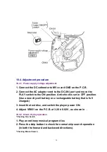
Page 24: ...set in OFF position Use a new dry cell battery or a rechargeable battery that is full charged 3 Insert the test disc and switch the player power ON 4 Adjust VR851 on the P C B at 3 20 0 02V as shown in 10 4 2 Check of play operation Checking Skip Search 1 Play an ordinary musical program disc 2 Press the skip button to check for normal skip search operation in both the forward and backward directi...

Page 25: ...ty test disc SZZP1054C and verify that no sound skip or noise occurs 2 Play the middle tracks of the uneven test disc SZZP1056C and verify that no sound skip or noise occurs 11 Troubleshooting Guide 11 1 Circuit diagram 11 2 Data signal line waveforms Note Use the PVCDD_K06 video CD test disc menu playback feature is available on version 2 0 For color bar display playback the 1st track when the me...

Page 26: ...11 3 Master clock system waveform 11 4 Audio data clock system waveform 11 5 Diagnostic Procedures by Symptom 26 ...

Page 27: ...otate Traverse system focus servo system IC11 supply line clock line system control IC301 Turntable rotates Rotates Traverse system tracking servo system servo system traverse servo system IC101 IC501 IC11 Audio normal Audio normal Video NG IC1000 Audio normal No sound Video NG IC1000 TOC OK counter OK but no sound TOC OK counter OK but no sound and video NG CD disc other than DV Karaoke soft CD a...

Page 28: ...28 ...

Page 29: ...29 ...

Page 30: ...12 Schematic Diagram Note 12 1 Type Illustration of IC s Transistors and Diodes 12 2 Schematic Diagram Notes Notes 30 ...

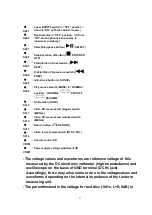
Page 31: ...ME S310 Hold switch HOLD S311 Video CD menu select bigger switch MENU S312 Video CD menu select smaller switch MENU S313 Return button RETURN S314 Video format select switch NTSC PAL VR701 Volume control VR VR851 Power supply voltage adjustment VR The voltage values and waveforms are reference voltage of this measured by the DC electronic voltmeter high impededance and oscilloscope on the basis of...

Page 32: ...y sound capacitors low noise resistor etc are used When replacing any of components be sure to use only manufacture s specified partsshown in the parts list Cautions IC and LSI are sensitive to static electricity Secondary trouble can be prevented by taking care during repair Cover the parts boxes made of plastics with aluminum foil Ground the soldering iron Put a conductive mat on the work table ...

Page 33: ...n input terminal 12 BDO O Dropout signal output terminal H dropout 13 LDON I APC control input terminal 14 GND Connected to GND 15 RFDET O RF detection signal output terminal L detection 16 PDOWN O Reduced voltage detection signal output terminal 17 OFTR O Off track signal output terminal H off track 18 NC Not used open 19 ENV O RF envelop signal output terminal 20 ENV OFF I Envelop control input ...

Page 34: ... clock signal output 11 HDIO I O Adress data input output 12 HSEL O Serial data signal output 13 14 NC Not used open 15 SSYNC I Sync clock signal input 16 HINT I Soft interrupt signal input 17 NC Not used open 18 MCLK O Command clock signal output 19 MDATA O Command data output 20 STAT I Status signal input 21 BLKCK I Sub code block clock input 22 WLSRCN I Remote control signal input 23 NC Not use...

Page 35: ...ery voltage detect signal output 47 CHGCMP I Battery voltage detect signal input 48 MUTEO O Muting signal output 49 50 NC Not used open 51 MLD O Command load signal output 52 RSTAT Not used open 53 CHARGE Not used open 54 VCDRST O VCD reset signal output 55 62 NC Not used open 63 PDOWN I Power down signal input 64 KPOWER O Power supply control output 65 M1 O Microphone volume signal output 66 M0 6...

Page 36: ...terminal 4 FI1 I Focus coil drive signal input terminal 5 RI1 I Focus coil drive signal input terminal 6 RO1 O Focus coil drive signal output terminal 7 PGND1 GND terminal 8 FO1 O Focus coil drive signal output terminal 9 FO2 O Tracking coil drive signal output terminal 10 PGND2 GND terminal 11 RO2 O Tracking coil drive signal output terminal 12 RI2 I Tracking coil drive signal input terminal 13 F...

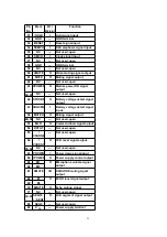
Page 37: ...rse motor drive signal input terminal 30 PC I Hard mute input terminal 31 AC I Power supply input terminal 32 PV CC 4 I Power supply input terminal 16 4 IC11 RS10003E2 DC DC Converter Pin No Mark I O Division Function 1 PGND1 GND terminal 2 DSW O DC DC converter coil drive output terminal 3 PV CC 1 I Power supply input terminal 4 VSEN I Empty detection input terminal connected to power supply 5 RE...

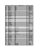
Page 38: ...rging ON OFF input terminal 19 S P I Serial parallel switching input terminal connected to power supply 20 DV DD I Power supply input terminal 21 CLK I DC DC converter external clock input terminal 22 PREGND GND terminal 23 AREF O Audio reference output terminal 24 AVCC O Ripple filter output terminal 25 CRP I Ripple filter smoothing capacitor connection terminal 26 RESET O Reset detection output ...

Page 39: ...r supply input terminal 38 SSW 39 SV CC 40 USW I DC DC converter coil drive input terminal 16 5 IC501 MN662782RPT1 Servo Processor Digital Signal Processor Digital Filter and D A Converter Pin No Mark I O Division Function 1 DV DD 5V Power supply terminal 5V 2 3 D0 D1 I O DRAM data input output terminal 4 NWE O DRAM write enable output terminal 5 NRAS O DRAM row address strobe output terminal 6 7 ...

Page 40: ...e adjustment output 30 TBAL O Tracking balance adjustment output 31 VREF I Reference voltage input 32 FE I Focus error input analog input 33 TE I Tracking error input analog input 34 RFENV I RF envelope signal input analog input 35 OFT I Off track signal input H Off track 36 NRFDET I RF envelope signal input L detect 37 BDO I Dropout signal input H dropout 38 LDON O Laser ON signal output H ON 39 ...

Page 41: ...d to GND 54 TMOD2 I Mode select signal input Connected to GND 55 FLAG O Not used open 56 FCLK IPFLAG O Phase synchronous signal output Interpolation flag terminal H interpolation 57 EXT0 ISRDATA I Serial data signal input 58 EXT1 ILRCK I L R discriminating signal input H Lch L Rch 59 EXT2 IBCLK I Serial bit clock 60 TX O Not used open 61 MCLK I Command clock signal input 62 MDATA I Command data si...

Page 42: ... 79 DV DD 1 Power supply digital circuit terminal 80 DV SS 1 GND digital circuit terminal 17 Replacement Parts List Notes Important safety notice Components identified by mark have special characteristics important for safety Furthermore special parts which have purposes of fire retardant resistors high quality sound capacitors low noise resistors etc are used When replacing any of components be s...

Page 43: ... 2 RFKKLVP48GKS CD COVER ASS Y 1 VP48 3 RGV0200 K1 SWITCH KNOB 3 4 RJC93020 1 BATTERY TERMINAL 1 5 RJF0032 JACK HOLDER 1 6 RKW0623 Q REMOTE CONT FILTER 1 7 XTN17 6GFZ SCREW 4 8 RME0308 OPEN SPRING 1 9 K0RE00400003 OPERATION P C B 1 10 RHE5119YA SCREW 4 11 RAE0145Z TRAVERSE DECK 1 11 1 RAF0142A OPTICAL PICKUP 1 11 2 RDG0305 GEAR 1 11 3 RDG0306 GEAR 1 11 4 RJB2106A TRAVERSE FPC 1 11 5 RMG0449 H FLOA...

Page 44: ...NUAL 1 A7 RFKFP3GAVT2S RECHARGEABLE BATT ASS Y 1 VP48 A7 1 RXQ0449 BATTERY CARRYING CASE 1 VP48 C10 ECUV1H121JCV 50V 120P 1 C11 ECUVNA105ZFV 10V 1U 1 F1H1A105A030 C12 ECST0JY475RR 6 3V 4 7U 1 ECST0JY475R C13 RCE0JSL470IX 6 3V 47U 1 F2D0J4700006 C14 RCEV0GA221G 4V 220U 1 C15 ECUZNC104ZFV 16V 0 1U 1 F1H1C1040008 C16 17 ECUVNA105ZFV 10V 1U 2 F1H1A105A030 C19 ECST0GY226RR 4V 22U 1 ECST0GY226R C20 ECUV...

Page 45: ...10V 1U 1 F1H1A105A030 C516 17 ECUVNH103KBV 50V 0 01U 2 F1H1H103A748 C525 ECUZNC104ZFV 16V 0 1U 1 F1H1C1040008 VP43 VP48 C526 ECST0JY475RR 6 3V 4 7U 1 ECST0JY475R VP43 VP48 C601 02 ECUV1H681KBV 50V 680P 2 C603 04 ECST0GY106RR 4V 10U 2 ECST0GY106R C607 08 ECUV1H221KBV 50V 220P 2 F1H1H2210001 C609 ECUVNA105ZFV 10V 1U 1 F1H1A105A030 C610 RCST0GY476RG 4V 47U 1 F3F0G4760001 C611 12 ECST1AY225RR 10V 2 2U...

Page 46: ...A030 C853 ECST0JY475RR 6 3V 4 7U 1 ECST0JY475R C854 ECUV1H102KBV 50V 1000P 1 C855 RCST0JC157RE 6 3V 150U 1 F3H0J157A001 C856 ECUVNA105ZFV 10V 1U 1 F1H1A105A030 C858 ECUVNA224KBV 10V 0 22U 1 F1H1A224A028 C859 60 ECUV1H470KCV 50V 47P 2 C871 ECUZNC104ZFV 16V 0 1U 1 F1H1C1040008 C872 ECST0JY475RR 6 3V 4 7U 1 ECST0JY475R C1000 01 ECUV1H100DCV 50V 10P 2 C1002 12 ECUZNC104ZFV 16V 0 1U 11 F1H1C1040008 C10...

Page 47: ...DBCAE00002 IC1000 MN89103M2 IC 1 IC1001 LH5V2RN0 IC 1 C3CBJC000012 IC1002 LC32V4260TLM IC 1 IC1003 TC7WU04FUT2L IC 1 IC1004 TC7W14FUTE1L IC 1 ICP11 RSFPB20ET L IC PROTECTOR 1 K5H102Z00002 ICP12 JAA2402631NA IC PROTECTOR 1 JK11 RJJ43K09 C DC IN 1 K2EB2B000006 JK601 RJJD3S5ZB C AUDIO OUT JACK 1 K2HC103B0061 JK701 RJJ33TK07 C H P JACK 1 K2HC103B0054 JK751 RJJD3S5ZB C MIC JACK 1 K2HC103B0061 VP48 JK80...

Page 48: ...NSISTOR 1 Q753 UN5117TX TRANSISTOR 1 UNR511700L VP48 Q754 55 XN1115TX TRANSISTOR 2 XN0111500L VP48 Q758 IMD16AT108 TRANSISTOR 1 B1GKCFEL0001 VP48 Q761 62 2SD1328QRSTX TRANSISTOR 2 VP48 Q803 FMG4T148 TRANSISTOR 1 B1GFCFJA0006 Q805 FMG4T148 TRANSISTOR 1 B1GFCFJA0006 Q851 XP161A1265PR TRANSISTOR 1 Q852 2SD1328QRSTX TRANSISTOR 1 Q855 2SD1328QRSTX TRANSISTOR 1 Q856 IMD16AT108 TRANSISTOR 1 B1GKCFEL0001 ...

Page 49: ...B473JA002 R501 ERJ3GEYJ683V 1 16W 68K 1 D0GB683JA002 R502 ERJ3GEYJ563V 1 16W 56K 1 R503 ERJ3GEYJ105V 1 16W 1M 1 R505 ERJ3GEYJ391V 1 16W 390 1 R506 ERJ3GEYJ222V 1 16W 2 2K 1 R508 ERJ3GEYJ100V 1 16W 10 1 R509 EXBV8V102JV 1 16W 1K 1 R513 ERJ3GEYJ104Z 1 16W 100K 1 R601 02 ERJ3GEYJ102V 1 16W 1K 2 ERJ3GEYJ102Z R603 04 ERJ3GEYJ473V 1 16W 47K 2 D0GB473JA002 R605 06 ERJ3GEYJ102V 1 16W 1K 2 ERJ3GEYJ102Z R60...

Page 50: ...J101V 1 16W 100 1 VP48 R782 ERJ3GEYJ473V 1 16W 47K 1 D0GB473JA002 VP48 R783 84 ERJ3GEYJ273V 1 16W 27K 2 D0GB273JA002 VP48 R785 ERJ3GEYJ102V 1 16W 1K 1 ERJ3GEYJ102Z VP48 R788 ERJ3GEYJ102V 1 16W 1K 1 ERJ3GEYJ102Z VP48 R801 ERJ3GEYJ223V 1 16W 22K 1 D0GB223JA002 R804 ERJ3GEYJ473V 1 16W 47K 1 D0GB473JA002 R806 EXBV8V102JV 1 16W 1K 1 R851 ERJ3GEYJ104Z 1 16W 100K 1 R852 ERJ3GEYJ153V 1 16W 15K 1 R853 ERJ3...

Page 51: ... 0 5 VP48 RJ516 ERJ3GEY0R00V 1 16W 0 1 VP43 RJ517 ERJ3GEY0R00V 1 16W 0 1 VP48 RJ601 RLBV102V Y COIL 1 J0JBC0000014 RJ602 ERJ3GEY0R00V 1 16W 0 1 RJ701 06 RLBV102V Y COIL 6 J0JBC0000014 RJ751 ECUZNC104ZFV 16V 0 1U 1 F1H1C1040008 VP33 VP43 RJ751 ERJ3GEY0R00V 1 16W 0 1 VP48 S201 ESE11SV6 SW LASER ON OFF 1 S202 ESE11HS4 SW REST DET 1 S309 RSS3A007 1A SW MODE 1 K0D113B00037 S310 RSS2A010 1A SW HOLD 1 K0...

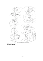
Page 52: ...19 Packaging 52 ...

Page 53: ...Printed in Japan H000900000 SW HH 53 ...
Page 54: ...PDA LD LPD RF RF IN CS BRT CEA C A D D B C LDON FO1 6 8 RO1 H BRIDGE PRE DRIVER LOGIC RI1 FO2 11 9 RO1 H BRIDGE PRE DRIVER LOGIC FI2 FO3 22 24 RO3 H BRIDGE PRE DRIVER LOGIC FO4 27 25 RO4 H BRIDGE PRE DRIVER LOGIC 5 TRAVERSE MOTOR SPINDLE MOTOR M M F F T T 29 30 AN8746SA E1 IC401 COIL MOTOR DRIVE 4 FI1 13 TR FO PDOWN TR FO SUBTRA CTOR 7 10 23 26 PGND1 PGND2 PGND3 PGND4 RI2 12 FI3 RI3 20 21 FI4 RI4 ...
Page 55: ...MES OVER SAMPLING DIGITAL FILTER SOFT MUTING DIGITAL ATTENUATION 1 BIT DAC PWM LOGIC OUTR OUTL 50 48 67 SRDATA DIGITAL AUDIO INTERFACE MNV4400DT8TL IC502 4M DRAM X501 16 9MHz 21 5 8 11 13 17 1 2 22 23 4 5 9 8 NCAS1 NCAS2 NRAS NWE NCAS NWE NRAS B2 12 VDD VSS 24 SERVO CPU SPPOL 22 SPOUT TR TR 25 TR TBAL FBAL 30 29 FO FBAL TBAL FO TRV LDON A0 9 DQ0 3 ADPVCC 41 60 TX PWM R L P F BCLK LRCK 65 66 SBCK 7...
Page 56: ...SEL 121 115 CDG SCK 122 CDG SDATA Vss 2 16 39 47 53 80 99 104 116 I O Vss 20 72 VGAIN 18 22 41 49 55 82 102 118 120 AV DD B2 66 70 74 87 AGND 68 71 76 85 B1 67 B1 61 VDDMAX IN VDDMAX OUT 109 V DD 3 B1 VMUTE 40 VMUTE 54 VCDRST 9 HRDY HINT 16 HSEL 12 10 HCK 6 CD C2PO 3 CD BCK 5 CD LRCK B1 Q803 805 DA EMP 34 DEMPH 119 HD IN 11 HDIO COMPOS OUT 73 VREF B2 77 78 CLK SEL 0 CLK SEL 1 B1 79 CLK SEL 2 81 CL...
Page 57: ...GITAL ECHO 6 5 SEL1 SEL2 B6 LCD301 L C D 29 N P NTSC PAL S314 NTSC PAL B8 22 WLSRCN B4 100 97 VL1 VL2 KEY SWITCH S302 304 308 311 313 1 KEY1 KEY2 KEY3 2 3 33 RESET 47 CHGCMP 46 STROBE 69 EMUTE E0 E1 M1 M0 70 EMUTE E0 68 E1 65 M1 66 M0 KPOWER 64 KPOWER RESET CHGCMP STROBE 28 MIC MIC 72 87 SEG1 16 92 95 COM0 3 Z351 REMOTE SENSOR Q11 12 RESET V cc B6 89 VREF B6 90 AVss GND 32 38 91 43 VPOWER 96 VL3 B...

Page 58: ...FT 2 DSW 22 PREGND 15 MSTAT ACDET AREF 33 OFF 32 SPRT 6 ICNT B4 VG START MCLK MLD MDATA CHGCMP RESET PMCK D21 RS10003E2 IC11 DC DC CONVERTER B5 14 REGB 4 VSEN 20 19 DVDD S P RIPPLE FILTER 23 24 25 CRP AVcc B3 D12 B4 AREF B7 U V LO VREF OSC L O S C P ER AMP PWM 3 2 1 4 5 6 7 8 L851 Q851 B3 Q852 855 B1 B2 VR851 VOLTAGE ADJ B9 C0DBCAE00002 IC851 DC DC CONV ICP12 Q10 B3 Q51 54 DC IN DET Q856 B3 MVcc G...

Page 59: ... 11 K VCD index button V INDEX L Microphone volume control button MIC Echo button ECHO M Program button PROGRAM N A B repeat button A B O Recall button RECALL P Time access button TIME ACCESS Q Clear button CLEAR R Select button 1SELECT S Pause button T Previous next buttons PREV NEXT 9 U Return button V Voice mode button MONO L R KARAOKE DUAL W Key control buttons fl SL VP48 SL VP48 SL VP48 SL VP...

Page 60: ...R511700L B1GDCFJN0011 B1GBCFJJ0007 E C B C B C E B C B C E MA2J11100L A Ca Anode Cathode MA2J70400L A Ca A Ca Anode Cathode Anode Anode Cathode Anode Cathode Anode Anode Cathode AN8746SA E1 AN8839NSB E1 LH5V2RN0 NJU7082BVAE1 RS10003E2 32PIN 28PIN 32PIN 8PIN 40PIN 8PIN 14PIN 16PIN 8PIN C0ABBB000105 C0ABBB000081 C1BB00000367 C0DBCAE00002 MNV7400CT10T 1 6 7 12 13 18 19 24 XP161A1265PR D G S 1 10 13 2...

Page 61: ...G H A B C E F I J K L M N D O P Q R S G H T U V W X A B C D E R121 120K R120 10K R122 120K C120 1500P C111 0 022 C113 0 1 A B C D E F G D E C B A H R114 33 IC401 AN8746SA E1 COIL MOTOR DRIVE A B D C 1 2 3 4 5 6 7 8 9 10 11 12 13 14 15 16 17 18 19 20 21 22 23 25 24 26 27 28 29 30 31 32 PV CC 1 V CC MON FI1 RI1 RO1 PGND1 FO1 FO2 PGND2 RO2 RI2 FI2 GND NC PV CC 2 PV CC 4 AC PC FI4 RI4 RO4 PGND4 FO4 FO...

Page 62: ... D301 M1MA141WKT1 W X U T S D E R C B A A B V Z351 RCDRS 52 REMOTE SENSOR R351 47K C351 6 3V4 7 C352 0 1 R352 220 RJ301 0 For SL VP48 ONLY R305 1K S310 HOLD S314 NTSC PAL S309 MODE R306 47K R307 47K R330 22K R331 22K For SL VP48 ONLY EXCEPT SL VP48 R328 22K P O N M L K J I H G U F E C D T S Q R C D E F G H I R304 1K M N C301 0 22 A B R303 1K F G H J K L O P Q SCHEMATIC DIAGRAM 2 V J Y A B A B R301...

Page 63: ...68K R513 100K C505 0 022 C506 0 22 R505 390 C509 0 01 R506 2 2K C508 0 47 C513 1 C507 4V220 R616 3 9K R615 3 9K R508 10 C607 220P C608 220P I Q X501 16 9MHz R503 1M C516 0 01 C510 0 1 C514 1000P S T J K L M N V U R O P M R S T U V W X Y Z SCHEMATIC DIAGRAM 3 MAIN CIRCUIT A J C517 0 01 RJ517 0 RJ511 0 RJ512 0 RJ513 0 RJ514 0 RJ501 0 RJ502 0 RJ503 0 RJ504 0 RJ505 0 RJ516 0 RJ515 0 N R509 1K RJ602 0 ...

Page 64: ...27K R852 15K C853 6 3V4 7 R854 12K C854 1000P C852 1 R851 100K C851 1000P S G D 1 2 3 4 5 6 7 8 IN F B GND OUT V CS CT REF C859 47P R860 10 D851 MA2J11100L Q852 C858 0 22 R861 22K C804 0 01 R858 15K VR851 3K B R857 82K D872 MA2J11100L D871 MAZ80510ML R872 10K R871 4 7K R873 15K C872 6 3V4 7 C871 0 1 D903 M1MA141WKT1 G W K T H C801 4V470 C803 15P R801 22K SCHEMATIC DIAGRAM 4 S C34 0 1 Q11 B1GDCFJN0...

Page 65: ...C22 0 1 C24 560P C20 1 C19 4V22 C12 6 3V4 7 C31 0 1 R34 68K L K D12 MA3J741E0L R14 2 2K R13 1K R R780 1K R779 680 R775 12K R774 6 8K C763 0 01 C768 4V47 C E D H G I C769 0 1 R766 39K C771 4V47 C772 0 1 C774 2200P R770 560 C758 1 R758 68K R760 47K C757 220P C762 1 C764 1000P R763 10K C761 1 R788 1K C767 0 22 C766 0 22 C765 0 1 R765 33 C754 1 R754 18K R755 82K C755 1 R778 120 R756 4 7K R757 10K C756...

Page 66: ...C611 10V2 2 R610 18K R609 18K R784 27K I Q JK11 DC IN 4 5V R783 27K R781 100 C775 1 C776 1 R782 47K ICP12 JAA2402631NA C15 0 1 CN11 ICP11 K5H3022A0001 C751 220P R751 47K C752 25V0 47 C620 0 1 O P F B JK751 MIC PLUG TYPE 3 5mm MONAURAL JK801 VIDEO OUT PLUG TYPE 3 5mm 2 R6 LR6 UM 3 BATTERIES 3V 2RECHARGEABLE BATTERYS 2 4V SCHEMATIC DIAGRAM 6 For SL VP48 ONLY For SL VP48 ONLY R752 12K RJ702 RJ703 RJ7...

Page 67: ...C NC NC NC NC MD14 MD13 MD12 MD11 MD10 MD9 MD8 MD7 MD6 MD5 MD4 MD3 MD2 MD1 MD0 CD BCK CD DATA CD LRCK CD C2PO VSS VSS VDD3 VDD3 I O VSS NC NC NC NC NC NC MA9 MA8 MA7 MA6 MA5 MA4 MA3 MA2 MA1 MA0 V DD MAX IN RESET RESERVED V DD 3 V SS V DD 3 V SS RAS1 RAS0 V DD 3 CAS V SS MWE MCE NC NC NC RESERVED RESERVED RESERVED RESERVED RESERVED RESERVED CLK SEL 3 CLK SEL 2 CLK SEL 1 CLK SEL 0 COMPOS OUT AGND AG...

Page 68: ... NC GND A16 A15 A12 A7 A6 A5 A4 A3 A2 A1 A0 D0 D1 D2 NC A17 A14 A13 A8 A9 A11 OE A10 CE D7 D6 D5 D4 D3 SCHEMATIC DIAGRAM 8 V SS NC V CC A3 A2 A1 A0 DQ1 DQ16 1 2 3 4 5 6 7 8 9 10 13 14 15 16 17 18 19 20 21 22 23 24 25 26 27 28 29 30 31 32 35 36 37 38 39 40 41 42 43 44 NC NC V CC DQ2 DQ3 DQ4 DQ5 DQ6 DQ7 DQ8 V CC WE RAS DQ15 DQ14 DQ13 V SS DQ12 DQ11 DQ10 DQ9 NC LCAS UCAS OE A8 A7 A6 A5 A4 V SS 1 8V 0...

Page 69: ...E C B Q702 E C B Q761 E C B Q753 C759 C752 C805 1 5 10 7 8 14 IC751 Q755 C C B E B Q754 C C B E B Q758 C BE E B C C771 C768 R771 R772 IC752 1 5 8 9 10 15 16 E C B Q762 1 2 3 4 5 6 8 10 11 9 12 13 15 17 19 21 23 25 27 29 14 16 18 20 22 24 26 28 30 CN801 C806 Q856 C B E E B C S D G Q851 C801 C855 D851 D21 VR851 3 2 1 L851 CN401 6 5 4 3 2 1 L11 L13 L12 S309 NOR PBG OFF RESUME OFF ON S310 SHORT LAND Q...

Page 70: ...04 C611 C612 C707 C615 C604 C603 C853 C19 C12 C27 C28 C13 C33 C872 1 4 5 8 IC701 1 4 5 8 IC601 IC851 Q608 C C B E B Q871 C C B E B E C B Q604 L871 L801 L802 D872 D871 E C B Q601 E C B Q852 E C B Q855 E C B Q602 E C B Q54 E C B Q12 E C B Q11 1 4 5 8 E C B Q51 D12 D11 D101 1 5 10 15 20 21 25 30 35 40 IC11 IC401 ICP12 E C B Q201 D903 1 5 10 15 16 17 20 25 30 32 R508 R502 IC101 IC301 1 5 10 15 14 20 2...

Page 71: ...R605 R606 R607 R608 R609 R610 R611 R612 R613 R614 R701 R702 R705 R706 R709 R710 R711 R712 R713 R714 R715 R716 R804 R851 R852 R853 R854 R855 R859 R860 R871 R872 R873 C10 C12 C13 C15 C16 C17 C19 C20 C21 C22 C24 C26 C27 C28 C33 C34 C103 C114 C115 C351 C514 C517 C601 C602 C603 C604 C611 C612 C615 C617 C618 C620 C701 C702 C703 C704 C707 C780 C803 C804 C851 C852 C853 C854 C859 C860 C871 C872 Ref No Lo N...

Page 72: ...06 R1010 C1019 C1021 X1000 TP18 TP19 TP30 GND 23 25 30 32 35 40 44 C1003 1 5 10 13 15 20 22 C1004 IC1002 To A MAIN P C B CN801 IC1000 IC1001 IC1002 IC1003 IC1004 L1000 L1002 X1001 CN1001 TP1 TP2 TP3 TP4 TP5 TP6 TP7 TP8 TP9 TP10 R1000 R1001 R1002 R1003 R1004 R1005 R1006 R1007 R1008 R1009 R1010 R1011 R1012 R1013 R1014 R1020 C1000 C1001 C1002 TP12 TP13 TP14 TP15 TP16 TP17 TP18 TP19 TP20 TP21 TP22 TP2...

Reviews: