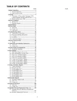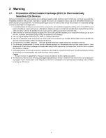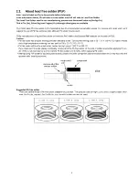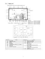
1 Safety Precautions
1.1.
General Guidelines
1. W hen servicing, observe the original lead dress. If a short circuit is found, replace all parts which have been overheated or
damaged by the short circuit.
2. A fter servicing, see to it that all the protective devices such as insulation barriers, insulation papers shields are properly
installed.
3. A fter servicing, make the following leakage current checks to prevent the custom er from being exposed to shock hazards.
4. W hen servicing, observe the original lead dress. If a short circuit is found, replace all parts which have been overheated or
damaged by the short circuit.
5. A fter servicing, see to it that all the protective devices such as insulation barriers, insulation papers shields are properly
installed.
6. A fter servicing, make the following leakage current checks to prevent the custom er from being exposed to shock hazards.
1.2.
Touch-Current Check
1. Plug the AC cord directly into the AC outlet. Do not use an isolation transform er for this check.
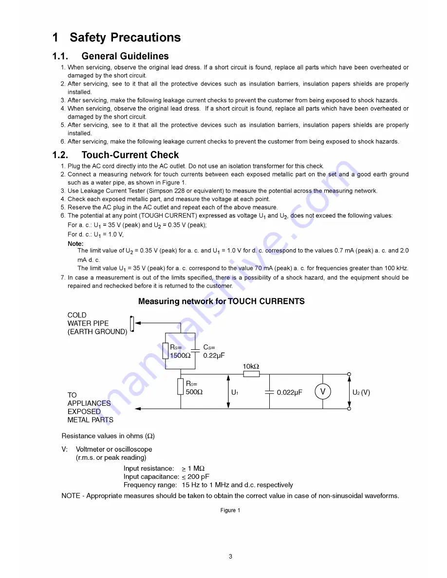
2. Connect a measuring network for touch currents between each exposed metallic part on the set and a good earth ground
such as a w ater pipe, as shown in Figure 1.
3. Use Leakage Current Tester (Simpson 228 or equivalent) to measure the potential across the measuring network.
4. Check each exposed metallic part, and measure the voltage at each point.
5. Reserve the AC plug in the AC outlet and repeat each of the above measure.
6. The potential at any point (TOUGH CURRENT) expressed as voltage U-| and U2, does not exceed the following values:
For a. c.: U-| = 35 V (peak) and U2 = 0.35 V (peak);
F o rd , c.: U-, = 1.0 V,
Note:
The limit value of U2 = 0.35 V (peak) for a. c. and U-| = 1.0 V for d. c. correspond to the values 0.7 mA (peak) a. c. and 2.0
mA d. c.
The limit value U-| = 35 V (peak) for a. c. correspond to the value 70 mA (peak) a. c. for frequencies
greater than 100 kHz.
7. In case a measurement is out of the limits specified, there is a possibility of a shock hazard, and the equipm ent should be
repaired and rechecked before it is returned to the customer.
Measuring network for TOUCH CURRENTS
METAL PARTS
Resistance values in ohms (Q)
V:
Voltmeter or oscilloscope
(r.m.s. or peak reading)
Input resistance:
> 1 MQ
Input capacitance: < 200 pF
Frequency range: 15 Hz to 1 MHz and d.c. respectively
NOTE - Appropriate measures should be taken to obtain the correct value in case of non-sinusoidal waveforms.
Figure 1
3
Summary of Contents for SP-R54Z1
Page 24: ...6 4 No Picture Drive circuits LED indicator f i i D16583 j D16253 SC Board SS Board 24 ...
Page 42: ...42 ...
Page 43: ...10 Block Diagram 10 1 Main Block Diagram Tuner box 43 ...
Page 45: ...10 3 Tuner box 1 3 Block Diagram и FR O N T TERM INAL 45 ...
Page 48: ...10 6 Display unit 1 4 Block Diagram d a d ig it a l s ig n a l p r o c e s s o r 48 ...
Page 50: ...10 8 Display unit 3 4 Block Diagram E POW ER SUPPLY 50 ...
Page 52: ...52 ...
Page 59: ...12 2 Tuner box 12 2 1 G and K Board Schematic Diagram с D E F 1 2 3 4 ...
Page 60: ...5 1 6 1 7 1 8 1 9 58 ...
Page 61: ...12 2 2 А В С D Е F GS Board Schematic Diagram 1 2 3 4 5 6 7 8 9 59 ...
Page 63: ...12 2 4 A Board 2 28 Schematic Diagram Д A BOARD 2 28 TXN A1JXUR TO DH BOARD DH72 10 11 12 13 ...
Page 64: ...т о K BOARD 14 15 16 17 18 61 ...
Page 68: ...еэ 9 se ре ее ге ...
Page 70: ...о 41 42 43 44 45 64 ...
Page 72: ...51 52 53 54 ...
Page 74: ...A D M PX NON USE Adress Data Multi PleX 59 60 61 66 ...
Page 77: ...SS NON USE SS PDP EEPROM EEPROM IC 8502 TVRQ771AA 16K BIT 2K BYTE 78 79 80 81 ...
Page 85: ...131 132 133 134 135 74 ...
Page 87: ...140 141 142 143 144 75 ...
Page 93: ... D D R 2 _ 0 IC5001 C3ABRY000038 185 186 187 188 189 80 ...
Page 96: ...203 204 205 206 207 82 ...
Page 98: ...12 2 27 A Board 25 28 Schematic Diagram 217 218 219 2 2 0 221 2 2 2 223 224 225 84 ...
Page 101: ...SUB3 3V г г 3 IC5300 т г т n I I COCSOBDOOOA gc o s j v I u т T 1 239 240 241 242 243 86 ...
Page 106: ...12 3 Display unit 12 3 1 P SUS Board Schematic Diagram 91 ...
Page 107: ...12 3 2 P MULTI Board 1 2 Schematic Diagram 92 ...
Page 110: ...то Р M U LT I B O A R D AKS02B VTL32 ...
Page 111: ...12 3 5 А В С D Е F PB Board Schematic Diagram 95 ...
Page 112: ...12 3 6 GL KA J S and SG Board Schematic Diagram A В D E KEY SWITCH 1 2 3 4 ...
Page 113: ... S BOARD TNPA4863 га 5W2500 чм ЕЁЭ Ь 1 1 Р в 8 1 Ч 13 ИJ а I f 5 6 7 8 9 96 ...
Page 114: ...12 3 7 А В С D Е F GH Board Schematic Diagram 1 2 3 4 5 6 7 8 9 97 ...
Page 115: ...12 3 8 А В С D Е F DA Board 1 18 Schematic Diagram А DA BOARD 1 18 TZTNP02JW U E IIC г т п 98 ...
Page 122: ...60 61 62 63 ...
Page 124: ...б о о о 00 О О О 68 69 70 71 72 105 ...
Page 125: ...12 3 16 DA Board 9 18 Schematic Diagram 73 74 75 76 77 78 79 80 81 106 ...
Page 126: ...12 3 17 DA Board 10 18 Schematic Diagram IC 25100 MN84527 I sc 82 83 84 85 ...
Page 127: ...86 87 88 89 90 107 ...
Page 129: ...12 3 19 DA Board 12 18 Schematic Diagram 100 101 102 103 104 105 106 107 108 109 ...
Page 130: ...12 3 20 DA Board 13 18 Schematic Diagram 109 110 111 112 113 114 115 116 117 110 ...
Page 131: ...12 3 21 DA Board 14 18 Schematic Diagram 118 119 120 121 122 123 124 125 126 111 ...
Page 136: ...J A 3 PB BOAftD PB6j 9 _ 3 v 9 _ _ Jrovie 9 1 9 ir low Z 5 TO Ы 9 159 160 161 162 ...
Page 137: ...12 3 26 C1 Board 1 2 Schematic Diagram C1 BOARD TNPA4770AC 1 2 В D F 1 2 ...
Page 138: ...мН I i h I I CB2 11 j l j i n I L i Г 116 ...
Page 141: ...12 3 29 C2 Board 2 2 Schematic Diagram 10 11 12 13 14 15 16 17 18 119 ...
Page 142: ...12 3 30 C3 Board 1 2 Schematic Diagram D E A СЗ BOARD TNPA4772AC 1 2 В F 1 9 120 ...
Page 143: ...12 3 31 C3 Board 2 2 Schematic Diagram A СЗ BOARD TNPA4772AC 2 2 10 11 12 13 ...
Page 144: ...14 15 16 17 18 121 ...
Page 150: ...12 3 37 SS Board 2 2 and SS2 Board Schematic Diagram 10 11 12 13 14 15 16 17 18 127 ...
Page 154: ...A BOARD COMPONENT SIDE TXN A1JXUR 130 ...
Page 166: ...P MULTI BOARD COMPONENT SIDE ETX2MM718EBS A I В I С I D I Ё 138 ...
Page 171: ...13 2 6 DA Board ...
Page 173: ...DA BOARD COMPONENT SIDE TZTNP02JWUE A I В I С I D I E I F I G I H I I 144 ...
Page 184: ...SS2 B0ARD COMPONENT SIDE TNPA4843 H 153 ...
Page 185: ...154 ...
Page 187: ...14 1 2 Exploded View 2 Display unit 1 156 ...
Page 188: ... 5 14 1 3 Exploded View 3 Display unit 2 157 ...
Page 189: ...14 1 4 Packing 1 158 ...
Page 190: ...14 1 5 Packing 2 TUNER BOX 159 ...
Page 191: ...14 1 6 Packing 3 160 ...
Page 192: ...14 1 7 Packing 4 Pedestal ...
Page 193: ...14 1 8 Packing 5 162 ...
Page 194: ...14 1 9 Packing 6 DISPLAY UNIT 163 ...
Page 195: ...14 1 10 Packing 7 164 ...


