background image

45

TC-P42GT30A

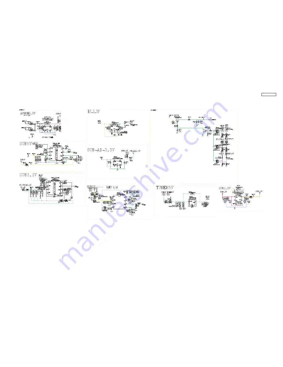
12.3. A Board Schematic Diagram - (1/20)

Summary of Contents for TC-P42GT30A

Page 1: ...ORDER No PBRAS1109097CE Model No TC P42GT30A GPF14D A Chassis Service Manual 2011 Panasonic do Brasil Limitada CS Division Technical Support Plasma Television ...

Page 2: ...Speakers 23 8 12 Remove the Stand bracket 24 8 13 Remove the K Board 24 8 14 Remove the S Board 24 8 15 Remove the V Board 24 8 16 Remove the Bottom cabinet assy 24 8 17 Remove the Plasma panel from the Cabinet assy 25 8 18 Remove the Contact metals 25 8 19 Remove the C1 Board 25 8 20 Remove the C2 Board 26 8 21 Replace the Plasma panel 26 9 Measurements and Adjustments 27 9 1 Adjustment 27 10 Blo...

Page 3: ...azards 1 2 Touch Current Check 1 Plug the AC cord directly into the AC outlet Do not use an isolation transformer for this check 2 Connect a measuring network for touch currents between each exposed metallic part on the set and a good earth ground such as a water pipe as shown in Figure 1 3 Use Leakage Current Tester Simpson 228 or equivalent to measure the potential across the measuring network 4...

Page 4: ...posure of the assembly 3 Use only a grounded tip soldering iron to solder or unsolder ES devices 4 Use only an anti static solder removal device Some solder removal devices not classified as anti static ESD protected can generate electrical charge sufficient to damage ES devices 5 Do not use freon propelled chemicals These can generate electrical charges sufficient to damage ES devices 6 Do not re...

Page 5: ...Pb free solder has a higher melting point than standard solder Typically the melting point is 50 70 F 30 40 C higher Please use a high temperature soldering iron and set it to 700 20 F 370 10 C Pb free solder will tend to splash when heated too high about 1100 F or 600 C If you must use Pb solder please completely remove all of the Pb free solder on the pins or solder area before applying Pb sol d...

Page 6: ...e Function Board Name Function P Power Supply C1 Data Driver Lower Right A Main AV input processing C2 Data Driver Lower Left K Remote receiver Power LED C A T S sensor SN Scan Drive S Power switch SS Sustain Drive V 3D Eyewear transmitter SS2 Sustain out Lower ...

Page 7: ...25 576 50i 625 576 50p 750 720 60p 750 720 50p 1 125 1 080 60i 1 125 1 080 50i 1 125 1 080 60p 1 125 1 080 50p 1 125 1 080 24p Signal name Horizontal frequency kHz Vertical frequency Hz 640 400 70 Hz 31 47 70 07 640 480 60 Hz 31 47 59 94 640 480 75 Hz 37 50 75 00 800 600 60 Hz 37 88 60 32 800 600 75 Hz 46 88 75 00 800 600 85 Hz 53 67 85 06 852 480 60 Hz 31 44 59 89 1 024 768 60 Hz 48 36 60 00 1 02...

Page 8: ...e RCA 1 1 0 V p p 75 Salida Audio AUDIO L R Tipo Pine RCA 2 0 5 V rms alta impedância Otros Entrada HDMI 1 4 Conectores Tipo A Es ta TV soporta la función HDAVI Control 5 Entrada PC D SUB de 15 Pines de alta densidad R G B 0 7 V p p 75 HD VD Nível TTL 2 0 5 0 V p p alta impedância DIGITAL AUDIO OUT PCM Dolby Digital DTS Fibra óptica Ranura para Tarjeta Ranura para Tarjeta 1 USB 1 2 3 Conectores US...

Page 9: ...me After the replacement of IC SELF CHECK should be done to generate the final KEY data How to SELF CHECK While pressing VOLUME button on the main unit press MENU button on the remote control for more than 3 seconds TV will be forced to the factory shipment setting after this SELF CHECK 5 1 3 Model and Keys 5 2 USB HDD Recording 5 2 1 General information Digital TV programmes can be recorded in US...

Page 10: ...Service Mode 6 1 2 Key command 1 button Main items Selection in forward direction 2 button Main items Selection in reverse direction 3 button Sub items Selection in forward direction 4 button Sub items Selection in reverse direction RED button All Sub items Selection in reverse direction GREEN button All Sub items Selection in forward direction VOL button Value of sub items change in forward direc...

Page 11: ...M STBY SET 00 EMERGENCY ON Y C Delay OPT 1 10110000 OPT 2 00100010 OPT 3 00000001 OPT 4 00010000 EDID CLK MID MIRROR 00 See Option Mirror AMR SELECT OFF VSUS HIGH See Vsus selection AGING ALL WHITE Built in test patterns can be displayed ALL BLUE WITH WHITE OUTSIDE FRAME ALL GREEN ALL RED LOW STEP WHITE LOW STEP BLUE LOW STEP GREEN LOW STEP RED WHITE DIAGONAL STRIPE RED DIAGONAL STRIPE GREEN DIAGO...

Page 12: ...istory SOS History Number of LED blinking indication From left side Last SOS before Last three occurrence before 2nd occurrence after shipment 1st occurrence after shipment This indication will be cleared by Self check indication and forced to factory shipment setting 6 3 3 POWER ON Time Count Note To display TIME COUNT menu highlight position then press MUTE for 3 sec Time Cumulative power on tim...

Page 13: ...amme number Selection Off 0 to 99 Off give priority to a last memory Initial VOL Level Adjust the volume when each time power is switched on Selection Range Off 0 to 100 Off give priority to a last memory Maximum VOL Level Adjust maximum volume Range 0 to 100 Button Lock Select local key conditions Selection Off SETUP MENU ALL Off altogether valid SETUP only F key is invalid Tuning guide menu can ...

Page 14: ...ther TVs 6 5 2 Preparation Make pwd file as startup file for a or b in a empty SD card 1 Insert a empty SD card to your PC 2 Right click a blank area in a SD card window point to New and then click text document A new file is created by default New Text Document txt 3 Right click the new text document that you just created and select rename and then change the name and extension of the file to the...

Page 15: ...t a following password for a or b by using remote control a For Board replacement 2770 b For Hotel 4850 Data will be copied from TV set to SD card It takes around 2 to 6 minutes maximum for copying 4 After the completion of copying to SD card remove SD card from TV set 5 Turn off the TV set Note Following new folder will be created in SD card for data from TV set a For Board replacement user_setup...

Page 16: ...lacement 2771 b For Hotel 4851 Data will be copied from SD card to TV set 4 After the completion of copying to SD card remove SD card from TV set a For Board replacement Data will be deleted after copying Limited one copy b For Hotel Data will not be deleted and can be used for other TVs 5 Turn off the TV set Note 1 Depending on the failure of boards function of Data copy for board replacement doe...

Page 17: ...iewed See Chap 5 Produce TV reception screen and while pressing VOLUME button on the main unit press MENU button on the remote con trol for more than 3 seconds 7 1 2 Screen display 7 1 3 Check Point Confirm the following parts if NG was displayed 7 1 4 Exit Disconnect the AC cord from wall outlet or switch off the power with Power button on the main unit DISPLAY Check Ref No Description Check P C ...

Page 18: ... lit then turns red blinking a few seconds later See 7 2 3 Only red is lit Blinking Times Contents Check point 1 Panel information SOS LP1 Start SOS 3 P 3 3V SOS A Board 4 Power SOS P Board 5 P 5V SOS A Board 6 Driver SOS1 SN Energy recovery circuit A SN FPC DET SN Board A SN FPC 7 Driver SOS2 SN Connector DET SN Scan and Logic IC SN Board 8 Driver SOS3 SS FPC DET SS Energy recovery circuit SS Boa...

Page 19: ...19 TC P42GT30A 7 4 No Picture ...

Page 20: ...20 TC P42GT30A 7 5 Local screen failure Plasma display may have local area failure on the screen Fig 1 is the possible defect P C B for each local area Fig 1 ...

Page 21: ... 3 Remove the P Board Caution To remove P C B wait 1 minute after power was off for dis charge from electrolysis capacitors 1 Unlock the cable clampers to free the cable 2 Disconnect the connectors P2 P6 P11 P34 and P35 3 Remove the screws 5 and remove the P Board 8 4 Remove the Terminal covers and the shield metals 1 Remove the claw 1 2 Remove the Side terminal cover 3 Remove the claw 1 4 Remove ...

Page 22: ... A40 5 Remove the screw 1 and remove the A Board 8 6 Remove the Side unit assy 1 Disconnect the connector C14 2 Remove the claws 2 and remove the Side unit assy 3 Remove the screw 1 4 Remove the Side unit mount metal 8 7 Remove the SN Board 1 Disconnect the flexible cables SN1 SN2 SN3 SN4 SN5 SN6 SN7 and SN8 connected to the SN Board 2 Disconnect the connector SN2 3 Disconnect the flexible cable S...

Page 23: ...d See section 8 8 3 Disconnect the flexible cable SS66 4 Remove the screws 2 and remove the SS2 Board 8 10 Remove the Fan 1 Unlock the cable clampers to free the cable 2 Remove the screws 2 3 Remove the Relay connector and remove the Fan 8 11 Remove the Speakers 1 Unlock the cable clampers to free the cable 2 Remove the screws 2 5 and remove the SP shield metal L 3 Remove the screws 2 5 and remove...

Page 24: ... 5 Disconnect the connector K1 and remove the K Board from the LED panel 8 14 Remove the S Board 1 Remove the SP shield metal L See section 8 11 2 Remove the screws 2 3 Disconnect the connector S10 and remove the S Board 8 15 Remove the V Board 1 Remove the SP shield metal R See section 8 11 2 Remove the Stand bracket See section 8 12 3 Remove the screw 1 and remove the claws 3 4 Disconnect the co...

Page 25: ... metals 1 Remove the Cabinet assy See section 8 17 2 Remove the Tape from the Contact metals 3 Remove the screws 6 4 Remove the Contact metal side L R 5 Remove the screws 6 6 Remove the Contact metal top 7 Remove the screws 15 8 Remove the Contact metal bottom 8 19 Remove the C1 Board 1 Remove the Contact metal bottom See section 8 18 2 Disconnect the flexible cables CB1 CB2 CB3 CB4 CB5 CB6 and CB...

Page 26: ...eplace the Plasma panel Caution Place the Plasma panel on a flat surface of a table cov ered by a soft cloth and a cushion A new Plasma panel itself without Contact metals is fragile To avoid the damage to new Plasma panel carry a new Plasma panel taking hold of the Contact metals 1 Place a carton box packed a new Plasma panel on the flat surface of the work bench 2 Open a box and without taking a...

Page 27: ...en Display will be displayed during TEST and CONF stage Press 5 button to display the On Screen Display 3 Press VOL button to set to LOW 4 In LOW setting a If no several dead pixel is visible remarkably in white pattern press 3 button to go to CONF stage b If the several dead pixels are visible remarkably in white pattern Set to HIGH by press VOL button Press 3 button to go to CONF stage if the sy...

Page 28: ...ide under automatic adjustment 3 The OSD character of sub contrast returns to black When NG is displayed adjustment failure 4 End Note Sub contrast adjustment is unadjusted for AV HD input But when needing the adjustment cho sen manually please refer to alterna tive method Steps Remarks Another procedure Connect IIC cable bus controller cable after banner OSD appear And after SRQ L begin an adjust...

Page 29: ...ll White or Split colour bar receive component signal as shown below 2 Goes into service mode 3 Push 1 or 2 key and goes into adjustment mode for CONTRAST Adjustment 1 The colour key yellow button of remote control is pushed 2 The OSD character of sub contrast becomes red Inside under automatic adjustment 3 The OSD character of sub contrast returns to black When NG is displayed adjustment failure ...

Page 30: ...Steps Remarks copy adjustment Connect IIC cable bus controller cable after banner OSD appear And after SRQ L begin an adjustment 2 seconds later Make sure the front panel to be used on the final set is fitted Make sure a color signal is not being shown before adjustment Put the color analyzer where there is little color variation Note Copy Adjustment method in service mode When you push OK key in ...

Page 31: ...DRIVE set to FF 9 Set color balance to NORMAL using 7 key 10 Fix G CUTOFF B CUTOFF and R CUTOFF at 80 11 Set G DRIVE at D0 12 Adjust B DRIVE and R DRIVE so the INNER PATTERN x y become the COLOR TEMP NORMAL in the table 1 13 All RGB drive increase so that the maximum drive value of RGB may become FF ALL DRIVE set to FF 14 Set color balance to WARM using 7 key 15 Set Picture menu to CINEMA using 9 ...

Page 32: ...number key 0 is operated and select METHOD 03 4 A number key 5 is operated and INNER PATTERN is displayed INNER PATTERN 5 Select G CUTOFF item using the number key 3 or 4 and set to 80 using the volume key or Also B CUTOFF and R CUTOFF set to 80 6 Set G DRIVE at D0 7 Touch the signal receiver of color analyzer to the highlight window center and adjust B drive and R drive so x y become the COLOR TE...

Page 33: ...33 TC P42GT30A ...

Page 34: ...34 TC P42GT30A ...

Page 35: ... EEPROM NAND FLASH TUNER AMP CVBS Y PR C PB HDMI I F STB3 3V KEY1 SUB3 3V C A T S SENSOR SUB3 3V PWM L R L R Y PB PR PC L R R G B AV1 V AV2 AV3 L R V A OUT L R AUDIO OUT HP OUT HEADPHONE L R SUB3 3V SUB3 3V DCDC G LED LED G AUDIO OUTPUT L R VIDEO DATA MAIN SW2 VDA VSUS POWER SW SOUND15V DATA DRIVER P 15V ENERGY RECOVERY SUSTAIN P 3 3V P 5V SS VDA DATA DRIVER SS2 DATA DRIVER RELAY POWER FACTOR CONT...

Page 36: ..._ON SDVOLC DDC_IIC1 IC8706 9V MAIN_FAN_ON SW_OFF_DET VCC Y IC8000 SDVOLC USB2 TUNER_SUB_ON POWER_DET FAN_SOS SD CARD IC3753 IC8902 MAIN_FAN_ON CVBS YPbPr RGB YC TU4801 2 P6 SOS4_PS FAN_SOS 13 SOS4_PS C A T S_SENSOR SUB1 2V REMOTE IN FAN_MAX L R LVDS DATA XRST L R FAN_MAX PDP_DRVRST HDMI_5V_DET1 DDR3 I F 5 5V SPEAKER_L 7 IC8531 JK3007 XRST A STM LP1_XRST_SYS PANEL_SOS JK4602 NAND FLASH SUB1 8V DRVR...

Page 37: ... 3D EYEWEAR D_UHZ 20 A 55 P 5V 2 DRVRST_ IN 9 LED3 19 SOS6_SC1 LP1_XRST_SYS SOS8_SS SPI FLASH 14 DCDCEN SS33 SCAN CONTROL P 5V IC5901 SUSTAIN CONTROL TRANSMITTER STB 3 3V P_S0 LED1 PWM 29 9 LEDDRV5V 12 STB 1 2V IR LED DRIVER STB5V_SW_ON POWER_DET SOS_DCC IR_LR LED2 KEY1 A32 2 FLASH I F UHZ LED1 LED2 LED3 1 IIC0 IIC3 DMD_IIC0 VIDEO DATA 18 IC5900 1 IC9304 SOS7_SC2 5V DISCHARGE CONTROL A20 3 FAULT 4...

Page 38: ...06 T200 AC DET STB CONTROL IC200 PHOTO COUPLER PC201 L100 D505 IC400 10 13 STB5V_ON 5 SOS_P4 4 STB5V S0 S1 PANEL_MAIN_ON SOS_P4 D601 F_STBY ERROR DET D202 L100 Q102 03 Q100 01 FET DRIVER CONTROL GD2 IC300 VCC RESONANCE CONTROL OC SS L300 GD1 T300 RT D600 D700 VR600 IC600 Vda Vda ERROR DET Q600 PHOTO COUPLER PC700 PC400 PHOTO COUPLER PC401 PHOTO COUPLER VR251 IC700 Vsus Vsus ERROR DET Vsus Adj Q404...

Page 39: ...16561 62 SCAN CONTROL INVERTER CML P 15V Q16607 CSH IC14601 03 PDP SCAN OC1 PLASMA PANEL PANEL SCAN ELECTRODE LED G P2 VHIZ GEN SOS7 Q16402 Vsus VOL IC16563 Q16441 CLK OC1 SEL OC2 CSL IC14804 06 IC16784 85 IC16691 IPD CIRCUIT OC2 NAND IC16792 93 1 SN 20 SN21 SN22 SN23 SN24 SN25 SN26 SN27 SN28 D16713 T16472 VFG Q16601 CPH1 IC16684 BUFFER CMH SUSTAIN H BUFFER IC16501 IC16502 CSH BUFFER RECOVERY H CS...

Page 40: ...ction Diagram 11 1 Caution statement Caution Please confirm that all flexible cables are assembled correctly Also make sure that they are locked in the connectors Verify by giving the flexible cables a very slight pull 11 2 Wiring 1 ...

Page 41: ...41 TC P42GT30A 11 3 Wiring 2 11 4 Wiring 3 ...

Page 42: ...42 TC P42GT30A 11 5 Wiring 4 11 6 Wiring 5 ...

Page 43: ...43 TC P42GT30A Model No TH P42GT30A Schematic Diagram Note 12 Schematic Diagram 12 1 Schematic Diagram Note ...

Page 44: ...2 3 6 5 4 F100 K5E802YY0002 Y F101 K5E802YY0002 F102 K5E402YY0004 Y C1 C1 G G ZA100 K4ZZ01000206 ZA600 K4ZZ01000206 PC402 B3PAA0000363 PC700 B3PAA0000363 PC201 B3PAA0000363 PC400 B3PAA0000363 PC401 B3PAA0000363 PC200 B3PAA0000363 F501 K5H1022A0031 N TP301 TP302 TP505 TP506 TP507 TP508 TP700 TP701 TP702 TP703 TP006 TP704 TP504 TP003 TP502 TP501 TP500 TP202 TP203 TP104 TP601 TP602 TP603 TP707 TP204 ...

Page 45: ...45 TC P42GT30A 12 3 A Board Schematic Diagram 1 20 ...

Page 46: ...0066 1 5A D5704 B0ACCJ000048 D5622 B0ACCJ000048 D5621 B0ACCJ000048 D5624 B0BC010A0007 D5626 DZ2J033M0L IC5607 C0DBAYY00931 LV5876MXL TLM H 2 0A 1 BOOT 2 VIN 3 SW 4 GND 5 FB 6 COMP 7 8 SS Thermal_Pad A8 BM12B GVHS TB LF SN K1KY12AA0719 1 2 3 4 5 6 7 8 9 10 11 12 L5609 G1C6R8MA0445 C C C C C C C SUB5V P15V VJ5658 TP5614 TP5612 TP5617 TP5600 TP5618 TP5616 TP5615 TP5613 P_XIRQ5 P_PORT03 P_PORT02 R5705...

Page 47: ... P_PWM0LP PWM_WO_L P_LIN1_RP GUARD_SR P_LIN1_LP GUARD_SL GUARD_SL GUARD_SR GUARD_SL NET00753 NET00754 GUARD_SR PWM_WO_R PWM_WO_R AMP_STBY P_NSHUTDOWN C4941 10u 10V C4942 10u 10V C4925 25V 1u C4915 25V 1u C4921 25V 1u C4912 10u 25V C4922 10u 25V C4911 25V 1u C4931 16V 0 1u C4930 16V 0 1u C4929 25V 0 47u C4919 25V 0 47u C4928 25V 0 47u C4918 25V 0 47u C4916 0 1u 50V C4914 0 1u 50V C4924 0 1u 50V C49...

Page 48: ...C PC_HS MAIN_Y CVBS MAIN_L MAIN_PR P_LO1_L MAIN_PR PC_VS AC_TV1_V MAIN_Y CVBS BE_SCL3 MAIN_L BE_SCL3 BE_SDA3 AC_TV1_V D1_PR D1_PB D1_Y PC_H PC_V V1_VG MON_RG V1_LG V1_RG MAIN_R D1_PRG D1_YG D1_PBG PC_R PC_H PC_V PC_GG MON_VG GUARD_CLK SPDIF_OUT GUARD_CLK D1_PR D1_PB D1_Y PC_RG PC_BG PC_G PC_B V1_V V2_VG MON_LG V1_L V1_R D1_RG D1_LG D1_L D1_R V2_RG V2_LG PC_R PC_RG PC_G PC_GG PC_B PC_BG V1_L V1_R V...

Page 49: ...2 P_STM5VDET2 P_STMDCDCSDA3 sheet704 LOCK_PEAKS_DEST PU C PU C OD TESTSEL Don t care to floating when power on 5mA 4mA P_XTALSEL0 sheet011 CONECTOR PU C P_STMADIN0 P05 B5 R_LED_ON P_STMHPD0 SD_REC_READY HSP_SBI PD P_STMHPD1 P42 5mA 4mA P41 PD P_STMGPIO7 HOTEL_SBI P40 PU C P30 CLK P_STMDCDCSDA2 P_STMTIME3 PU C OD B5 OD sheet013 OD P61 B5 P_STMSBO0 OD PA0 PU C P91 Drive Current 5mA 4mA Other PP 2mA ...

Page 50: ... POWER_DET 16 STB5V_SW_ON 17 BUFF_5V_IN 18 BUFF_3 3V_OUT 19 GND 20 BUFF_EN 21 SP_MUTE 22 A_MUTE 23 AUDIO_MUTE_IN 24 MONITOR_MUTE 25 MUTE_VCC 26 CD 27 STBRST 28 STB1 2V 29 STB3 3V 30 STB5V 31 SUB5V 32 SD_VCC C C C C C C C C C C C C C C C C C C C C C SUB3 3V VDDSD18V33V STB5V SUB9V STB3 3V F15V STB5V SUB3 3V P3 3V SUB5V STB1 2V STB3 3V VJ5000 R5603 VJ5001 VJ1012 VJ5016 VJ5017 TP5006 TP5005 TP5003 TP...

Page 51: ...0JYC0000068 L4508 J0JHC0000117 L4504 J0JHC0000117 L4506 J0JYC0000068 L4509 J0JYC0000068 L4511 J0JYC0000068 L4503 J0JYC0000068 L4500 J0JHC0000117 L4515 J0JYC0000068 L4507 J0JYC0000068 L4501 J0JYC0000068 L4512 J0JYC0000068 L4514 J0JHC0000117 L4502 J0JYC0000068 L4510 J0JYC0000068 C C C C C C C C C C C C C C C C C C C C C SUB3 3V HDMI_SW3 3V VJ4821 VJ4819 VJ4820 VJ4604 VJ4606 VJ4608 VJ4822 VJ4601 VJ46...

Page 52: ...NC 9 NC 10 NC 11 GND 12 P2 IRQ 13 P1 IRQ 14 P3 IRQ 15 NC 16 NC 17 NC 18 NC 19 NC 20 NC JK8533 K1FY104B0065 1 2 3 4 JK8531 K1FY104B0065 1 2 3 4 JK8532 K1FY104B0065 1 2 3 4 L8533 J0JHC0000045 L4801 J0JGC0000020 L4810 J0JCC0000278 L8532 J0JHC0000045 L4802 J0JGC0000020 L8531 J0JHC0000045 L4804 G1CR39J00009 L4803 G1CR39J00009 C C C C C C C C C C C C C C C C C C C C C C C C C C C C C C C C C C C C C C C...

Page 53: ...CLK2N P_TB1N P_S1 P_TF1P AA_STMSCL BE_SDA1 P_TA2N P_TC2P P_TD1P P_STMSCL P_TE2P P_TE2N BE_SCL1 P_STMTIME2 P_SCL3 P_STMADIN0 P_SCL0 TER_TUNER_SCL P_SBI0 AA_STMSDA BE_SDA0 P_TB2N P_DMDSCL1 P_DMDSCL0 P_TCLK1N P_TB2P P_DMDSDA0 BE_SCL3 P_TD2N P_STMSDA P_SDA0 AR_STB_SDA02 P_PORT07 P_TCLK1P P_SDA1 P_TC1N P_TB1P P_SBO0 P_STMTIME0 P_TCLK2P P_STMGPIO3 P_TF2P Q8900 DSA200100L R8961 EXB28V332JX JS1053 JS1050 ...

Page 54: ...6 IC9300 R5 PG8 IC9300 E20 PG3 IC9300 B6 EXTFLSI IC9300 P27 PG3 IC9300 AJ27 LVDOD15N IC9300 AK12 LVDOD31P IC9300 V26 miniLVDS_MON0 IC9300 L25 PG3 IC9300 G30 DCCOP22 IC9300 K6 PG2 IC9300 AC25 PG2 IC9300 J3 DCCOP1 IC9300 R30 PG1 IC9300 AG11 PG6 IC9300 E10 LRX_TXP_1 IC9300 E5 PG1 IC9300 AF25 DRAM_TEST23 IC9300 AE10 PG2 IC9300 N5 PG1 IC9300 U25 PG7 IC9300 N2 DCCOP28 IC9300 AG20 PG6 IC9300 D7 TC2 IC930...

Page 55: ...GND2 C C C AGND2 LEDDRV_5V F15V P3 3V P2 5V LEDDRV_5V F15V P1 1V P3 3V SUB5V P5V LEDDRV_5V VJ5906 VJ5907 VJ5905 VJ5908 R9869 VJ5909 VJ9803 VJ9801 VJ5901 R9868 VJ9805 VJ9820 VJ5902 PA5900 K5H1022A0031 TP9276 TP9268 TP9204 TP9202 TP9266 TP9203 TP5900 TP5911 TP5912 TP5910 TP5913 TP9274 TP9201 TP9283 TP9269 TP9277 TP9282 TP9280 TP9267 TP9281 TP9275 TD5900 P_PORT33 VESA IR_LR P_XIRQ10 DCDCEN Q9860 B1MB...

Page 56: ...8902 16V 0 1u C8903 16V 0 1u C8900 16V 0 1u C8901 16V 0 1u C3EBHY000009 IC8902 1 A0 2 A1 3 A2 4 GND 5 SDA 6 SCL 7 WP 8 Vcc C3EBGY000023 IC8901 BR24S16FJ WE2 1 A0 2 A1 3 A2 4 GND 5 SDA 6 SCL 7 WP 8 Vcc C3FBUY000008 IC8900 HY27UF082G2B TPIB 1 NC 2 NC 3 NC 4 NC 5 NC 6 NC 7 R B 8 RE 9 CE 10 NC 11 NC 12 VCC 13 VSS 14 NC 15 NC 16 CLE 17 ALE 18 WE 19 WP 20 NC 21 NC 22 NC 23 NC 24 NC 25 NC 26 NC 27 NC 28 ...

Page 57: ...h 8bit retry block 8 0011 Inner ROM boot address 5 1bit ECC 0010 Inner ROM boot address 5 4bit ECC 0001 Inner ROM boot address 4 1bit ECC 0000 Inner ROM boot address 4 4bit ECC PEAKS SLD2 CHVAL0 Premium IPPLL Freqency change 0 800MHz 1 600MHz Inner PD Resistance mode_sel_soft rev0_init CHDATA0 VCXO Select 0 Inner Internal PU Resestance reverse XTALSEL1 XTALSEL0 EA PullUP 0 NONUSE reverse Addr Data...

Page 58: ...CM2520 102 2P T002 1 1 2 2 3 4 T8301 G5BYC0000015 1 2 3 4 5 6 9 10 11 12 8 7 C C C C C C C C C C SUB3 3V SUB3 3V VJ8627 L8602 VJUMP1608 P L8606 VJUMP1608 P L8601 VJUMP1608 P TP8603 P_PHYRSTL P_MII_TXD1 P_MII_TXD3 P_MDC P_MII_TXEN P_MII_TXD2 P_MII_TXD0 P_MII_RXDV P_MII_RXCLK P_MII_COL P_MII_RXD0 P_MII_RXD1 P_MII_RXD2 P_MII_RXER P_MII_TXCLK P_MII_CRS P_MII_RXD3 P_MDIO_INTL P_MDIO R8654 EXB28V560JX 1...

Page 59: ...0A8 IC8000 B23 XEWE1 IC8000 C5 MM0DM0 IC8000 A27 XNFWE IC8000 AH15 PWM1LN IC8000 L7 MM1VREF0 IC8000 G18 MM0BA0 IC8000 M28 AVSSAPUSB IC8000 V17 AVDDPLL33 IC8000 AD13 LIN1_RP IC8000 E15 VDDIO15 IC8000 V6 MDC IC8000 J29 SDCD IC8000 AB4 LVVSS IC8000 R26 HS0BCLKIN IC8000 AK9 BSIQ_I IC8000 AH22 STMTIME4 IC8000 AD4 LVVSS IC8000 U7 TCON7 IC8000 B15 MM0DQ28 IC8000 AE25 STMDDCSDA1 IC8000 V11 LVVDD33 IC8000 ...

Page 60: ... C C C C C C C C C C C AVSSEVE C C C C C C C C C C C C C C SUB1 5V STB3 3V SUB1 2V HDMI3 3V VDDSD18V33V SUB1 8V SUB3 3V STB1 2V R8006 VJUMP1608 P R8003 VJUMP1608 P R8005 VJUMP1005 P R8004 VJUMP1005 P R8002 VJUMP1608 P R8007 VJUMP1005 P R8009 VJUMP1608 P TCON2 5V P_VDD33 P_AVDDSIF18 P_VDDSTM33 P_VDDA12 P_AVDDADA33 SUB1 2V P_VDD18 P_VDDIO15 P_VDDTCON25_33 P_AVDD33 P_VDD33 P_VDDR12 P_AVDDSATA P_VDDST...

Page 61: ...15 PGND2 16 TRIP2 17 SS2 18 V5FILT 19 VREG5 20 VIN 21 TRIP1 22 PGND1 23 DRVL1 24 SW1 L8100 G1C4R7MA0416 L8102 G1C3R3MA0460 PGND1 PGND1 AGND1 PGND1 PGND1 AGND1 PGND1 PGND1 PGND1 AGND1 PGND1 AGND1 DCDCIN SUB1 5V SUB1 2V R8116 R8112 TP8101 TP8100 DCDCEN Q8101 B1CFRD000077 RQ1E075VNTR Q8100 B1CFRD000077 RQ1E075VNTR Q8102 B1MBEDA00027 ECH8666 P TL H S1 G1 S2 G2 D2 D2 D1 D1 R8100 1 27k 0 5 R8106 2k 0 5 ...

Page 62: ... A10 VSS IC8200 P11 DQS2 IC8200 U1 VDDQ IC8200 P3 DQS3 IC8200 H1 VREFDQ IC8200 B12 VSSQ IC8200 H10 BA2 IC8200 U11 VDD IC8200 G12 VSS IC8200 J3 CS1 IC8200 D2 DQS0 IC8200 J11 CK IC8200 M11 DQ16 IC8200 C1 VDDQ IC8200 D11 DQS1 IC8200 K9 A4 IC8200 E4 VDDQ IC8200 L9 A7 IC8200 E12 VDDQ IC8200 A3 VSS IC8200 R12 VDDQ IC8200 F1 VDD IC8200 K12 VDD IC8200 R3 DQ29 IC8200 F10 DQ13 IC8200 A9 RESET IC8200 T11 DQ2...

Page 63: ...VC1_N P_AXO R8301 470 R8302 36 R8303 36 X8300 H0J245500110 7V24580002 LOCK LDA3 24 576MHz CLK AVSSSIF SIF ADC REF DMD VIDEO INPUT AVSSV AVSSV V ADC REF AVSSV TEST TEST USB SATA CLK move peaks_other sheet P_TESTSEL P_VDD33 R8310 27k GUARD_V GUARD GUARD GUARD C8310 1u 10V C8311 1u 10V C AVSSEVE C C P_USB0RREF P_VCOMP P_USB1RREF P_USB2RREF P_VREF1V5 P_AVDD33 1 R8304 6 2k 1 R8305 6 2k 1 R8307 6 2k A A...

Page 64: ...45 VDD33_0 46 DBGBUS16 47 DBGBUS15 48 TESTIO17 49 TESTIO18 50 TESTIO19 51 VDD33_1 52 VDD12_2 55 NC 56 NC 57 VDD12_1 58 NC 59 VDD33_2 60 VDD33_5 61 DBGBUS12 62 DBGBUS11 63 VDD33_6 64 DBGBUS10 65 VDD33_7 66 PWM1 67 VDD33_8 68 VDD12_0 69 RESETN 70 DBGSEL GND Exposed_Pad 17 VDD_DIV 18 REFCLKI0 35 TESTIO12 36 TESTIO11 53 DBGBUS14 54 DBGBUS13 71 TEST0 72 TEST1 L6850 J0JHC0000045 C C C C C C C C C C C C ...

Page 65: ... 5 6 7 8 C1 C1 C1 C1 C1 C1 C1 C1 C1 C1 SN2810 B3JB00000078 1 IOUT 4 NC 2 GND 3 VCC 5 GC1 6 GC2 TP2804 TP2812 TP2808 TP2806 TP2811 TP2802 TP2801 TP2805 TP2803 RM2810 B3RAD0000168 1 2 3 Q2810 B1ABCE000015 Q2812 B1ABCE000015 Q2811 B1ABCE000015 R2818 47k 1 R2816 1 62k R2813 22k R2811 100k R2814 10k R2810 47 R2817 22k R2812 220k R2815 47k 1 R2819 4 3k STB3 3V AI_SENSOR REMOCON GND STB3 3V R_LED_ON REMO...

Page 66: ...66 TC P42GT30A 12 24 S Board Schematic Diagram PUSH S10B 1 2 3 S10 1 2 3 SW2890 K0F126A00003 1 2 3 4 5 6 To P 5V STB_PS ...

Page 67: ...67 TC P42GT30A 12 25 SS Board Schematic Diagram ...

Page 68: ...ic Diagram TERM SIDE C16361 1000p 630V C16362 5600p 630V D16362 SS66 503725 1391 K1MY13BA0443 1 2 3 4 5 6 7 8 9 10 11 12 13 C2 C3 ZA16111 K4AA04D00002 ZA16011 K4AZ01D00004 ZA16116 K4AA04D00002 ZA16112 K4AA04D00002 ZA16012 K4AZ01D00004 TP56 ...

Page 69: ...EL1 4 SEL2 5 VCC2 6 VTH1 7 VTH2 8 VTH3 9 RAMP1 10 RAMP2 11 GND 12 VB 13 VCNT 14 CNT1 15 CNT2 16 CNT3 17 CIGBT 18 OUT 19 N C 20 COMP4 21 COMP3 22 COMP2 23 CEN 24 VCC1 IC16784 MIP3910MSSCF 1 VDD 2 NC 3 FB 4 LS 5 DRAIN 7 SOURCE 8 SOURCE IC16786 MIP3910MSSCF 1 VDD 2 NC 3 FB 4 LS 5 DRAIN 7 SOURCE 8 SOURCE IC16724 C0CBADE00049 BA178M05FP E2 OUT 3 2 COMMON IN 1 C0CBALC00012 IC16795 TA78L15F TE12L F Vin 3...

Page 70: ... 62 OUT51 63 OUT52 64 OUT53 65 OUT54 66 OUT55 67 OUT56 68 OUT57 69 OUT58 70 OUT59 71 OUT60 72 OUT61 73 OUT62 74 OUT63 75 OUT64 76 OUT65 77 OUT66 78 OUT67 79 OUT68 80 OUT69 81 OUT70 82 OUT71 83 OUT72 84 OUT73 85 OUT74 86 OUT75 87 OUT76 88 OUT77 89 OUT78 90 OUT79 91 OUT80 92 OUT81 93 OUT82 94 OUT83 95 OUT84 96 OUT85 97 OUT86 98 OUT87 99 OUT88 100 OUT89 101 OUT90 102 NC 103 NC 104 NC 105 VDDH 106 NC ...

Page 71: ...0V C2852 0 047u 10V C2850 0 047u 10V D2853 B3EB00000056 D2851 B3EB00000056 D2850 B3EB00000056 D2852 B3EB00000056 V14 K1KA06B00220 1 2 3 4 5 6 C C C C C C TP2850 TP2851 TP2852 TP2853 TP2854 GND LED1 LED2 LED3 LED4 GND 12 29 V Board Schematic Diagram ...

Page 72: ... D0GZ1R0JA020 1 2W R17132 1 D0GZ1R0JA020 R17117 1k D0GF102JA047 R17118 100 1 2W R17111 1 D0GZ1R0JA020 R17141 680 1 2W R17112 1 D0GZ1R0JA020 1 R17151 49 9 1 R17104 49 9 1 R17153 49 9 1 R17106 49 9 1 R17108 49 9 1 R17105 49 9 1 R17154 49 9 1 R17152 49 9 1 R17149 49 9 1 R17150 49 9 1 R17102 49 9 1 R17147 49 9 1 R17107 49 9 1 R17101 49 9 1 R17148 49 9 1 R17103 49 9 R17145 0 R17146 0 R17196 1k R17144 1...

Page 73: ...0 R17245 680 R17233 680 R17218 100 R17204 100 1 2W R17229 1 D0GZ1R0JA020 1 2W R17227 1 D0GZ1R0JA020 1 2W R17221 1 D0GZ1R0JA020 1 2W R17223 1 D0GZ1R0JA020 1 2W R17225 1 D0GZ1R0JA020 R17214 100 1 R17251 49 9 1 R17210 49 9 1 R17209 49 9 1 R17252 49 9 1 R17250 49 9 1 R17249 49 9 1 R17219 49 9 1 R17216 49 9 1 R17254 49 9 1 R17212 49 9 1 R17211 49 9 1 R17220 49 9 1 R17255 49 9 1 R17256 49 9 1 R17253 49 ...

Page 74: ...74 TC P42GT30A 13 Printed Circuit Boards 13 1 P Board Foil side ...

Page 75: ...75 TC P42GT30A 13 2 P Board Component side ...

Page 76: ...76 TC P42GT30A 13 3 A Board Foil side ...

Page 77: ...77 TC P42GT30A 13 4 A Board Component side ...

Page 78: ...78 TC P42GT30A 13 5 K S and V Boards ...

Page 79: ...79 TC P42GT30A 13 6 C1 Board 13 7 C2 Board ...

Page 80: ...80 TC P42GT30A 13 8 SN Board Foil side ...

Page 81: ...81 TC P42GT30A 13 9 SN Board Component side ...

Page 82: ...82 TC P42GT30A 13 10 SS Board Foil side ...

Page 83: ...83 TC P42GT30A 13 11 SS Board Component side ...

Page 84: ...84 TC P42GT30A 13 12 SS2 Board ...

Page 85: ...85 TC P42GT30A 14 Exploded View and Replacement Parts List 14 1 Replacement Parts List Note Model No TH P42GT30A Replacement Parts List Note ...

Page 86: ...GT30A 14 2 Exploded View and Mechanical Replacement Parts List 14 2 1 Cabinet Exploded View K Board V Board S Board 22 47 48 51 46 Assembly screws Stand pole 1 Pole cover 1 Stand Base 1 Solver 4 Black 4 Black 4 ...

Page 87: ...87 TC P42GT30A 14 2 2 Packing and Accessories Exploded View Stand mounting kit Positionig hole 3 ...

Page 88: ...2 FAN SPONGE 20 TMMJ117 RUBBER CUSHION 21 TMZ2AX5012 STAND BRACKET 23 TTU2B42GT30B CS REAR COVER 24 TXFKY5Z0028 BOTTOM CABINET ASSY 33 K2KYYYY00136 AV CABLE 34 K1HY20YY0007 PC CABLE 35 K2KYYYY00138 AUDIO CABLE 39 K7CXGYC00002 OPTICAL CABLE 40 TNQ2B5305 REMOTE CONTROL 41 K1TYYYY00158 TUNER CABLE 42 TPC2B42420 CARTON BOX 43 TPD2AA0304 PEDESTAL CUSHION 44 TPD4TA0089 TOP CUSHION 45 TPD4TA0090 BOTTOM C...

Page 89: ...C 1 UF 25V C200 ECJ1VB1H103K C 0 01UF 50V Ref No Part No Part Name Description C201 F2A2W3300021 E 33UF 450V C202 F1H1H104A903 C 0 1UF 50V C203 F1J1H222A721 C 2200pF 50V C204 F2A1V470A092 C 47UF 35V C206 F1BAF221A088 C 220PF 250V C208 F2A1V470A092 C 47UF 35V C209 F2A1V470A092 C 47UF 35V C210 ECJ1VB1H103K C 0 01UF 50V C211 ECJ1VB1H103K C 0 01UF 50V C212 ECJ1VB1H103K C 0 01UF 50V C213 ECJ1VB1H102K C...

Page 90: ... 10V Ref No Part No Part Name Description C3049 F1H1A105A025 C SMD 1 00 µF 10V C3054 F1G1C104A077 C SMD 100 00 nF 16V C3067 F1G1E333A091 C SMD 33 00 nF 25V C3068 F1G1E333A091 C SMD 33 00 nF 25V C3078 F1G1H5610004 C SMD 560 00 PF 50V C3079 F1G1H5610004 C SMD 560 00 PF 50V C3081 F1G1H5610004 C SMD 560 00 PF 50V C3082 F1G1H5610004 C SMD 560 00 PF 50V C3087 F1G1H5610004 C SMD 560 00 PF 50V C3088 F1G1H...

Page 91: ...SMD 4 70 nF 25V C5913 F1G1A473A032 C SMD 47 00 nF 10V C5915 F1G1A473A032 C SMD 47 00 nF 10V Ref No Part No Part Name Description C5917 F1G1A473A032 C SMD 47 00 nF 10V C5919 F1G1A473A032 C SMD 47 00 nF 10V C8001 F1G1C104A077 C SMD 100 00 nF 16V C8002 F1J1A106A087 C SMD 10 00 µF 10V C8003 F1G1C104A077 C SMD 100 00 nF 16V C8004 F1G1C104A077 C SMD 100 00 nF 16V C8005 F1G1C104A077 C SMD 100 00 nF 16V C...

Page 92: ...F1G1H100A565 C SMD 10 00 PF 50V C8608 F1G1H100A565 C SMD 10 00 PF 50V C8609 F1G1C104A077 C SMD 100 00 nF 16V Ref No Part No Part Name Description C8611 F1G1C104A077 C SMD 100 00 nF 16V C8615 F1J1A106A087 C SMD 10 00 µF 10V C8616 F1J1A106A087 C SMD 10 00 µF 10V C8617 F1G1C104A077 C SMD 100 00 nF 16V C8619 F1G1C104A077 C SMD 100 00 nF 16V C8620 F1G1C104A077 C SMD 100 00 nF 16V C8627 F1G1C104A077 C S...

Page 93: ...nF 16V C9873 F1G1E122A123 C SMD 1 20 nF 25V C9874 F1G1C104A077 C SMD 100 00 nF 16V C9875 F1G1C104A077 C SMD 100 00 nF 16V C9876 F1K1E106A136 C SMD 10 00 µF 25V C14602 F1H1C105A145 C 1 UF 16 V C14603 F1G1H1020008 C 1000PF 50V C14605 F1G1H391A731 C 390PF 50V Ref No Part No Part Name Description C14606 F1G1H391A731 C 390PF 50V C14607 F1G1H1020008 C 1000PF 50V C14608 F1G1H391A731 C 390PF 50V C14609 F1...

Page 94: ...279 C 4 0 UF 250 V C16641 F1K2J222A014 C 2200pF 630V C16645 F1K2J102A014 C 1000PF 630V C16646 F1K2J102A014 C 1000PF 630V Ref No Part No Part Name Description C16661 F1K2J102A038 C 1000PF 630V C16662 F1K2J102A038 C 1000PF 630V C16664 ECJ1XC1H820J C 82PF J 50V C16665 ECJ1XC1H820J C 82PF J 50V C16666 ECJ1XC1H820J C 82PF J 50V C16668 F1H1H821A831 C 820 PF 50V C16685 F1H1H104A970 C 0 1UF 50V C16692 F1H...

Page 95: ...02 55P CONNECTOR CB11 K1MY55B00002 55P CONNECTOR CB12 K1MY55B00002 55P CONNECTOR CB13 K1MY55B00002 55P CONNECTOR CB14 K1MY55B00002 55P CONNECTOR CB15 K1MY55B00002 55P CONNECTOR D100 B0FBCR000025 DIODE D102 ERZVGED621 VARISTOR D103 ERZVGAD621 VARISTOR D104 B0AACK000004 DIODE D105 B0HAPR000013 DIODE Ref No Part No Part Name Description D106 B0HAPR000013 DIODE D107 B0ECKM000053 DIODE D108 B0ECKM00005...

Page 96: ... 0 1 A D8726 DZ2J068M0L ZENER SMD 6 8 V 0 2W 5 mA D9806 B0ADCK000001 SWITCH DIODE 90V 0 25W 100mA D14652 B0ECKM000046 DIODE D14654 B0ECKM000046 DIODE D14703 B0ADCJ000100 DIODE D14852 B0ECKM000046 DIODE D14853 B0ECKM000046 DIODE D14902 B0ACCJ000048 DIODE D14903 B0ACCJ000048 DIODE D14904 B0ADCJ000100 DIODE D16001 DA3CF30ACL ZENER D16021 DA3CF30ACL ZENER D16042 B0FCCN000003 DIODE Ref No Part No Part ...

Page 97: ...931 INTEGRATED CIRCUIT IC5901 C1ZBZ0004339 INTEGRATED CIRCUIT IC8000 MN2WS0200LF INTEGRATED CIRCUIT IC8100 C0DBAYY00715 INTEGRATED CIRCUIT IC8200 C3ABUY000009 INTEGRATED CIRCUIT IC8201 C3ABUY000006 INTEGRATED CIRCUIT IC8531 C0DBZYY00368 INTEGRATED CIRCUIT IC8532 C0DBZYY00450 INTEGRATED CIRCUIT IC8601 C1CB00003491 INTEGRATED CIRCUIT IC8607 C0DBZYY00368 INTEGRATED CIRCUIT IC8701 C0DBAYY00931 INTEGRA...

Page 98: ...EAD PHONE JK3002 K2HC104E0020 JACK HEAD PHONE AV JK3003 K2HC104E0020 JACK HEAD PHONE AV JK3004 K1FY120E0001 20P CONNECTOR JK3005 K2HC104E0020 JACK HEAD PHONE AV JK3006 K2HC104E0020 JACK HEAD PHONE AV Ref No Part No Part Name Description JK3007 B3MBZ0000012 CONNECTOR OPTIC PTH JK4600 K1FY119E0030 19P CONNECTOR 19 VIAS SMD JK4601 K1FY119E0030 19P CONNECTOR JK4602 K1FY119E0030 19P CONNECTOR JK4603 K1...

Page 99: ...A5900 K5H1022A0031 FUSE SMD 32V 1 0 A PC200 B3PAA0000363 PHOTO COUPLER PC201 B3PAA0000363 PHOTO COUPLER PC400 B3PAA0000363 PHOTO COUPLER PC401 B3PAA0000363 PHOTO COUPLER PC402 B3PAA0000363 PHOTO COUPLER PC700 B3PAA0000363 PHOTO COUPLER PC14901 B3PBE0000059 PHOTO COUPLER Ref No Part No Part Name Description PC14902 B3PBE0000059 PHOTO COUPLER PC14903 B3PBE0000050 PHOTO COUPLER PC16131 B3PBE0000058 P...

Page 100: ...00 DSA200100L TRANS SMD PNP 1 5 W 50V 100 mA Q9860 B1MBEDA00027 TRANS FET MOS SMD 1 3W 30V 6A Q9861 B1MBEDA00027 TRANS FET MOS SMD 1 3W 30V 6A Q16001 B1JBDN000004 TRANSISTOR Q16002 B1JBDN000004 TRANSISTOR Q16021 B1JBEN000004 TRANSISTOR Q16022 B1JBEN000004 TRANSISTOR Q16042 DG3C3020CL TRANSISTOR Ref No Part No Part Name Description Q16052 DG3C3020CL TRANSISTOR Q16055 B1HFPFA00001 TRANSISTOR Q16056 ...

Page 101: ...102A066 RES 91 KΩ J 1 8 W R167 D1BD9102A066 RES 91 KΩ J 1 8 W R168 D0GB472JA065 RES 4 7KΩ J 1 10W Ref No Part No Part Name Description R169 D0BF125JA030 RES 1 2MΩ J 1 2W R200 D1BB2203A055 RES 220KΩ J 1 10W R201 D1BB2203A055 RES 220KΩ J 1 10W R202 D1BB2203A055 RES 220KΩ J 1 10W R203 D1BB2203A055 RES 220KΩ J 1 10W R204 D1BB2203A055 RES 220KΩ J 1 10W R205 D1BB2203A055 RES 220KΩ J 1 10W R206 D1BB7502A...

Page 102: ... 47KΩ J 1 10W R476 D0GB102JA065 RES 1KΩ J 1 10W R477 D0GB102JA065 RES 1KΩ J 1 10W R478 D0GB154JA065 RES 150KΩ J 1 10W Ref No Part No Part Name Description R479 D0GB683JA065 RES 68KΩ J 1 10W R480 D0GB104JA065 RES 10 0KΩ J 1 10W R481 D0GB473JA065 RES 47KΩ J 1 10W R482 D0GB104JA065 RES 10 0KΩ J 1 10W R483 D0GB104JA065 RES 10 0KΩ J 1 10W R484 D0GB511JA065 RES 510 Ω J 1 10W R485 D0GB511JA065 RES 510 Ω ...

Page 103: ...GB223JA065 M SMD 22 00 kΩ 1 10 W Ref No Part No Part Name Description R2818 D0GB473JA065 M SMD 47 00 kΩ 1 10 W R2819 D1BB4301A055 M SMD 4 30 kΩ 1 10W R3012 D0GA680JA023 M SMD 68 00 Ω 1 16 W R3013 D0GA101JA015 M SMD 100 00 Ω 1 16 W R3014 D0GA680JA023 M SMD 68 00 Ω 1 16 W R3015 D0GA101JA015 M SMD 100 00 Ω 1 16 W R3016 D0GA680JA023 M SMD 68 00 Ω 1 16 W R3020 D0GA680JA023 M SMD 68 00 Ω 1 16 W R3021 D0...

Page 104: ... 16 W R4650 D0GA680JA023 M SMD 68 00 Ω 1 16 W R4651 D0GA680JA023 M SMD 68 00 Ω 1 16 W Ref No Part No Part Name Description R4691 D0GA473JA015 M SMD 47 00 kΩ 1 16 W R4692 D0GA473JA015 M SMD 47 00 kΩ 1 16 W R4693 D0GA473JA015 M SMD 47 00 kΩ 1 16 W R4700 D0GA103JA015 M SMD 10 00 kΩ 1 16 W R4701 D0GA103JA015 M SMD 10 00 kΩ 1 16 W R4702 D0GA102JA023 M SMD 1 00 kΩ 1 16 W R4704 D0GA103JA015 M SMD 10 00 k...

Page 105: ... 1 16 W R8206 D1BA1001A014 M SMD 1 00 kΩ 1 16 W R8207 D1BA1001A014 M SMD 1 00 kΩ 1 16 W R8208 D1BA1001A014 M SMD 1 00 kΩ 1 16 W Ref No Part No Part Name Description R8209 D0GA111JA023 M SMD 110 00 Ω 1 16 W R8210 D0GA111JA023 M SMD 110 00 Ω 1 16 W R8211 D1BA2400A014 M SMD 240 00 Ω 1 16 W R8212 D1BA2400A014 M SMD 240 00 Ω 1 16 W R8213 D0GA103JA015 M SMD 10 00 kΩ 1 16 W R8214 D0GA103JA015 M SMD 10 00...

Page 106: ...103JA015 M SMD 10 00 kΩ 1 16 W R8804 D0GA473JA015 M SMD 47 00 kΩ 1 16 W R8805 D0GA103JA015 M SMD 10 00 kΩ 1 16 W Ref No Part No Part Name Description R8811 D0GA103JA015 M SMD 10 00 kΩ 1 16 W R8816 D0GA103JA015 M SMD 10 00 kΩ 1 16 W R8818 D0GA103JA015 M SMD 10 00 kΩ 1 16 W R8819 D0GA103JA015 M SMD 10 00 kΩ 1 16 W R8821 D0GA473JA015 M SMD 47 00 kΩ 1 16 W R8824 D0GA103JA015 M SMD 10 00 kΩ 1 16 W R883...

Page 107: ...103JA065 RES 10 K Ω J 1 10W R14920 D0GD470JA052 RES 47 Ω J 1 8W R14921 EXB38V220JV RES 22 Ω 1 16 W R14922 EXB38V220JV RES 22 Ω 1 16 W Ref No Part No Part Name Description R14923 EXB38V220JV RES 22 Ω 1 16 W R14930 D0GB220JA065 RES 22 Ω J 1 10W R14966 EXB38V222J RES 2 2 kΩ 1 16 W R16001 D0GF7R5JA047 RES 7 5 Ω J 1 3W R16002 D0GF7R5JA047 RES 7 5 Ω J 1 3W R16021 D0GF7R5JA047 RES 7 5 Ω J 1 3W R16022 D0G...

Page 108: ...10W R16508 D0GB220JA065 RES 22 Ω J 1 10W R16512 D0GB473JA065 RES 47KΩ J 1 10W R16517 D0GB473JA065 RES 47KΩ J 1 10W Ref No Part No Part Name Description R16522 D0GB101JA065 RES 10 0 Ω J 1 10W R16525 D0GB4R7JA065 RES 4 7 Ω J 1 10W R16526 D0GB4R7JA065 RES 4 7 Ω J 1 10W R16531 D0GD100JA059 RES 10 Ω J 1 4W R16532 D0GB473JA065 RES 47KΩ J 1 10W R16534 D0GF561JA047 RES 560 Ω J 1 3W R16536 D0GF1R0JA047 RES...

Page 109: ...1 0KΩ J 1 8W R16844 ERA6YEB242 RES 2 4KΩ B 1 10W R16845 D1BD6982A077 RES 69 8KΩ D 1 10W Ref No Part No Part Name Description R16846 D1BD6042A077 RES 60 4KΩ D 1 10W R16847 D1BD6492A077 RES 64 9KΩ D 1 10W R16851 D0GB474JA065 RES 470KΩ J 1 10W R16852 D0GB474JA065 RES 470KΩ J 1 10W R16856 D0GB102JA065 RES 1KΩ J 1 10W R16873 ERA6YEB242 RES 2 4KΩ B 1 10W R16891 D1BF6982A058 RES 69 8KΩ 1 4W R16892 D1BF82...

Page 110: ... RES 1 Ω J 1 2W R17229 D0GZ1R0JA020 RES 1 Ω J 1 2W R17231 D0GZ1R0JA020 RES 1 Ω J 1 2W R17233 D0GB681JA065 RES 680 Ω J 1 10W R17236 EXB38V470J RES 47 Ω 1 16 W R17237 EXB38V470J RES 47 Ω 1 16 W R17240 EXB38V681J RES 680 Ω 1 16 W R17243 D0GD224JA052 RES 220KΩ J 1 8W R17244 D0GF102JA047 RES 1 0 KΩ J 1 3W R17245 D0GB681JA065 RES 680 Ω J 1 10W R17246 D0GF223JA047 RES 22KΩ J 1 3W R17247 D0GB331JA065 RES ...

Page 111: ...2 K4AD01Z00003 TERMINAL ZA16106 K4AD01Z00003 TERMINAL ZA16111 K4AA04D00002 TERMINAL ZA16112 K4AA04D00002 TERMINAL ZA16116 K4AA04D00002 TERMINAL ZA16402 K4AZ01D00004 TERMINAL ZA16403 K4AZ01D00004 TERMINAL ZA17101 K4CD01000013 AV TERMINAL ZA17102 K4CD01000013 AV TERMINAL ZA17103 K4CD01000013 AV TERMINAL ZA17104 K4CD01000013 AV TERMINAL ZA17201 K4CD01000013 AV TERMINAL ZA17202 K4CD01000013 AV TERMINA...

Page 112: ...Panasonic do Brasil Limitada DIVISÃO CS SETOR DE APOIO TÉCNICO Rod Presidente Dutra Km 155 São José dos Campos SP ...

Reviews: