background image

Technical Guide 

Plasma Training Course 


TH-37PX50U, TH-42PD50U, TH-42PX50U, 

TH-42PX500U, TH-50PX50U, TH-50PX500U 

GP8DU and GPH8DU Chassis 


Troubleshooting 


Panasonic Services Company 

National Training 


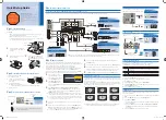
Summary of Contents for TH-42PX50U

Page 1: ...Technical Guide Plasma Training Course TH 37PX50U TH 42PD50U TH 42PX50U TH 42PX500U TH 50PX50U TH 50PX500U GP8DU and GPH8DU Chassis Troubleshooting Panasonic Services Company National Training ...

Page 2: ...d Unauthorized copying and distribution is a violation of law Warning This service information is designed for experienced repair technicians only and is not designed for use by the general public It does not contain warnings or cautions to advise non technical individuals of potential dangers in attempting to service a product Products powered by electricity should be serviced or repaired only by...

Page 3: ...n Operation 12 Power Supply Connections 15 P Board 15 PA Board 16 PB Board 17 TH 42PX500U Block Diagram 18 TH 42PX50U Block Diagram 21 TH 42PD50U Block Diagram 23 Video Input Selection Block Diagram 25 Audio Input Selection Block Diagram 26 ATSC SD and PC Card Input Signal Flow 27 DG Board Block Diagram 28 Signal Process Circuit 30 Main Picture Signal Flow 30 Sub Picture Signal Flow 30 RGB Process...

Page 4: ...Other SOS Detection Circuits 46 SOS Detect P SC and SS Board 46 P Board SOS Detection 47 Voltage Distribution of the PA board and SOS Detection 48 Z Board Sound SOS Detection 50 TH 42 50PX500U Self check Function Reset 51 Diagnostic Procedures 51 How to access the Self check Screen Reset 51 How to exit the Self check Screen 51 Screen Display 51 TH 42PD50U 53 Power LED Flashing timing chart 53 TH 4...

Page 5: ...ocations 62 Troubleshooting 63 No Picture or Partial Picture 63 Scan and Sustain Drive Waveform 66 Scan and Sustain Drive Check points 66 Vertical line problems 71 Picture ok Sound NG 72 No picture no sound 73 No picture sound ok 74 How to determine whether the D board or SC board is defective 75 Additional Troubleshooting Hints 76 SC20 or D20 Connector 77 How to determine whether the D board or S...

Page 6: ...n for new circuits employed in this line of Plasma models Provide drawings with emphasis on signal path to simplify the task of signal tracing and locate the cause of a defect Furnish troubleshooting procedures that contribute to a speedier repair of the product Provide examples of typical problems that may have occurred in similar types of circuits 1 ...

Page 7: ...No Yes Yes Input Terminal Video Input Video 1 S2 RCA Rear S2 RCA Rear S2 RCA Rear Video 2 S2 RCA Rear S2 RCA Rear S2 RCA Rear Video 3 No S2 RCA Front S2 RCA Front Component 1 RCA Rear RCA Rear RCA Rear Component 2 RCA Rear RCA Rear RCA Rear PC Input No Yes x 1 Mini D Sub 15 pin Rear Yes x 1 Mini D Sub 15 pin Rear HDMI Input Yes x 1 Rear Yes x 1 Rear Yes x 1 Rear Card Interface Cable Card Slot No Y...

Page 8: ... an electrical assembly equipped with ES devices place the assembly on a conductive surface such as an aluminum foil to prevent electrostatic charge buildup or exposure on the assembly 6 Use a grounded tip soldering iron to solder or unsolder ES devices 7 Use an anti static solder removal device Some solder removal devices not classified as anti static ESD protected can generate electrical charge ...

Page 9: ...A3598AB DT ATSC Interface TNAG156 DV HDMI Interface TNPA3626 DG Digital Signal Processor TNPA3625AF Z Speaker out Audio AMP TNPA3621AB D Format Converter Plasma AI Processor TZTNP010YFS C1 Data Driver Left TNPA3545 C2 Data Driver Right TNPA3546 SC Scan Drive TNPA3543 SU Scan out Upper TNPA3242 SD Scan out Lower TNPA3243 SS Sustain Drive TNPA3544 K Remote receiver Keyscan TNPA3603 S Power Switch TN...

Page 10: ...ut Audio AMP TNPA3621 D Format Converter Plasma Ai Processor TZTNP010YDS K Remote receiver OPT TNPA3498AB S Power Switch TNPA3499AB C1 Data Driver Up Left TNPA3553AB C2 Data Driver Up Right TNPA3554 C3 Data Driver Down Right TNPA3555 C4 Data Driver Down Left TNPA3556 SC Scan Drive TNPA3557 SU Scan out Up TNPA3189AB SD Scan out Down TNPA3190AB SS Sustain Drive TNPA3558 SS2 Sustain Connector Up TNPA...

Page 11: ... Driver Up Center TNPA3562 C3 Data Driver Up Right TNPA3563 C4 Data Driver Down Right TNPA3564 C5 Data Driver Down Center TNPA3565 C6 Data Driver Down Left TNPA3566 D Format Converter Plasma AI Processor TZTNP010YCS P Power Supply ETXMM564MEK SC Scan Drive TNPA3567 SD Scan out Down TNPA3220AB SS2 Sustain Connector Up TNPA3559 SS Sustain Drive TNPA3568 SS3 Sustain Connector Down TNPA3560 SU Scan ou...

Page 12: ...t and outgoing noise from the unit to the AC outlet The basic operation of the new P board is the same as that of the older Plasma Display Televisions The Standby circuit supplies STB5V and 5V for FAN SOS The main circuit supplies Vsus voltage for sustain and scan operations Vda voltage for data drive C boards 15V for sustain scan and fan operations and 12V for audio power The F_STB14V is used on ...

Page 13: ...de D602 and the transformer T501 are used to develop the STB5V supply The STB5V is applied to pin 5 of the Power control IC MC701 and pin 1 of the Power Control IC MC501 Use hot ground to measure voltage on MC501 See Fig 5 Figure 6 8 ...

Page 14: ...ng the STB5V to be applied to the D and the DG board via pin 10 of the connector P25 See Fig 6 Figure 7 The Microprocessor on the DG board IC4005 receives the regulated STB3 3V from IC4010 Pin 22 of IC4005 outputs 2 5V Tuner SUB ON to the P board via pin 14 of the connectors DG3 D3 and pin 13 of the connector P25 D25 It is then connected to pin 21 F STB ON of the Power Output Control IC MC701 See ...

Page 15: ...ol signal at pin 20 This turns on the photocoupler PC503 to provide a low to pin 2 of the STB Power Control IC MC501 MC501 outputs the relay ON control signal to activate the relay K601 See Fig 8 Figure 9 The rectifier MC604 rectifies the 120VAC from the relay and outputs to the PFC Control MC602 10 ...

Page 16: ...12V power supplies During standby operation both the Vsus and the Vda power supply circuits are off Only the F STB 14V section of the Low Voltage power supply circuit is on Figure 10 The F14V ON command 5V from pin 10 of MC701 turns on Q452 and the F STB 14V is output to the PA board through pins 1 2 and 3 of connector P10 See Fig 10 Note The above description is true for standby mode only the pow...

Page 17: ...C receiver receives the power on command of the remote control and outputs the Q4001 DG board to turn it on When Q4001 is on a low is provided to pin 86 Key scan 3 of the microprocessor IC4005 T IR data to the amplifiers Q4006 and Q4007 of the DG board The data is amplified and output to pin 102 of the MPU IC4005 Figure 12 ...

Page 18: ...located on the DG board It causes Q4008 to stop conducting and output a High to the base of Q9000 on the D board thus turning it on When Q9000 is on the collector goes low This low is applied to the gate of Q9003 turning it on to provide 5V to pins 1 and 2 of IC9008 3 3V Reg The 3 3V out of pin 4 of IC9008 is connected to the VCC pins 3 24 25 28 64 89 and 100 of the microprocessor IC9003 The 3 3V ...

Page 19: ...circuit of the PB board via pin 4 of the connector P30 See Fig 14 The 5V on pin 22 of IC MC303 causes it to operate IC MC303 then turns on the Vsus power supply circuit MC301 and the Vda power supply circuit IC301 and T301 Vsus is output to SC and SS boards Vda is output to the Data Drive Circuit boards via the SC board The low from pin 12 is used to turn on Q453 and Q451 When Q453 is on it output...

Page 20: ...wer Supply Connections P Board Figure 14 The P board houses the main power supply of the unit All voltages originate from this board The connector information is to be used for troubleshooting purposes 15 ...

Page 21: ...Figure 15 The PB board utilizes voltages obtained from the P board to create lower and higher voltages for use in different sections of the unit The connector information can prove useful when troubleshooting 16 ...

Page 22: ...PB Board Figure 16 The PB board contains voltage regulators that power the Audio circuit Z board and the fans The connector information is to be used for troubleshooting purposes 17 ...

Page 23: ...ncorporates the OpenCable interface for use with a CableCard This tuner allows the reception of Digital Cable television without the use of a set top box The DT board contains an Optical Audio Out jack for use with a Dolby Digital decoder and a multi channel amplifier When a digital channel is selected the output from the Digital Audio Out jack is Dolby Digital The same jack outputs PCM Pulse Code...

Page 24: ...ectly connected to the main switch of the H board The H board selects and outputs to the DG board the main video and sub video signals for display on the screen The DG board is responsible for the complete video processing within the unit All analog inputs to the DG board are immediately converted to digital All signal processing in the DG board is performed digitally Signals from a digital TV or ...

Page 25: ... of the SC board into parallel data to drive the panel The SS board is responsible for the generation of the sustain pulses Sustain pulses are used to initialize and control the brightness of the screen The SS2 and SS3 boards are extension connector boards used to connect the SC board to the panel 20 ...

Page 26: ...corporates the OpenCable interface for use with a Cable Card This tuner allows the reception of Digital Cable television without the use of a set top box The DT board contains an Optical Audio Out jack for use with a Dolby Digital decoder and a multi channel amplifier When a digital channel is selected the output from the Digital Audio Out jack is Dolby Digital The same jack outputs PCM Pulse Code...

Page 27: ...etc The board also performs pixel conversion to change the resolution of the picture to the resolution of the screen The output signal of the board passes through an LVDS Low Voltage Differential Signaling transmitter for conversion into serial data The PEAKS firmware of the unit also resides in this board The D board is responsible for displaying the picture on the screen It provides the scan sus...

Page 28: ...ion of basic Digital Cable television without the use of a set top box The DT board contains an Optical Audio Out jack for use with a Dolby Digital decoder and a multi channel amplifier When a digital channel is selected the output from the Digital Audio Out jack is Dolby Digital The same jack outputs PCM Pulse Code Modulation when any other signal source is selected An SD card slot is also includ...

Page 29: ... the resolution of the screen The output signal of the board passes through an LVDS Low Voltage Differential Signaling transmitter for conversion into serial data The PEAKS firmware of the unit also resides in this board The D board is responsible for displaying the picture on the screen It provides the scan sustain and data drive signals The scan pulses are output to the SC board The sustain puls...

Page 30: ...C2605 which selects the audio input signals Video signals from the digital tuner and the HDMI receiver board DV board pass through the DG board and enter IC2602 of the H board via the connector H2 DG2 The selected video signals are output to the DG Board without alteration The output signals can be in any of the three formats Video Y C or Y Pb Pr The PC input signal simply passes through the H boa...

Page 31: ...2605 of the H board via the connector H2 DG2 The selected audio signals are output to the DG Board without alteration The audio output at pin 38 and 40 of the connector H2 DG2 passes through the DG board and enters the DT Board for conversion into PCM Pulse Code Modulation audio Pins 29 and 30 of IC2605 provide the audio for the program out jack IC2608 contains the BBE VIVA technology circuit used...

Page 32: ...nformation is already programmed in the CableCard If a terrestrial antenna is used the unit may be instructed to scan only analog or digital terrestrial broadcast The unit may also be instructed to scan all analog and digital broadcast channels The DT board contains an Optical Audio Out jack for use with a Dolby Digital decoder and a multi channel amplifier When a digital channel is selected the o...

Page 33: ...l incoming video signals The ATSC interface DT board processes the ATSC NTSC and QAM television signals It also processes the Photoviewer JPEG data of the SD and PC cards The composite luminance and chrominance or digital component signal of the DT board are output to the DG board via the connector DT12 DG22 The composite video of the analog TV reception as well as the luminance and chrominance ou...

Page 34: ...The Main and sub video output of the H board are provided to the DG board via the connector H2 DG2 The input signals can be in any of the three formats Video Y C or Y Pb Pr 29 ...

Page 35: ...Chroma demodulator circuit that separates the color signal into Pb and Pr data At the completion of this process the composite or S Video signal is now in the form of a digital 480i component signal If the incoming video is in the 480p and 1080i format the Y Pb and Pr signals are converted to digital only The output of IC4018 is provided to the RGB processor GC4PRO Sub Picture Signal Flow The sub ...

Page 36: ...of the 480P 720P and 1080i formats simply pass through the IP converter The CT1 CR1 AI DSC circuit reduces noise and improves the picture quality On Screen Display data such as channel numbers Digital TV closed caption and picture adjustments are mixed with the video data This circuit performs all picture control operations such as brightness contrast color tint etc The output signal is then appli...

Page 37: ... white balance contrast and color drives are performed inside this IC IC9300 contains the Plasma AI Adaptive brightness Intensifier circuit that analyzes the video program level for the distribution of dark and bright components The Sub field Processor is used to speed up the scanning process and to control the number of sustain periods This increases the brightness and improves the contrast ratio...

Page 38: ...nto four equal quadrants as indicated in the picture on the right Figure 28a Figure 28b Each data drive board contains four sockets for the connection of the panel s ribbon cables Each ribbon cable is mounted in a specific location to drive of the quadrant Furthermore each connector s information is divided into 2 to separately drive two 1 8 of the quadrant See the figure on the right 33 ...

Page 39: ...vers Connector SC20 provides the drive voltages 140V 100V and 18V as well as the trigger signals to switch the FET transistors The D board switches the FETs on and off to create the distinctive scan signal Each trigger signal switches a drive FET creating a portion of the waveform For example applying the CPH signal to the 140V FET creates the peak portion of the waveform see figure 29 34 ...

Page 40: ...SC board Waveform Figure 30 SU And SD Board Shift Registers Figure 31 35 ...

Page 41: ...plied to the SU and SD boards for de multiplexing The signal is input to a series of shift registers inside the PDP scan driver IC The figure above shows an example of the de multiplexing circuit There are six driver ICs on the SU board and six on the SD board 36 ...

Page 42: ...e output to the SS board The erase pulse is output at the beginning of each scan period The pulse is applied to the SS2 and SS3 boards to remove the previous charge from the upper and lower sections of the display panel The sustain pulses are also developed on the D board and are applied after the scan periods 37 ...

Page 43: ...SS Board Schematic Figure 33 SS Board Waveform Figure 34 38 ...

Page 44: ...are applied to FET drivers creating the distinctive sustain pulse The drivers switch the voltages 150V 155V and 175V at selected intervals determined by the D board The basic waveform remains constant but the exact number of sustain pulses is determined by the amount of luminance required see the figure above 39 ...

Page 45: ...D blinks Blinking Timing Suspected Board 1 D P board 4 P PA board Power SOS 5 D P board 5V SOS 6 SC board SC Energy recovery and SC floating voltage 7 SS Board SS Data Energy recovery and data driver 8 SS board SS Energy recovery 9 Incorrect D DG board 10 PA Board No power for tuner 11 PB board Fan Fan SOS 12 H PB Z Board Sound SOS Speaker shorted Table 4 Note LED indicators on the SS and SC board...

Page 46: ...ivated by some fault within the receiver the problem facing the technician is to find out which protection circuit is shutting down the receiver and why Figure 36 SOS Detect DG Board The MPU IC4005 of the DG board is used to detect and store the history of other abnormalities that may be caused by a defect in certain sections of the unit The input pins of the MPU as shown in the figure on the righ...

Page 47: ...A and the PB boards The abnormality may due to an over voltage or a short circuit located on the PA or one of the boards powered by PA board The SOS input at pin 111 is an active high when an abnormality is detected The MPU IC9003 of the D board monitors a variety of SOS inputs All other SOS conditions are monitored by IC4005 located on the D board see fig 37 Upon detection the MPU IC9003 of the D...

Page 48: ... MAIN_3 3V MAIN_5V MAIN_9V and MAIN_2 5V lines If any of these supply voltages becomes excessive the inline zener diode goes into conduction and turn on transistor Q5644 As a result a voltage drop appears at the base of Q5641 causing it to turn on and output a high to pin 111 of the MPU IC4005 to trigger the SOS condition 43 ...

Page 49: ... Figure 40 The transistor Q5642 monitors the MAIN_9V MAIN_2 5V and MAIN_5V lines If any of these supply lines develop a short circuit transistor Q5642 goes into conduction and applies a high to pin 111 of the MPU IC4005 triggering an SOS condition 44 ...

Page 50: ...e 41 The transistor Q5641 monitors the F_STB14V SUB3 3V SUB9V 1 BT30V and SUB5V lines If any of these supply lines develop a short circuit transistor Q5641 goes into conduction and applies a high to pin 111 of the MPU IC4005 triggering an SOS condition 45 ...

Page 51: ...ector of the board causing the blinks of the power LED may be disconnected to see if the unit remains on after power up If it does this usually indicates that the problem is located in the disconnected board If the power LED continues to generate the same amount of blinks more troubleshooting is required Note The unit will become totally inoperative if the power supply to the D and DG boards is di...

Page 52: ... voltmeter the power supply connector of the suspected board causing the blinks of the power LED may be disconnected to see if the unit remains on after power up If it does this usually indicates that the problem is located in the disconnected board If the power LED continues to generate the same amount of blinks more troubleshooting is required Note The unit will become totally inoperative if the...

Page 53: ...This SOS condition is created when there is an abnormality of any of the voltages shown in the diagram Instead of using a peak hold voltmeter the power supply connector of the board causing the blinks of the power LED may be disconnected to see if the unit remains on after power up If it does this usually indicates that the problem is located in the disconnected board If the power LED continues to...

Page 54: ...The purpose of this pictorial of the component side of the PA board is to alert the technicians of the labeling and actual location of some the diodes mounted on the PA board Figure 45 49 ...

Page 55: ...ing the Z board The main 9V source of the PA board is also used on the Z board It passes through the H board and then enters the Z board On the Z board the transistor Q2323 monitors the 10 and 9 volts sources for a short If a short is detected a high output is provided to the base of Q2324 resulting in a low output to pin 15 of IC4005 Twelve blinks are generated when an abnormality is detected 50 ...

Page 56: ...on the remote control Hold them down for at least three seconds The unit automatically tunes to channel 3 The word SELF CHECK appears at the center of the screen for a few seconds and then a graphic OSD that resembles the one in the figure below appears How to exit the Self check Screen To exit the Self check mode press the power button in front of the unit for approximately three seconds The unit...

Page 57: ...oard DT2 IC8240 HDMSL PEAKS_Lite DT Board H13UV2 SND IC2608 BBE Viva H Board AVSWV IC2602 Video SW H Board AVSWA IC2605 Audio SW H Board ADV IC4018 10 Bits A D DG Board GC3FS IC4019 GC3FS DG Board GC4P IC4026 GC4PRO DG Board HDMI IC5003 HDMI I F Receiver DV Board MEM IC4008 EEPROM DG Board RTC IC9007 Ex I O D Board Table 5 52 ...

Page 58: ...he number of flashes emitted by the power LED located in front of the unit Number of Power LED blinks Blinking Timing Suspected Board 1 D P board 4 P PA board Power SOS 5 D P board 5V SOS 6 SC board SC E recovery and nergy SC floating voltage 7 SS Board SS Data Energy recovery and data driver 8 SS board SS Energy recovery 9 Incorrect D DG board 10 PA Board No power for tuner 11 PB board Fan Fan SO...

Page 59: ...ton on the remote control Hold them down for at least three seconds The unit self tunes to channel 3 The word SELF CHECK appears at the center of the screen for a few seconds and then a graphic OSD that resembles the one in the figure below appears How to exit the Self check Screen To exit the Self check mode press the power button in front of the unit for approximately three seconds The unit powe...

Page 60: ...sor DT Board DT2 IC8240 HDMSL PEAKS_Lite DT Board SND IC2608 BBE Viva H Board AVSWV IC2602 Video SW H Board AVSWA IC2605 Audio SW H Board H34DG IC4026 GC4PRO DG Board GC4P IC4018 10Bits A D DG Board HDMI IC5003 HDMI I F Receiver DV Board MEM IC4008 EEPROM DG Board RTC IC9007 Ex I O D Board Table 7 55 ...

Page 61: ...s in reverse direction Use the VOLUME UP and VOLUME DOWN buttons of the remote control to change the value of the Sub Items Cancellation To exit the serviceman mode switch off the power by pressing the POWER button of the main unit Figure 49 Contents of adjustment mode 1 The value is shown as a hexadecimal number 2 The preset value differs depending on models 3 After entering the adjustment mode w...

Page 62: ...d the VOLUME UP button of the remote control for 2 seconds FDC Status System FAT Status Press EXIT to return OK for more information Polarity Non Inverted SNR 18 dB Packet Count 3331 CH Map Available VCM OK MMS OK DCM OK CDS OK Hidden 1 Undef 1 Mod Frq Video Channel Status PCR Status Locked PCR pid 0x0021 Video pid 0x0021 Audio pid 0x0022 CC708 Activated Type Digital Elapsed time 4 days 3 hr 6 min...

Page 63: ...BOARD Vsus 2V VR351 P BOARD Ve TPVE SS BOARD Ve 1V VR6145 SS BOARD Vset TPVSET SC BOARD 240 V 7V Verify Only Vad TPVAD SC BOARD 105 1V VR6477 SC BOARD Vda TPVDA SS Board 70V 1V Verify only VSCN TPVSCN SC BOARD Vad 130V 4V Verify only Refer to the panel label for the exact value Table 9 TH 50PX500 Name Test point Voltage Volume Vsus TPVSUS SS BOARD Vsus 2V VR351 P BOARD Ve TPVE SS BOARD Ve 1V VR625...

Page 64: ...djustments Adjust the indicated test point for the specified waveform Use test point TPSS1 of the SS board as the trigger source Test point Volume Level Remark 10 10 5µ Sec TH 42PX500U T1 TPSC1 SC 20 15µ Sec TH 50PX500U VR6557 SC 210 10µ Sec TH 42PX500U T2 TPSC1 SC VR6602 SC 155 10µ Sec TH 50PX500U Table 11 Drive Waveform Figure 52 59 ...

Page 65: ...st Point Voltage Volume Remarks P Board Vsus TPVSUS SS Vsus 2V VR351 P SC Board Vad TPVAD SC 105V 1V VR6477 SC SS Board Ve TPVE SS Ve 1V VR6145 SS Refer to the Panel label for the exact value Table 12 TH 50 PX500U P C B Name Test Point Voltage Volume Remarks P Board Vsus TPVSUS SS Vsus 2V VR351 P SC Board Vad TPVAD SC 90V 1V VR6801 SC SS Board Ve TPVE SS Ve 1V VR6250 SS Refer to the Panel label fo...

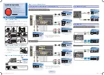
Page 66: ...Adjustment Volume Locations Figure 53 61 ...

Page 67: ...Test Point Locations Figure 54 62 ...

Page 68: ... Board LED illuminated or is the waveform at TPSS1 ok See Ref 2 on page 66 No Yes The SC Board is probably defective SS Board is probably defective The D Board is probably defective Is there 70V VDA at pins 1 and 2 of the connector SS12 No Check the P board Yes Is the picture black or monochromatic noisy Is the picture noisy or mono chromatic No Go to step 3 Go to step 2 Go to step 1 Check the DG ...

Page 69: ...n page 66 Check the D board Check the SC board No No Yes Check the DG or D board Yes No Check the D board Yes No Check the DG board Is the LVDS signal output from the DG Board to the D Board OK Go to Check Point on page 66 Yes Check the P board No Is the Vda voltage at TP_VDA of the SS board OK Is there a dark picture Yes Go to step 1 Go to Step 4 64 ...

Page 70: ...board No Is the SUSTAIN CONTROL PULSE from the D Board to the SS Board OK Go to Check Point on page 66 Yes Check the SS board No Go to Step 5 Check the SU or SC board Yes No No lower half Check the SD or SC board Is the picture problem in the upper half of the screen Is the picture problem in the upper or lower half of the screen Yes upper or lower half Step 4 65 ...

Page 71: ...Scan and Sustain Drive Waveform Figure 55 Scan and Sustain Drive Check points Figure 56 66 ...

Page 72: ...icture problem Right half or left half of the screen Left half of the screen No right half D Board or C1 C4 board Yes left half D Board or C2 C3 board Upper right of the screen Vertical line No picture Is there no picture or a wide vertical line at the upper right of the screen D Board or C1 board PDP Panel See the section entitled Vertical line problem HD model 42 37 inch Step 5 67 ...

Page 73: ...he screen Vertical line PDP Panel No picture D Board or C2 board Is there no picture or a wide vertical line at the left half of the screen Go to step 6 Lower right of the screen Vertical line No picture D Board or C4 board Is there no picture or a wide vertical line at the lower right of the screen PDP Panel Lower left of the screen Vertical line No picture D Board or C3 board Is there no picture...

Page 74: ...a wide vertical line at the upper middle of the screen Where is the picture problem One third of the left middle or right of the screen Left No right or middle D Board or C2 C5 board No middle Yes D Board or C1 C6 board Right Yes D Board or C3 C4 board Upper right of the screen Vertical line No picture Is there no picture or a wide vertical line at the upper right of the screen D Board or C1 board...

Page 75: ...re D Board or C5 board Is there no picture or a wide vertical line at the lower middle of the screen Lower right of the screen Vertical line No picture Check the D Board or C6 board Is there no picture or a wide vertical line at the lower right of the screen PDP Panel Is there no picture or a wide vertical line at the lower left of the screen 70 ...

Page 76: ...ts the C board to the panel To resolve this problem the panel has to be replaced A number of blocks do not light up The likelihood of all four driver ICs of the panel being defective is very small Such a defect usually indicates that the C board may be defective or the D board may not be providing the drive data for the C board To resolve this problem replace the C board first If the problem persi...

Page 77: ...s Check the DT board Check the H board No Is there sound from the AV terminal No sound from digital TV reception Yes Yes Check the TA board Check the H board No Is there sound from the AV terminal No sound from analog TV reception No Check the H board No Is there sound from the program out jacks 72 ...

Page 78: ... sound from digital TV reception Input Source check Check the H board No picture and sound from the AV terminal Yes Check the TA board Check the H board No Is the picture and sound of the AV terminal ok No picture and no sound from analog TV reception 73 ...

Page 79: ...d No picture from digital TV reception Check the H board No picture from the AV terminal No picture from analog TV reception Yes Check the H board No Is there picture from one of the AV inputs Input Source check Yes Check the TA board Check the H and DG board No Is there a picture from the AV terminal 74 ...

Page 80: ...board is defective Figure 58 Note All SCAN CONTROL PULSES are located at pins 2 3 4 6 7 8 9 13 17 18 19 and 20 of connector SC20 D20 A missing waveform at one of the pins with the exception of pins 8 9 and 13 will cause the power LED to blink 75 ...

Page 81: ...ss period of the Scan Drive Signal at pin 8 of connector SC20 D20 has dropped The problem is the D board Figure 59 Symptom 2 Picture Noise Part of the previous picture is visible on the screen Cause The VSET Initialization pulse of the Scan Drive signal at pin 9 of connector SC20 D20 has dropped The problem is the D board Figure 59a 76 ...

Page 82: ...pin 13 of connector SC20 D20 The problem is the D board Figure 60 The approach to find the defective board is to check the pins of the connector listed in the table below Check point SC20 or D20 Connector Pin 8 Pin 9 Pin 13 Defect Board OK OK OK SC Board NG NG OK D Board OK NG OK D Board OK OK NG D Board NG NG NG D Board Table 14 77 ...

Page 83: ... is defective Figure 61 Note All SUSTAIN CONTROL PULSES are located at pins 3 4 5 6 7 and 8 of one of the C see the table above and SS44 connectors A missing waveform at one of the pins with the exception of pin 4 will cause the power LED to blink 78 ...

Page 84: ...e Ve of the initializing and address period of Sustain Drive Signal is missing The problem is the D board Figure 62 The approach to find the defective board is to check pin 4 of the connectors listed in the table below Check Point Model Connector NO Pin NO 37 HD C32 42 SD C23 42 HD C32 50 HD SS44 4 Defective Board OK SS Board NG D Board Table 15 79 ...

Page 85: ...e memory cards FDC STATUS Forward Data Channel Status POD Point Of Deployment PCR Program Clock Reference PID Packet Identification Data HDMI High Definition Multimedia Interface Interface that supports every uncompressed digital format as well as all existing multi channel audio format on a single cable JPEG Joint Photographic Experts Group A system used for compressing decoding color still pictu...

Reviews: