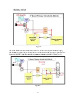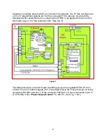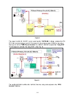
Instead of a standby power switch, as it shows in the diagram, the TV has a jumper wire
on the “S” board that connects pin 8 of the connector P12 to ground. As a result the
transistors Q553 and Q554 turn on, allowing the STB5V to be applied to the D and the
DG-board via pin 10 of the connector P25. (See Fig. 6).
Figure 7
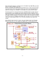
The Microprocessor on the DG board (IC4005) receives the regulated STB3.3V from
IC4010. Pin 22 of IC4005 outputs 2.5V (Tuner SUB ON) to the P board via pin 14 of the
connectors DG3/D3 and pin 13 of the connector P25/D25. It is then connected to pin 21
(F. STB ON) of the
“Power Output Control”
IC
,
MC701. (See Fig. 7 & 8.)
9
Summary of Contents for TH37PX50U - 37" HD PLASMA TV
Page 40: ...SC board Waveform Figure 30 SU And SD Board Shift Registers Figure 31 35 ...
Page 43: ...SS Board Schematic Figure 33 SS Board Waveform Figure 34 38 ...
Page 66: ...Adjustment Volume Locations Figure 53 61 ...
Page 67: ...Test Point Locations Figure 54 62 ...
Page 71: ...Scan and Sustain Drive Waveform Figure 55 Scan and Sustain Drive Check points Figure 56 66 ...


