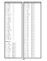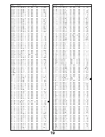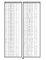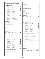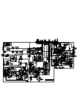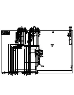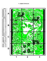
SCHEMATIC DIAGRAMS FOR MODELS
TX-28XD90P /A /B
TX-25XD90P /A /B
(EURO - 5 CHASSIS)
NOTE
1. RESISTOR
All resistors are carbon ¼W resistor, unless marked otherwise.
Unit of resistance is OHM (
Ω
) (k=1,000, M=1,000,000)
2. CAPACITORS
All capacitors are ceramic 50V unless marked otherwise.
Unit of capacitance is
µ
F unless otherwise stated.
3. COIL
Unit of inductance is
µ
H, unless otherwise stated.
4. TEST POINT
Test Point Position
5. EARTH SYMBOL
Chassis Earth (Cold)
Line Earth (Hot)
6. VOLTAGE
MEASUREMENT
Voltage is measured by a d.c. voltmeter.
Measurement conditions are as follows:
Power source
a.c. 220V-240V, 50Hz
Receiving Signal
Colour Bar signal (RF)
All customer controls
Maximum position
7.
Indicates the Video signal path
Indicates the Audio signal path
These schematic diagrams are the latest at time of printing and are subject to change without notice.
REMARKS
a. Do not touch the hot part, or the hot and cold parts at the same time, as you are liable to a shock hazard.
b. Do not short circuit the hot and cold circuits as electrical components may be damaged.
c.
Do not connect an instrument, such as an oscilloscope, to the hot and cold circuits simultaneously as this may cause
fuse failure. Connect the earth of the instruments to the earth connection of the circuit being measured.
d. Make sure to disconnect the power plug before removing the chassis.
NOTE
1. The Power Supply Circuit contains a circuit area, which uses a separate power supply to isolate the earth connection.
The circuit is defined by HOT and COLD indications in the schematic diagram. All circuits, except the Power Circuit, are
COLD.
IMPORTANT SAFETY NOTICE
Components identified by
mark have special characteristics
important for safety. When replacing any of these components, use
only manufacturer's specified parts.
28
Summary of Contents for TX-25XD90P
Page 13: ...32 5 6833 7 21 2 5 0 ...
Page 29: ...NOTES 27 ...
Page 31: ......
Page 32: ......
Page 33: ......
Page 34: ......
Page 35: ......
Page 36: ......
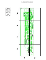
Page 43: ...M BOARD TNP8EM015 TRAN S Q1011 A1 Q1012 A2 DIODE S D1011 A1 I C S IC1011 A1 1 2 A B C D ...

