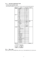
5.2.
Service tool mode
5.2.1.
How to access
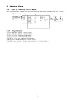
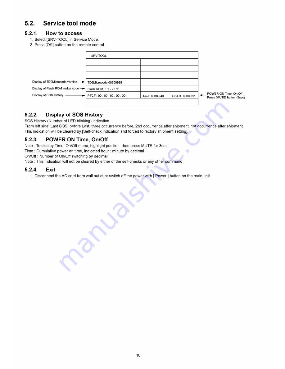
1. Select [SRV-TOOL] in Service Mode.
2. Press [OK] button on the remote control.
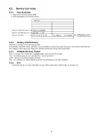
Display of TD2Microcode version —
Display of Flash ROM maker code -
Display of SOS History ---------------
SRV-TOOL
TD2Microcode:00500985
Flash ROM : 1 - 227E
PTCT : 00 . 00 . 00 . 00 . 00
Time 00000:40
On/Off 0000022
. POWER ON Time, On/Off
Press [MUTE] button (3sec)
5.2.2.
Display of SOS History
SOS History (Num ber of LED blinking) indication.
From left side; Last SOS, before Last, three occurrence before, 2nd occurrence after shipment, 1st occurrence after shipment.
This indication will be cleared by [Self-check indication and forced to factory shipment setting].
5.2.3.
POWER ON Time, On/Off
Note : To display Time, O n/Off menu, highlight position, then press MUTE for 3sec.
Time : Cumulative power on time, indicated hour : minute by decimal
O n/Off : Number of O n/Off switching by decimal
Note : This indication will not be cleared by either of the self-checks or any other command.
5.2.4.
Exit
1. Disconnect the AC cord from wall outlet or switch off the power with [ Power ] button on the main unit.
10
Summary of Contents for TX-PR46G10
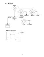
Page 15: ...6 4 No Picture No Picture Check NG 15 ...
Page 27: ...8 1 4 Adjustment Volume Location 8 1 5 Test Point Location 27 ...
Page 32: ...32 ...
Page 33: ...9 Block Diagram 9 1 Main Block Diagram 33 ...
Page 34: ...9 2 Block 1 4 Diagram JK8302 SPEAKER L SPEAKER R SD CARD SLOT 34 ...
Page 35: ... о 0 9 3 Block 2 4 Diagram FOR FACTORY USE FOR FACTORY USE 35 ...
Page 38: ...38 ...
Page 40: ...4 10 3 Wiring 2 40 ...
Page 41: ...10 4 Wiring 3 41 ...
Page 42: ...42 ...
Page 45: ...11 2 P Board 1 2 Schematic Diagram A B C D E F i 2 3 4 5 6 7 44 ...
Page 46: ...11 3 P Board 2 2 Schematic Diagram 45 ...
Page 48: ......
Page 49: ...11 5 A Board 1 20 Schematic Diagram A A B O A R D 1 20 lie REF No 0900 0999 JTAG B D 47 ...
Page 50: ...11 6 A Board 2 20 Schematic Diagram 10 11 12 13 14 15 16 17 18 48 ...
Page 51: ...11 7 A Board 3 20 Schematic Diagram NOT USE 19 20 21 22 23 24 25 26 27 49 ...
Page 52: ...0 11 8 A Board 4 20 Schematic Diagram NOT USE 2 8 1 29 1 30 1 31 1 32 1 33 1 34 1 35 1 36 50 ...
Page 53: ...11 9 A Board 5 20 Schematic Diagram SUB3 3V SUB SD 3 3V T r 37 38 39 40 ...
Page 54: ...j 41 42 43 44 45 51 ...
Page 57: ...11 12 A Board 8 20 Schematic Diagram A A B O A R D 8 20 A D V V 64 65 66 67 68 69 70 71 72 54 ...
Page 58: ...11 13 A Board 9 20 Schematic Diagram A A B O A R D 9 20 A D V V REF No 4500 4799 73 74 75 76 ...
Page 59: ...55 ...
Page 60: ...11 14 A Board 10 20 Schematic Diagram 56 ...
Page 62: ...95 96 97 98 99 57 ...
Page 64: ...ТО 13 20 104 105 106 107 108 58 ...
Page 66: ...11 18 A Board 14 20 Schematic Diagram 118 119 120 121 122 123 124 125 126 60 ...
Page 69: ...11 21 A Board 17 20 Schematic Diagram 145 1 146 1 147 1 148 1 149 1 150 1 151 1 152 1 153 63 ...
Page 72: ...168 169 170 171 ...
Page 78: ...11 29 C3 Board 2 2 Schematic Diagram A С З B O A R D T N P A 4 7 6 6 2 2 10 11 12 13 ...
Page 79: ...DRIVER 15 16 17 18 ...
Page 81: ...11 31 SC Board 2 4 Schematic Diagram 10 11 12 13 14 15 16 17 18 73 ...
Page 82: ...11 32 SC Board 3 4 Schematic Diagram 19 2 0 21 22 23 24 2 5 26 27 74 ...
Page 83: ...11 33 SC Board 4 4 Schematic Diagram 28 1 29 1 30 1 31 1 32 1 33 1 34 1 35 1 36 75 ...
Page 89: ...P BOARD COMPONENT SIDE ETX2MM747MFK 6 5 4 3 2 1 A I B I C I D I E I F I G I H I I 80 ...
Page 93: ...F I G I H ...
Page 95: ...A BOARD COMPONENT SIDE A PR46G10 ...
Page 100: ...12 8 SC Board SC BOARD FOIL SIDE TNPA4782AC A В С D ...
Page 101: ......
Page 104: ...SC BOARD COMPONENT SIDE TNPA4782AC 6 5 4 3 2 1 A I B I C I D I E I F I G I H I I 90 ...
Page 108: ...13 1 2 Packing 1 94 ...
Page 109: ...95 ...

