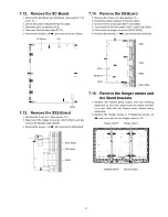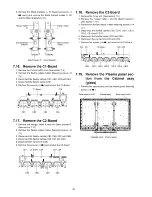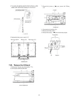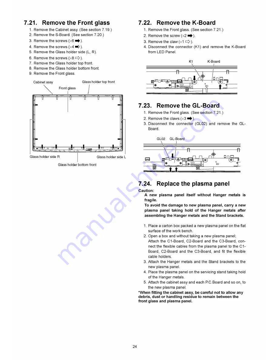
7.21. Remove the Front glass
1. Remove
2. Remove
3. Remove
Remove
Remove
Remove
Remove
Remove
Remove
the Cabinet assy. (See section 7.19.
the S-Board. (See section 7.20.)
the screws (x6 ^ ) .
the screws (x4 Н » .
the Glass holder side (L, R).
the screws (x8 O ) -
the Glass holder top front.
the Glass holder bottom front.
the Front glass.
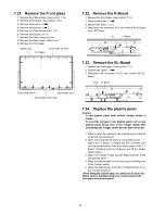
7.22. Remove the K-Board
1. Remove the Front glass. (See section 7.21.)
2. Remove the screw (x2 ^ ) .
3. Remove the claw (x1 cz|>)-
4. Disconnect the connector (K1) and remove the K-Board
from LED Panel.
7.23. Remove the GL-Board
1. Remove the Front glass. (See section 7.21.)
2. Remove the claws (x3 ^ ) .
3. Disconnect the connector (GL02) and remove the GL-
Board.
7.24. Replace the plasma panel
Caution:
A new plasma panel itself without Hanger metals is
fragile.
To avoid the dam age to new plasma panel, carry a new
plasm a panel taking hold o f the Hanger metals after
assembling the Hanger metals and the Stand brackets.
1. Place a carton box packed a new plasma panel on the flat
surface of the w ork bench.
2. Open a box and without taking a new plasma panel;
Attach the C1-Board, C2-Board and the C3-Board, con
nect the flexible cables from the plasma panel to the C1-
Board, C2-Board and the C3-Board, and fit the flexible
cable holders.
3. Attach the H anger metals and the Stand brackets to the
new plasma panel.
4. Place the plasma panel on the servicing stand taking hold
of the Hanger metals.
5. Attach the cabinet assy and each P.C.Board and so on, to
the new plasma panel.
*W hen fitting the cabinet assy, be careful not to allow any
debris, dust or handling residue to remain between the
front glass and plasma panel.
24
Summary of Contents for TX-PR46G10
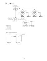
Page 15: ...6 4 No Picture No Picture Check NG 15 ...
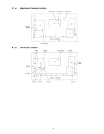
Page 27: ...8 1 4 Adjustment Volume Location 8 1 5 Test Point Location 27 ...
Page 32: ...32 ...
Page 33: ...9 Block Diagram 9 1 Main Block Diagram 33 ...
Page 34: ...9 2 Block 1 4 Diagram JK8302 SPEAKER L SPEAKER R SD CARD SLOT 34 ...
Page 35: ... о 0 9 3 Block 2 4 Diagram FOR FACTORY USE FOR FACTORY USE 35 ...
Page 38: ...38 ...
Page 40: ...4 10 3 Wiring 2 40 ...
Page 41: ...10 4 Wiring 3 41 ...
Page 42: ...42 ...
Page 45: ...11 2 P Board 1 2 Schematic Diagram A B C D E F i 2 3 4 5 6 7 44 ...
Page 46: ...11 3 P Board 2 2 Schematic Diagram 45 ...
Page 48: ......
Page 49: ...11 5 A Board 1 20 Schematic Diagram A A B O A R D 1 20 lie REF No 0900 0999 JTAG B D 47 ...
Page 50: ...11 6 A Board 2 20 Schematic Diagram 10 11 12 13 14 15 16 17 18 48 ...
Page 51: ...11 7 A Board 3 20 Schematic Diagram NOT USE 19 20 21 22 23 24 25 26 27 49 ...
Page 52: ...0 11 8 A Board 4 20 Schematic Diagram NOT USE 2 8 1 29 1 30 1 31 1 32 1 33 1 34 1 35 1 36 50 ...
Page 53: ...11 9 A Board 5 20 Schematic Diagram SUB3 3V SUB SD 3 3V T r 37 38 39 40 ...
Page 54: ...j 41 42 43 44 45 51 ...
Page 57: ...11 12 A Board 8 20 Schematic Diagram A A B O A R D 8 20 A D V V 64 65 66 67 68 69 70 71 72 54 ...
Page 58: ...11 13 A Board 9 20 Schematic Diagram A A B O A R D 9 20 A D V V REF No 4500 4799 73 74 75 76 ...
Page 59: ...55 ...
Page 60: ...11 14 A Board 10 20 Schematic Diagram 56 ...
Page 62: ...95 96 97 98 99 57 ...
Page 64: ...ТО 13 20 104 105 106 107 108 58 ...
Page 66: ...11 18 A Board 14 20 Schematic Diagram 118 119 120 121 122 123 124 125 126 60 ...
Page 69: ...11 21 A Board 17 20 Schematic Diagram 145 1 146 1 147 1 148 1 149 1 150 1 151 1 152 1 153 63 ...
Page 72: ...168 169 170 171 ...
Page 78: ...11 29 C3 Board 2 2 Schematic Diagram A С З B O A R D T N P A 4 7 6 6 2 2 10 11 12 13 ...
Page 79: ...DRIVER 15 16 17 18 ...
Page 81: ...11 31 SC Board 2 4 Schematic Diagram 10 11 12 13 14 15 16 17 18 73 ...
Page 82: ...11 32 SC Board 3 4 Schematic Diagram 19 2 0 21 22 23 24 2 5 26 27 74 ...
Page 83: ...11 33 SC Board 4 4 Schematic Diagram 28 1 29 1 30 1 31 1 32 1 33 1 34 1 35 1 36 75 ...
Page 89: ...P BOARD COMPONENT SIDE ETX2MM747MFK 6 5 4 3 2 1 A I B I C I D I E I F I G I H I I 80 ...
Page 93: ...F I G I H ...
Page 95: ...A BOARD COMPONENT SIDE A PR46G10 ...
Page 100: ...12 8 SC Board SC BOARD FOIL SIDE TNPA4782AC A В С D ...
Page 101: ......
Page 104: ...SC BOARD COMPONENT SIDE TNPA4782AC 6 5 4 3 2 1 A I B I C I D I E I F I G I H I I 90 ...
Page 108: ...13 1 2 Packing 1 94 ...
Page 109: ...95 ...

