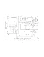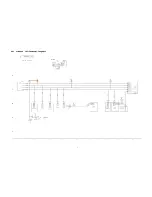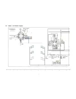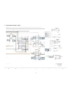
Remarks:
1. The Power Circuit contains a circuit area which uses a separate power supply to isolate the
earth connection.
The circuit is defined by HOT and COLD indications in the schematic diagram. Take the
follwing precautions.
All circuits, except the Power Circuit, are cold.
Precautions
a. Do not touch the hot part or the hot and cold parts at the same time or you may
be shocked.
b. Do not short- circuit the hot and cold circuits or a fuse may blow and parts may
break.
c. Do not connect an instrument, such as an oscilloscope, to the hot and cold
circuits simultaneously or a fuse may blow.
Connect the earth of instruments to the earth connection of the circuit being
measured.
d. Make sure to disconnect the power plug before removing the chassis.
3
Summary of Contents for TX-PR46G10
Page 15: ...6 4 No Picture No Picture Check NG 15 ...
Page 27: ...8 1 4 Adjustment Volume Location 8 1 5 Test Point Location 27 ...
Page 32: ...32 ...
Page 33: ...9 Block Diagram 9 1 Main Block Diagram 33 ...
Page 34: ...9 2 Block 1 4 Diagram JK8302 SPEAKER L SPEAKER R SD CARD SLOT 34 ...
Page 35: ... о 0 9 3 Block 2 4 Diagram FOR FACTORY USE FOR FACTORY USE 35 ...
Page 38: ...38 ...
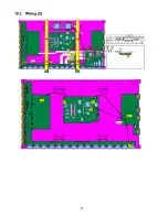
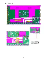
Page 40: ...4 10 3 Wiring 2 40 ...
Page 41: ...10 4 Wiring 3 41 ...
Page 42: ...42 ...
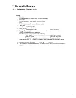
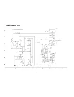
Page 45: ...11 2 P Board 1 2 Schematic Diagram A B C D E F i 2 3 4 5 6 7 44 ...
Page 46: ...11 3 P Board 2 2 Schematic Diagram 45 ...
Page 48: ......
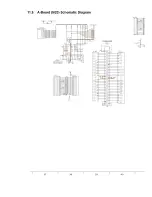
Page 49: ...11 5 A Board 1 20 Schematic Diagram A A B O A R D 1 20 lie REF No 0900 0999 JTAG B D 47 ...
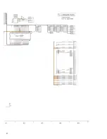
Page 50: ...11 6 A Board 2 20 Schematic Diagram 10 11 12 13 14 15 16 17 18 48 ...
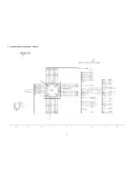
Page 51: ...11 7 A Board 3 20 Schematic Diagram NOT USE 19 20 21 22 23 24 25 26 27 49 ...
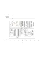
Page 52: ...0 11 8 A Board 4 20 Schematic Diagram NOT USE 2 8 1 29 1 30 1 31 1 32 1 33 1 34 1 35 1 36 50 ...
Page 53: ...11 9 A Board 5 20 Schematic Diagram SUB3 3V SUB SD 3 3V T r 37 38 39 40 ...
Page 54: ...j 41 42 43 44 45 51 ...
Page 57: ...11 12 A Board 8 20 Schematic Diagram A A B O A R D 8 20 A D V V 64 65 66 67 68 69 70 71 72 54 ...
Page 58: ...11 13 A Board 9 20 Schematic Diagram A A B O A R D 9 20 A D V V REF No 4500 4799 73 74 75 76 ...
Page 59: ...55 ...
Page 60: ...11 14 A Board 10 20 Schematic Diagram 56 ...
Page 62: ...95 96 97 98 99 57 ...
Page 64: ...ТО 13 20 104 105 106 107 108 58 ...
Page 66: ...11 18 A Board 14 20 Schematic Diagram 118 119 120 121 122 123 124 125 126 60 ...
Page 69: ...11 21 A Board 17 20 Schematic Diagram 145 1 146 1 147 1 148 1 149 1 150 1 151 1 152 1 153 63 ...
Page 72: ...168 169 170 171 ...
Page 78: ...11 29 C3 Board 2 2 Schematic Diagram A С З B O A R D T N P A 4 7 6 6 2 2 10 11 12 13 ...
Page 79: ...DRIVER 15 16 17 18 ...
Page 81: ...11 31 SC Board 2 4 Schematic Diagram 10 11 12 13 14 15 16 17 18 73 ...
Page 82: ...11 32 SC Board 3 4 Schematic Diagram 19 2 0 21 22 23 24 2 5 26 27 74 ...
Page 83: ...11 33 SC Board 4 4 Schematic Diagram 28 1 29 1 30 1 31 1 32 1 33 1 34 1 35 1 36 75 ...
Page 89: ...P BOARD COMPONENT SIDE ETX2MM747MFK 6 5 4 3 2 1 A I B I C I D I E I F I G I H I I 80 ...
Page 93: ...F I G I H ...
Page 95: ...A BOARD COMPONENT SIDE A PR46G10 ...
Page 100: ...12 8 SC Board SC BOARD FOIL SIDE TNPA4782AC A В С D ...
Page 101: ......
Page 104: ...SC BOARD COMPONENT SIDE TNPA4782AC 6 5 4 3 2 1 A I B I C I D I E I F I G I H I I 90 ...
Page 108: ...13 1 2 Packing 1 94 ...
Page 109: ...95 ...

